

Page 1
DESCRIPTION
The TDA1908 is a monolithic integrated circuit in
12 lead quad in-line plastic package intended for
lowfrequencypowerapplications.Themountingis
compatiblewith the old types TBA800, TBA810S,
TCA830Sand TCA940N. Its main featuresare:
– flexibility in use with a max output curent of 3A
and an operating supply voltage range of 4V to
30V;
– protectionagainst chip overtemperature;
– soft limiting in saturationconditions;
– low ”switch-on”noise;
– low numberof externalcomponents;
– high supplyvoltagerejection;
– very low noise.
ABSOLUTE MAXIMUM RATINGS
TDA1908
8W AUDIOAMPLIFIER
Findip
ORDERING NUMBER : TDA1908
Symbol Parameter Value Unit
V
s
I
o
I
o
P
tot
T
stg,Tj
Supply voltage 30 V
Output peak current(non repetitive) 3.5 A
Output peak current(repetitive) 3 A
Power dissipation: at T
Storage and junctiontemperature -40 to 150
=80°C
amb
at T
=90°C5W
amb
1W
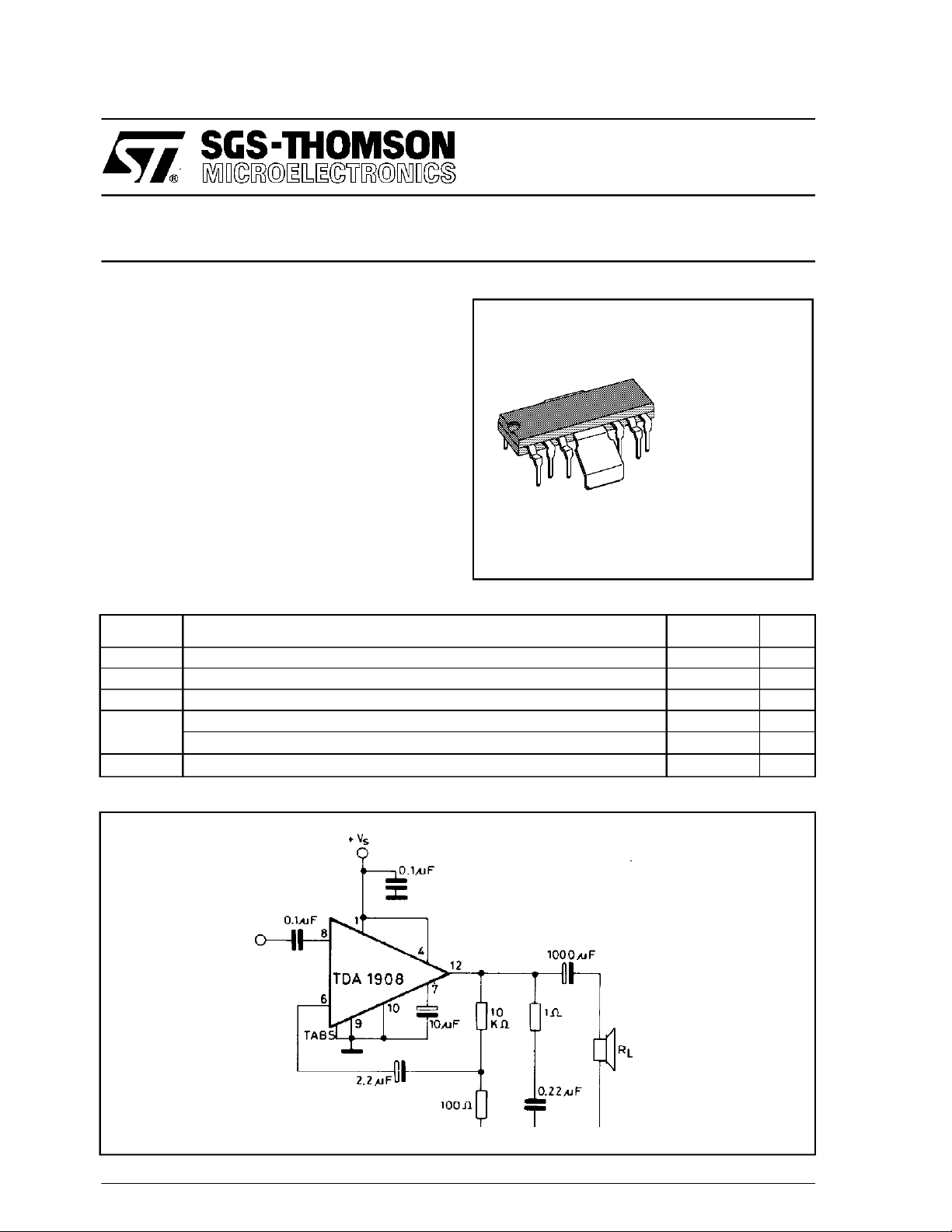
APPLICATION CIRCUIT
°C
March 1993
1/12
Page 2
TDA1908
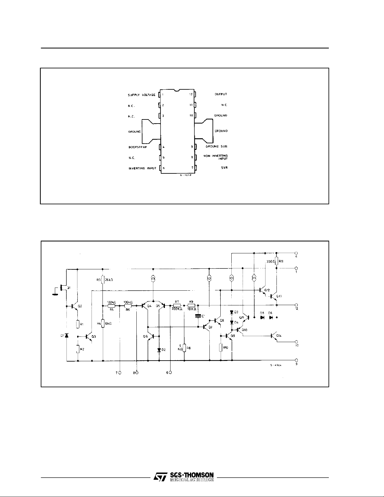
PIN CONNECTION(top view)
SCHEMATIC DIAGRAM
2/12
Page 3
TDA1908
TEST CIRCUIT
* See fig. 12
THERMALDATA
Symbol Parameter Value Unit
R
th j-tab
R
th j-amb
(°) Obtained withtabs solteredto printed circuit board withmin copper area.
ELECTRICAL CHARACTERISTICS (Refertothetest circuit, T
Thermal resistancejunction-tab max 12
Thermal resistancejunction-ambient max (°)70
=25°C, Rth(heatsink)=8 °C/W, unless
amb
°C/W
°C/W
otherwisespecified)
Symbol Parameter Testconditions Min. Typ. Max. Unit
Supply voltage 4 30 V
V
s
2.5
10.2
16.8
V
Quiescent output voltage Vs=4V
V
o
I
Quiescent drain current Vs=4V
d
Output stage saturation voltage
CEsat
(each output transistor)
Output power
P
o
V
= 18V
s
V
= 30V
s
V
= 18V
s
V
= 30V
s
IC=1A
= 2.5A
I
C
d = 10% f = 1KHz
V
=9V RL=4Ω
s
V
= 14V RL=4Ω
s
V
= 18V RL=4Ω
s
V
= 22V RL=8Ω
s
V
= 24V RL=16Ω
s
1.6
8.2
14.4
7
6.5
4.5
2.1
9.2
15.5
15
17.5
21 35
0.5
1.3
2.5
5.5
9
8
5.3
V
mA
V
W
3/12
Page 4

TDA1908
ELECTRICAL CHARACTERISTICS (continued)
Symbol Parameter Testconditions Min. Typ. Max. Unit
d Harmonic distorsion
Input sensivity Vs=9V
V
i
V
Input saturation voltage (rms) Vs=9V
i
R
Input resistence (pin 8) f = 1 KHz 60 100
i
I
Drain current f = 1 KHz
s
Efficiency
η
BW Small signal bandwitdth (-3 dB) V
f = 1KHz
V
=9V RL=4Ω
s
P
= 50 mW to 1.5 W
V
V
V
V
V
V
V
V
V
V
V
V
V
V
o
= 18V RL=4Ω
s
= 24V RL=16Ω
s
= 14V
s
= 18V
s
= 22V
s
= 24V
s
= 14V
s
= 18V
s
= 24V
s
= 14V
s
= 18V
s
= 22V
s
= 24V
s
= 18V f = 1 KHz
s
= 18V
s
=50mWto4W
P
o
P
=50mWto3W
o
=4Ω
R
L
R
=4Ω
L
R
=4Ω
L
R
=8Ω
L
R
=16Ω
L
R
=4Ω
L
R
=4Ω
L
R
=8Ω
L
R
=16Ω
L
R
=4Ω Po=9W
L
=4Ω
R
L
0.1
0.1
0.1
P
P
P
P
P
o
o
o
o
o
= 2.5W
= 5.5W
=9W
=8W
= 5.3W
37
52
64
90
110
0.8
1.3
1.8
2.4
P
P
P
P
o
o
o
o
= 5.5W
=9W
=8W
= 5.3W
570
730
500
310
72
P
= 1W 40 to 40 000 Hz
o
%
mV
V
KΩ
mA
%
G
Voltagegain (open loop) f = 1 KHz 75 dB
v
Voltagegain (closed loop)
G
v
Totalinput noise
e
N
S/N Signal to noise ratio
SVR Supply voltage rejection V
T
Termalshut-down junction
sd
temperature
Note :
(°) Weighting filter = curveA.
(° °) Filter with noisebandwidth: 22 Hz to22 KHz.
(*)
= 18V
V
s
f = 1 KHz
(°)
(°°)
= 18V
V
s
P
=9W
o
R
=4Ω
L
= 18V RL=4Ω
s
f
ripple
R
=4Ω
L
=1W
P
o
R
=50Ω
g
R
=1KΩ
g
R
= 10KΩ
g
=50Ω
R
g
R
=1KΩ
g
R
= 10KΩ
g
R
= 10KΩ
g
R
=0
g
R
= 10KΩ
g
R
=0
g
= 100 Hz Rg= 10KΩ
39.5 40 40.5 dB
1.2
1.3
1.5 4.0
2.0
2.0
2.2 6.0
(°)
(°°)
92
94
88
90
40 50 dB
145 ÉC
µV
µV
dB
dB
4/12
Page 5

TDA1908
Figure 1. Quiescent output
voltage vs.supply voltage
Figur e 4. Dis tortion v s.
output power (R
=16Ω)
L
Figure 2. Quiescent drain
currentvs. supply voltage
Figur e 5. Distor tion vs .
output power (R
=8Ω)
L
Figure 3. Output power vs.
supply voltage
Figur e 6. Distor tion vs .
outputpower (R
=4Ω)
L
Fig ure 7. Dis tort ion v s.
frequency (R
=16Ω)
L
Figur e 8. Distor tion vs .
frequency(R
=8Ω)
L
Figur e 9. Distor tion vs .
frequency(RL=4Ω)
5/12
Page 6

TDA1908
Figure 10. Open loop
frequency response
Figure 13. Supply voltage
rejectionvs. voltagegain
Figure 11. Output power vs.
input voltage
Figure 14. Supply voltage
rejection vs. source
resistance
Figure 12. Values of capacitorC
versusgain and B
X
W
Figure 15. Max power
dissipation vs. supply
voltage
Figure 16. Power dissipationand efficiencyvs.output
power (V
6/12
= 14V)
s
Figure 17. Power dissipationand efficiencyvs. output
power(Vs= 18V)
Figure 18. Power dissipationand efficiencyvs. output
power(Vs= 24V)
Page 7

APPLICATION INFORMATION
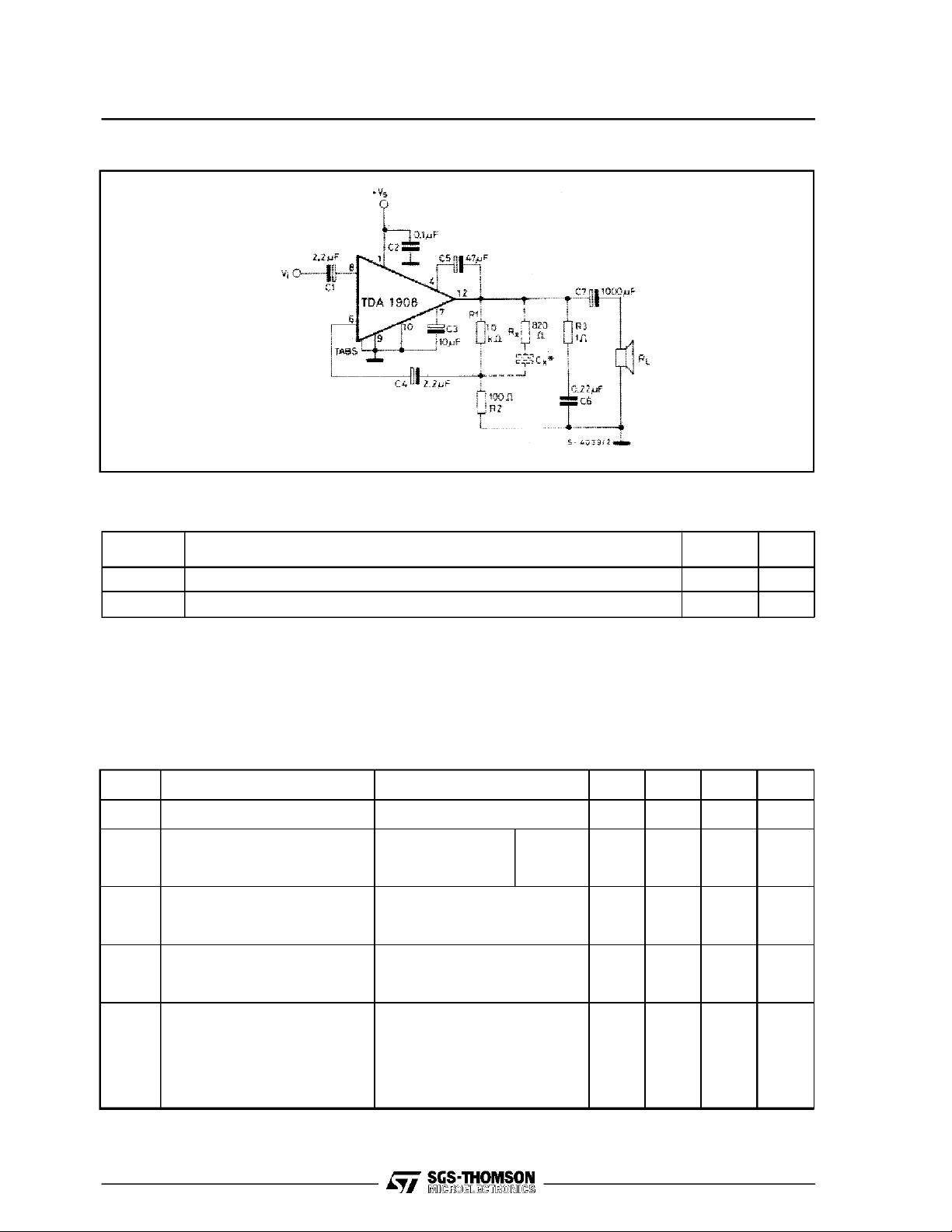
Figure19. Applicationcircuit with bootstrap
* R4 is necessary when Vsis less than 10V.
TDA1908
Figure 20. P.C. board and component lay-out of the circuit of fig. 19 (1 : 1 scale)
7/12
Page 8

TDA1908
APPLICATION INFORMATION (continued)
Figure 21. Application circuit without bootstrap
Figure22.Outputpowervs.
supply voltage (circuit of
fig. 21)
Figure 23. Position control for car headlights
8/12
Page 9

TDA1908
APPLICATION SUGGESTION
The recommendedvaluesof theexternal componentsarethoseshown on the applicationcircuit offig. 19.
Whenthe supplyvoltageVs is lessthan 10V, a 100Ω resistor mustbe connectedbetween pin1 andpin4
in order to obtain the maximum outputpower.
Different values can be used. The followingtable can help the designer.
Component
R
1
R
2
R
3
R
4
C
1
C
2
C
3
C
4
Raccom.
value
Purpose
10 KΩ Close loop gain
Larger than
raccomanded value
Increase of gain. Decrease of gain.
setting
100 Ω
Close loop gain
Decrease ofgain. Increase ofgain. R
setting.
1 Ω Frequency stability Danger of oscillation at
hight frequencies with
inductiveloads.
100 Ω
Increaseing of output
swing with low Vs.
2.2 µF
Input DC
Lower noise. Higher low
decoupling.
0,1 µF Supply voltage
bypass.
2.2 µF
10 µF
Inverting input DC
decoupling.
Ripple Rejection. Increase of SVR.
Increase of the
switch-on noise
Increase of the
switch-on time.
Smaller than
raccomanded value
Increase quiescent
current.
frequency cutoff.
Higher noise.
Danger of
oscillations.
Higher low
frequency cutoff.
Degradation of
SVR.
Allowed range
Min. Max.
9R
2
/9
1
47Ω 330 Ω
0.1 µF
0.1µF
2.2 µF 100 µF
C
5
47 µF Bootstrap Increase ofthe
10 mF 100 µF
distorsion at low
frequency
C
6
C
7
0.22 µF
1000 µF
Frequency stability. Danger of oscillation.
Output DC
decoupling.
Higher low
frequency cutoff.
9/12
Page 10

TDA1908
THERMALSHUT-DOWN
The presenceof a thermal limiting circuit offers the
followingadvantages:
1) An overload on the output (even if it is permanent),oranabovelimitambienttemperaturecan
be easily supported since the T
cannot be
j
higherthan 150°C.
2) The heatsinkcan have asmaller factor ofsafety
compared with that of a conventional circuit.
Thereis no possibilityof devicedamage dueto
high junction temperature.
Figure 24. Output power
and drain current vs.
case temperature
Figure 25. Output power
and d rain current vs.
case temperature
If, for any reason, the junction temperature increaseupto150°C, the thermal shut-downsimply reduces the power dissipation and the
currentconsumption.
The maximum allowable power dissipation depends uponthesizeof the externalheatsink(i.e. its
thermal resistance); fig. 25 shows the dissipable
power as a function of ambient temperature for
differentthermal resistance.
Fig ure 2 6. Max i mum
power dis sipat ion vs.
ambienttemperature
MOUNTINGINSTRUCTIONS
The thermalpower dissipatedin the circuitmay be
removedby solderingthe tabs to a copper area on
the PC board (see Fig. 27).
During soldering,tab temperaturemustnotexceed
260°C and the soldering time must not be longer
than 12 seconds.
Figure 27. Mounding example Figure 28. Maximum
power dissipation and
thermal resistance vs.
side””
10/12
Page 11

FINDIP PACKAGE MEHANICAL DATA
DIM.
MIN. TYP. MAX. MIN. TYP. MAX.
A 3.8 4.05 0.150 0.159
a1 1.5 1.75 0.059 0.069
b 0.55 0.6 0.022 0.024
b1 0.3 0.35 0.012 0.014
c 1.32 0.052
c1 0.94 0.037
D 19.2 19.9 0.756 0.783
E 16.8 17.2 17.6 0.661 0.677 0.693
E1 4.86 5.56 0.191 0.219
E2 10.11 10.81 0.398 0.426
e 2.29 2.54 2.79 0.090 0.100 0.110
e3 17.43 17.78 18.13 0.686 0.700 0.714
e4 7.62 0.300
e5 7.27 7.62 7.97 0.286 0.300 0.314
e6 12.35 12.7 13.05 0.486 0.500 0.514
F 6.3 7.1 0.248 0.280
F1 6.1 6.7 0.240 0.264
G 9.8 0.386
I 7.8 8.6 0.307 0.339
K 6.1 6.5 0.240 0.256
L 2.5 2.9 0.098 0.114
M 2.5 3.1 0.098 0.122
mm inch
TDA1908
K
b
c1
ce5
e6
e3
D
D1
12 7
G
e4
Aa1L
I
M
e
F
F1
61
E1
E2
E
FINDIP
b1
11/12
Page 12

TDA1908
Information furnished is believed to be accurate and reliable. However, SGS-THOMSON Microelectronics assumes no responsibility for the
consequences of use of such information nor for any infringement of patents or other rights of third parties which may result from its use. No
licenseis granted byimplication or otherwise under any patent or patent rights of SGS-THOMSON Microelectronics. Specifications mentioned
in this publication are subject to change without notice. This publication supersedes and replaces all information previously supplied.
SGS-THOMSON Microelectronics products are not authorized for use as critical componentsin life supportdevices or systems without express
written approval of SGS-THOMSON Microelectronics.
1994 SGS-THOMSON Microelectronics - All Rights Reserved
SGS-THOMSON Microelectronics GROUP OF COMPANIES
Australia - Brazil - France - Germany - Hong Kong - Italy- Japan - Korea -Malaysia - Malta - Morocco - The Netherlands - Singapore -
Spain - Sweden - Switzerland - Taiwan -Thaliand - UnitedKingdom - U.S.A.
12/12
 Loading...