

Page 1

INTEGRATED CIRCUITS
DATA SH EET
TDA1581T
Decoder for traffic warning (VWF)
radio transmissions
Preliminary specification
File under Integrated Circuits, IC01
March 1992
Page 2

Philips Semiconductors Preliminary specification
Decoder for traffic warning (VWF) radio
TDA1581T
transmissions
FEATURES
• Selective subcarrier amplifier (57 kHz) with gain control
• Transmitter identification signal (SK) decoder
• Area identification signal (BK) and announcement
identification signal (DK) active filtering
• BK and DK decoders (Schmitt trigger with switched
hysteresis)
• BK and DK switch-on/switch-off delay circuits
• SK and BK control outputs.
QUICK REFERENCE DATA
Measured in Fig.3 at V
C’ signal; or with f
m
= 8 mV; f = 57 kHz amplitude modulated with fm = 34.95 Hz and m = 60% for ‘BK-traffic area
iSK
= 125 Hz and m = 30% for DK signal
SYMBOL PARAMETER CONDITIONS MIN. TYP. MAX. UNIT
V
P
I
P
V
iSK
Z
i
V
iSK
V
i(p-p)
m
BKon
∆m
BK
t
dSKon
t
dSKoff
m
DKon
∆m
DK
t
dDKon
t
dDKoff
T
amb
supply voltage range 7.5 8.5 10 V
supply current − 6 − mA
nominal input voltage f = 57 kHz − 8 − mV
input impedance f ≤ 57 kHz 100 −−kΩ
control level −3 dB − 2.4 − mV
input voltage peak-to-peak value 2 −−V
SK switch-on threshold level − 42 − %
SK switch hysteresis − 3.5 − dB
SK switch-on delay − 150 − ms
SK switch-off delay − 750 − ms
DK switch-on threshold level − 13 − %
DK switch hysteresis − 3.6 − dB
DK switch-on delay − 750 − ms
DK switch-off delay − 750 − ms
operating ambient temperature range −30 − +80 °C
GENERAL DESCRIPTION
The TDA1581T decoder is for radio transmissions having
57 kHz amplitude-modulated subcarriers as used in the
german ‘Verkehrs Warnfunk’ (VWF) traffic warning
system.
ORDERING INFORMATION
PACKAGE
EXTENDED
TYPE NUMBER
PINS PIN POSITION MATERIAL CODE
TDA1581T 20 SO plastic SOT163A
Note
1. SOT163-1; 1996 August 28.
March 1992 2
(1)
Page 3
Philips Semiconductors Preliminary specification
Decoder for traffic warning (VWF) radio
transmissions
TDA1581T
March 1992 3
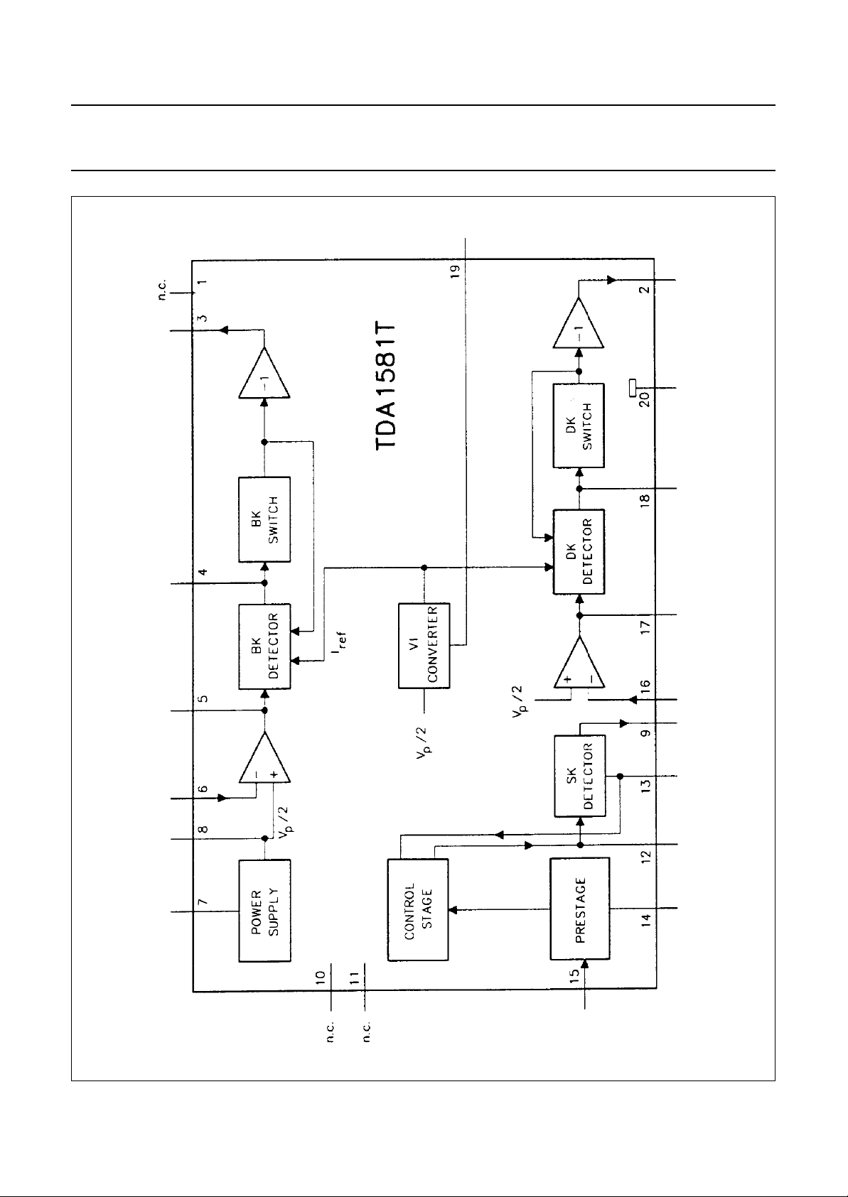
Fig.1 Block diagram.
Page 4
Philips Semiconductors Preliminary specification
Decoder for traffic warning (VWF) radio
transmissions
PINNING
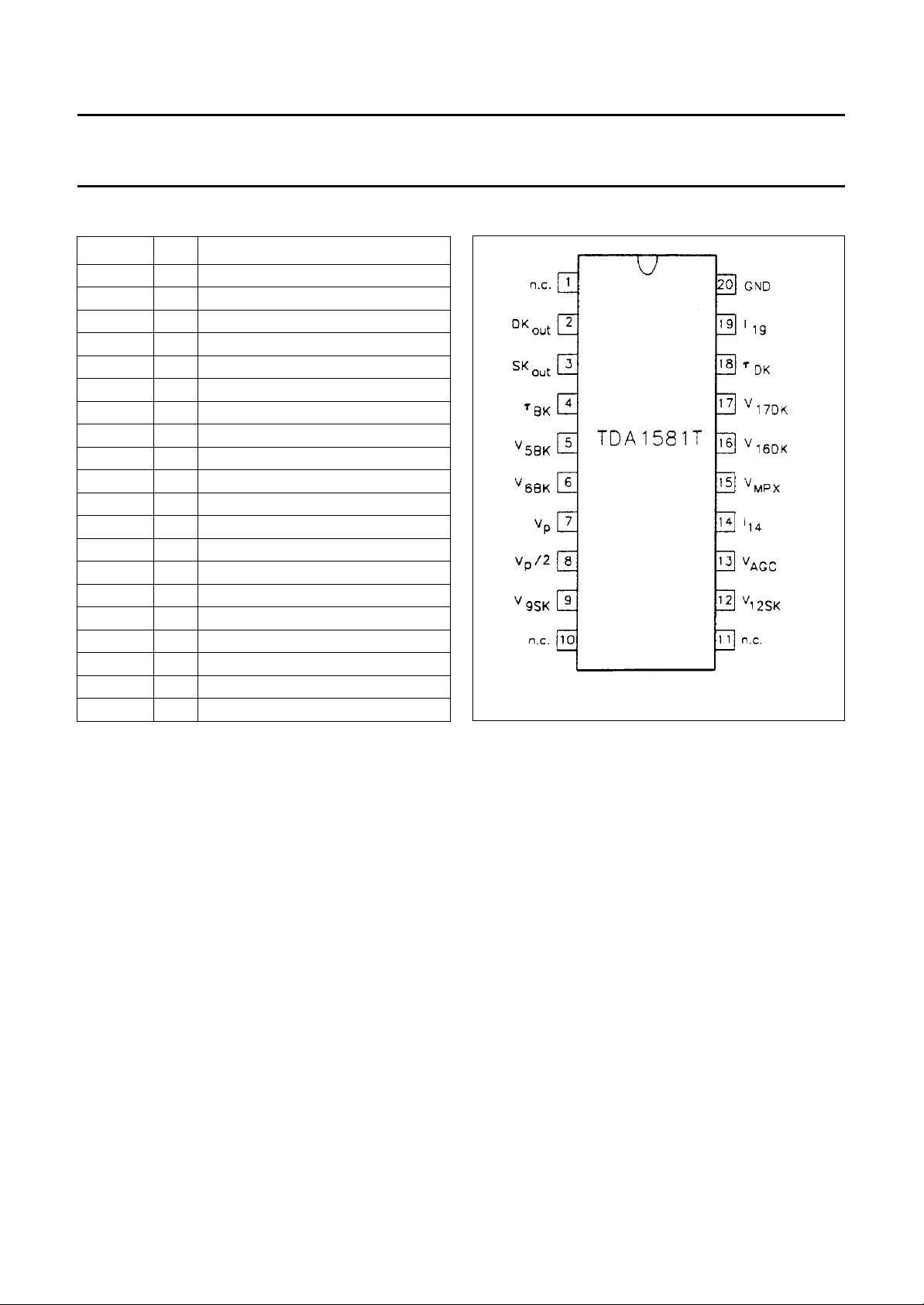
SYMBOL PIN DESCRIPTION
n.c. 1 not connected
DK
out
SK
out
τ
BK
V
5BK
V
6BK
V
P
/ 2 8 half supply voltage
V
P
V
9SK
n.c. 10 not connected
n.c. 11 not connected
V
12SK
V
AGC
I
14
V
MPX
V
16DK
V
17DK
τ
DK
I
19
GND 20 ground
2 DK output current
3 SK output current
4 time delay BK
5 filter output BK
6 filter input BK
7 supply voltage
9 SK detector output
12 57 kHz band pass filter
13 AGC
14 prestage biasing current
15 MPX input
16 filter input DK
17 filter output DK
18 time delay DK
19 reference current for BK, DK detector
TDA1581T
Fig.2 Pin configuration.
March 1992 4
Page 5

Philips Semiconductors Preliminary specification
Decoder for traffic warning (VWF) radio
TDA1581T
transmissions
LIMITING VALUES
In accordance with the Absolute Maximum System (IEC134).
SYMBOL PARAMETER CONDITIONS MIN. TYP. MAX. UNIT
= V
V
P
7-20
V
2; 3-20
I
2; 3
V
15-20
I
15
P
tot
T
stg
T
amb
CHARACTERISTICS
= 8.5 V; T
V
p
= 34.95 Hz and m = 60% for ‘BK-traffic area C’ signal; or with fm = 125 Hz and m = 30% for DK signal.
f
m
SYMBOL PARAMETER CONDITIONS MIN. TYP. MAX. UNIT
V
P
I
P
SK amplifier/decoder
Z
i
V
i(p-p)
V
iSK
G
v9-15
∆G
v9-15
∆G
v
V
o9BK
V
o9DK
BK circuit
V
o5BKon
V
o5BKon
--------------------- V
o5BKoff
V
4-20off
I
3
V
3-20sat
V
3-20
supply voltage pin 7 −−15 V
switch output voltage pins 2 or 3 −0.5 − 15 V
switch output current pins 2 or 3 −10 − 5mA
signal input voltage pin 15 −0.5 − V
P
signal input current pin 15 −−−10 mA
total power dissipation −−800 mW
storage temperature range −55 − +150 °C
operating ambient temperature range −30 − +80 °C
= +25 °C; measured at nominal input signal: V
amb
= 8 mV, f = 57 kHz amplitude modulated with
iSK
supply voltage pin 7 7.5 − 10 V
supply current pin 7 − 615mA
input impedance f ≤ 57 kHz 60 −−kΩ
input voltage (peak-to-peak value) 2 −−V
input voltage at start of gain control V
voltage gain V
= −3 dB − 2.4
o9BK
9BK
/ V
15SK
− 44
(1)
(1)
− mV
− dB
gain spread −−±2dB
gain control range 40 −−dB
controlled output voltage − 440 − mV
− 220 − mV
switch-on threshold level pin 3 high-Z 600 670 750 mV
switch hysteresis 3 3.5 4 dB
BK switch threshold level for BK-off
(SK-off) (typ. value = 0.21V
8-20
)
pin 3 conducting 0.8 0.88 0.97 V
SK output (pin 3)
permitted load current −−0.5 mA
saturation voltage I3 = 1.5 mA −−0.35 V
rejection voltage I3<5µA18−−V
V
March 1992 5
Page 6

Philips Semiconductors Preliminary specification
Decoder for traffic warning (VWF) radio
TDA1581T
transmissions
SYMBOL PARAMETER CONDITIONS MIN. TYP. MAX. UNIT
DK circuit
V
17DKon
V
17DKon
--------------------- V
17DKoff
V
18-20off
I
2
V
2-20sat
V
2-20
BK and DK filter amplifiers
G
o
G
i
I
i
V
o5-8
V
17-8
I
o
R
o
C
L
Internal reference voltage
V
8-20
R
8
I
8-20
I
20-8
I
8sc
switch-on threshold level pin 2 high-Z 600 670 750 mV
switch hysteresis 3.1 3.6 4.1 dB
DK switch threshold level for DK-off
pin 2 conducting − 0.6 − V
(Schmitt trigger output)
(typ. value = 1 × VBE)
DK output (pin 2)
permitted load current −−0.5 mA
saturation voltage I2 = 1.5 mA −−0.35 V
rejection voltage I2<5µA18−−V
open loop gain f = 100 Hz 84 −−dB
current gain 120 −−dB
input bias current −−±50 nA
output offset voltage R
5-6
= R
= 680 kΩ− − ±50 mV
16-17
available output current ±1 −−mA
output resistance − 2 3.5 kΩ
permitted load capacitance −−50 pF
output voltage (typ. value = 0.5VP) 4.0 4.25 4.5 V
internal resistance of voltage source −−5Ω
available output current −2 −−mA
0.6 −−mA
output short-circuit current
−−8−mA
(typ. value = VP/1 kΩ)
Reference current source
V
R
R
19-20
i19
19-20
reference voltage
(typ. value = V
8-20
− VBE)
internal biasing resistor − 5 − kΩ
permitted range of external
reference resistor
Note
1. selectable by R
14-8
or Z
12-8
.
March 1992 6
− 3.6 − V
180 − 270 kΩ
Page 7

Philips Semiconductors Preliminary specification
Decoder for traffic warning (VWF) radio
TDA1581T
transmissions
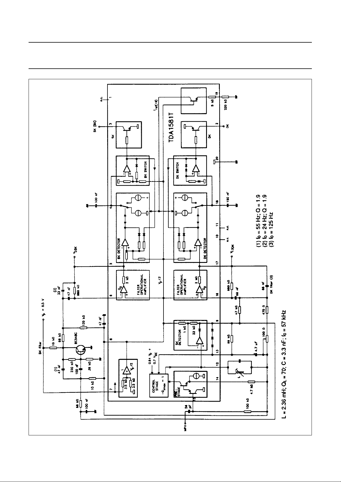
APPLICATION INFORMATION (see Fig.3)
SYMBOL PARAMETER CONDITIONS MIN. TYP. MAX. UNIT
V
iSKon
m
BKon
m
BKon
----------------m
BKoff
t
dSKon
t
dSKoff
V
iDKon
m
DKon
m
DKon
----------------m
DKoff
t
dDKon
t
dDKoff
Notes to the application information
1. Sequence for measuring switch-on delay times (t
a) Nominal BK or DK input signal at pin 15: V
b) Pin 4 of the BK detector (pin 18 of the DK detector) is switched to ground to cause a low signal at the SK output
at pin 3 (DK output at pin 2).
c) t
commences when the ground connection is removed from pin 4 (pin 18) as the positive-going V
don
pin 5 (V
t
ends when the positive-going edge of the SK output arrives at pin 15 (DK at pin 2).
don
2. Sequence for measuring switch-off delay times (t
a) Nominal operating conditions as in note 1.
b) t
commences when the input is switched off as the negative-going V
doff
crosses zero.
t
ends when the negative-going edge of the SK output arrives at pin 3 (DK at pin 2).
doff
SK switch-on threshold level mBK = 60 % − 1.8 − mV
SK switch-on threshold level V
= 8 mV − 32 − %
iSK
SK switch hysteresis 3.0 3.5 4.0 dB
SK switch-on delay note 1 − 95 200 ms
SK switch-off delay note 2 380 500 700 ms
DK switch-on threshold level mDK = 30 % − 1.5 − mV
DK switch-on threshold level V
= 8 mV − 13 − %
iDK
DK switch hysteresis 3.1 3.6 4.1 dB
DK switch-on delay note 1 − 750 1000 ms
DK switch-off delay note 2 600 750 1000 ms
)
don
= 8 mV; f = 57 kHz; modulation-on.
i(p-p)
signal at pin 17) crosses zero.
oDK
)
doff
signal at pin 5 (V
oBK
signal at pin 17)
oDK
oBK
signal at
March 1992 7
Page 8
Philips Semiconductors Preliminary specification
Decoder for traffic warning (VWF) radio
transmissions
TDA1581T
March 1992 8
Fig.3 Application diagram.
Page 9
Philips Semiconductors Preliminary specification
Decoder for traffic warning (VWF) radio
transmissions
TDA1581T
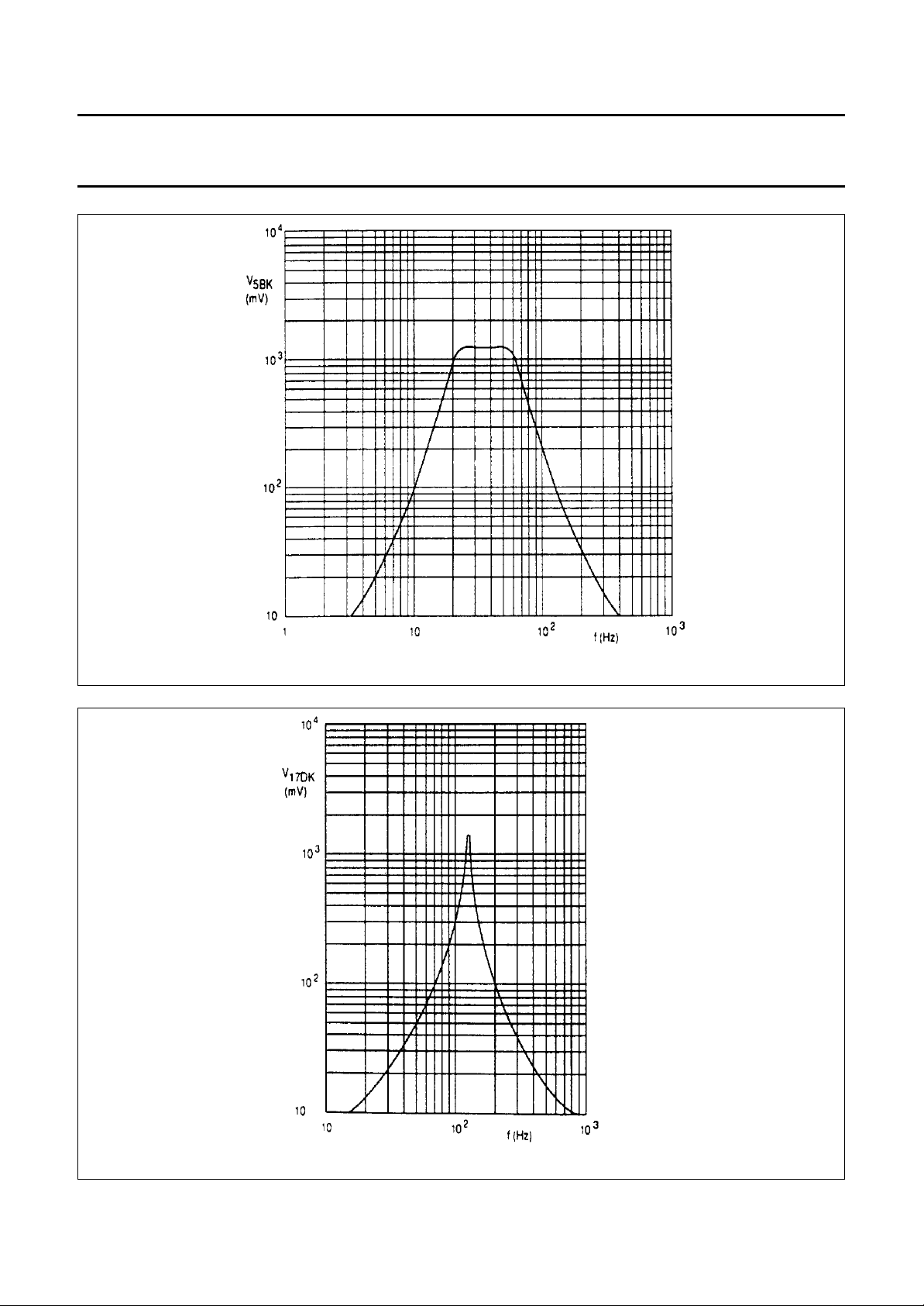
Fig.4 BK signal voltage at pin 5 as a function of frequency.
Fig.5 DK signal voltage at pin 17 as a function of frequency: f0 = 125 Hz; Q ≈ 18.
March 1992 9
Page 10
Philips Semiconductors Preliminary specification
Decoder for traffic warning (VWF) radio
transmissions
TDA1581T
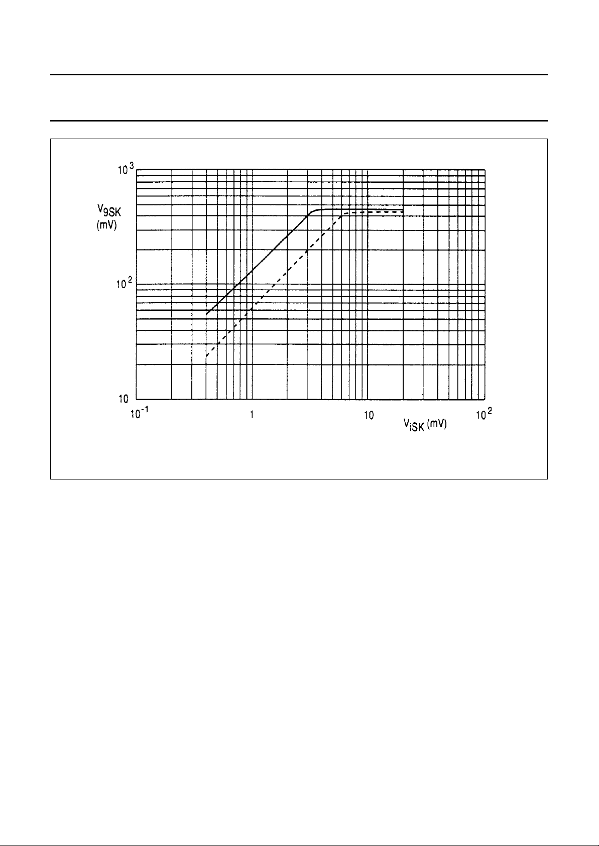
Fig.6 Control characteristic of the SK amplifier at VP = 8.5 V, mBK = 60% and QL = 70.
March 1992 10
Page 11
Philips Semiconductors Preliminary specification
Decoder for traffic warning (VWF) radio
transmissions
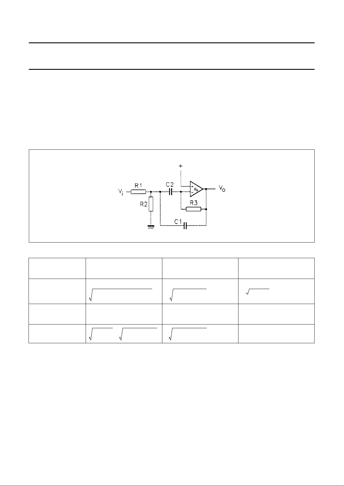
FILTER INFORMATION
Gain
Amplifier conditions: G
G
-----------------------------------------------------------------------------------------------------------------------------------
v
2
p
C1 C2+
p
------------------------------------ R3 C1 C2××
>> Gvand Go>> 2 × Q
o
p
---------------------R1 C1×
+×+
----------------------------------------------------------------R1 R2 R3 C1 C2××××
2
R1 R2+
, in which
pjωand G
TDA1581T
V
o
==–=
------
v
V
i
GENERAL EQUATION C1 = C2 = C C1 = C2 = C
resonance frequency
ω
=
r
gain at ω = ω
r
−Gvr=
quality
Q =
--------------------------------------------------------------------- R1 R2×
---------------------R1 R2+
C2
----------------------
C1 C2+
C1 C2×
---------------------C1 C2+
1
R3 C1 C2×××
R3
×
------- R1
R3 R1 R2+()
------------------------------------- -×
R1 R2×
--------------------------------------------- C
1
-- 2
1
-- 2
1
R1 R2×
---------------------R1 R2+
R3
×
------- R1
R3 R1 R2+()
------------------------------------- R1 R2×
R3×
Recommended components
C1, C2 metallized polycarbonate film (MKC) capacitors; ±5%
and
R1, R2, R3 metal film (MR) resistors; ±2%
or
C1, C2 metallized polyester film (MKT) capacitors; ±5%
and
R1, R2, R3 carbon film (CR) resistors; ±2%
1
------------------------------CR2 R3×
R3
1
×
------- -
-- R1
2
1
R3
×
-- -
------- -
2
R2
R2 << R1
March 1992 11
Page 12
Philips Semiconductors Preliminary specification
Decoder for traffic warning (VWF) radio
transmissions
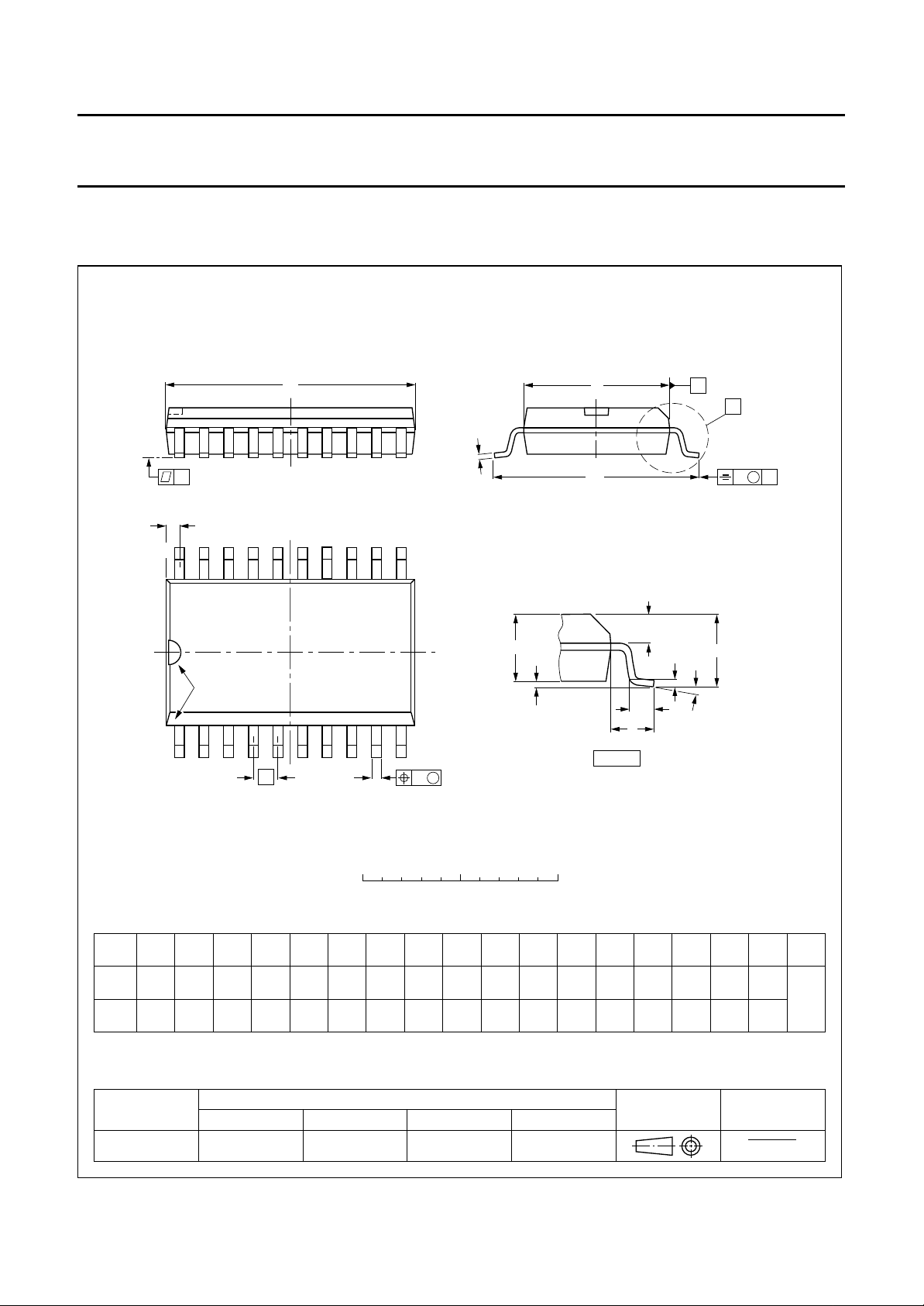
PACKAGE OUTLINE
SO20: plastic small outline package; 20 leads; body width 7.5 mm
D
c
y
Z
20
11
TDA1581T
SOT163-1
E
H
E
A
X
v M
A
pin 1 index
1
e
0 5 10 mm
DIMENSIONS (inch dimensions are derived from the original mm dimensions)
mm
A
max.
2.65
0.10
A
1
0.30
0.10
0.012
0.004
A2A
2.45
2.25
0.096
0.089
0.25
0.01
b
p
cD
0.32
0.23
0.013
0.009
3
0.49
0.36
0.019
0.014
UNIT
inches
Note
1. Plastic or metal protrusions of 0.15 mm maximum per side are not included.
10
w M
b
p
scale
(1)E(1) (1)
13.0
12.6
0.51
0.49
eHELLpQ
7.6
1.27
7.4
0.30
0.050
0.29
10.65
10.00
0.42
0.39
Q
A
2
A
1
1.4
0.055
1.1
0.4
0.043
0.016
detail X
1.1
1.0
0.043
0.039
(A )
L
p
L
0.25
0.01
A
3
θ
0.25 0.1
0.01
ywv θ
Z
0.9
0.4
8
0.004
0.035
0.016
0
o
o
OUTLINE
VERSION
SOT163-1
IEC JEDEC EIAJ
075E04 MS-013AC
REFERENCES
March 1992 12
EUROPEAN
PROJECTION
ISSUE DATE
92-11-17
95-01-24
Page 13

Philips Semiconductors Preliminary specification
Decoder for traffic warning (VWF) radio
transmissions
SOLDERING
Introduction
There is no soldering method that is ideal for all IC
packages. Wave soldering is often preferred when
through-hole and surface mounted components are mixed
on one printed-circuit board. However, wave soldering is
not always suitable for surface mounted ICs, or for
printed-circuits with high population densities. In these
situations reflow soldering is often used.
This text gives a very brief insight to a complex technology.
A more in-depth account of soldering ICs can be found in
“IC Package Databook”
our
Reflow soldering
Reflow soldering techniques are suitable for all SO
packages.
Reflow soldering requires solder paste (a suspension of
fine solder particles, flux and binding agent) to be applied
to the printed-circuit board by screen printing, stencilling or
pressure-syringe dispensing before package placement.
(order code 9398 652 90011).
TDA1581T
Maximum permissible solder temperature is 260 °C, and
maximum duration of package immersion in solder is
10 seconds, if cooled to less than 150 °C within
6 seconds. Typical dwell time is 4 seconds at 250 °C.
A mildly-activated flux will eliminate the need for removal
of corrosive residues in most applications.
Repairing soldered joints
Fix the component by first soldering two diagonallyopposite end leads. Use only a low voltage soldering iron
(less than 24 V) applied to the flat part of the lead. Contact
time must be limited to 10 seconds at up to 300 °C. When
using a dedicated tool, all other leads can be soldered in
one operation within 2 to 5 seconds between
270 and 320 °C.
Several techniques exist for reflowing; for example,
thermal conduction by heated belt. Dwell times vary
between 50 and 300 seconds depending on heating
method. Typical reflow temperatures range from
215 to 250 °C.
Preheating is necessary to dry the paste and evaporate
the binding agent. Preheating duration: 45 minutes at
45 °C.
Wave soldering
Wave soldering techniques can be used for all SO
packages if the following conditions are observed:
• A double-wave (a turbulent wave with high upward
pressure followed by a smooth laminar wave) soldering
technique should be used.
• The longitudinal axis of the package footprint must be
parallel to the solder flow.
• The package footprint must incorporate solder thieves at
the downstream end.
During placement and before soldering, the package must
be fixed with a droplet of adhesive. The adhesive can be
applied by screen printing, pin transfer or syringe
dispensing. The package can be soldered after the
adhesive is cured.
March 1992 13
Page 14

Philips Semiconductors Preliminary specification
Decoder for traffic warning (VWF) radio
TDA1581T
transmissions
DEFINITIONS
Data sheet status
Objective specification This data sheet contains target or goal specifications for product development.
Preliminary specification This data sheet contains preliminary data; supplementary data may be published later.
Product specification This data sheet contains final product specifications.
Limiting values
Limiting values given are in accordance with the Absolute Maximum Rating System (IEC 134). Stress above one or
more of the limiting values may cause permanent damage to the device. These are stress ratings only and operation
of the device at these or at any other conditions above those given in the Characteristics sections of the specification
is not implied. Exposure to limiting values for extended periods may affect device reliability.
Application information
Where application information is given, it is advisory and does not form part of the specification.
LIFE SUPPORT APPLICATIONS
These products are not designed for use in life support appliances, devices, or systems where malfunction of these
products can reasonably be expected to result in personal injury. Philips customers using or selling these products for
use in such applications do so at their own risk and agree to fully indemnify Philips for any damages resulting from such
improper use or sale.
March 1992 14
 Loading...