

Page 1

INTEGRATED CIRCUITS
DATA SH EET
TDA1519C
22 W BTL or 2 × 11 W
stereo power amplifier
Product specification
Supersedes data of 2000 Mar 08
File under Integrated Circuits, IC01
2001 Aug 24
Page 2

Philips Semiconductors Product specification
22 W BTL or 2 × 11 W
stereo power amplifier
FEATURES
• Requires very fewexternal components for Bridge-Tied
Load (BTL) operation
• Stereo or BTL application
• High output power
• Low offset voltage at output (important for BTL
applications)
• Fixed gain
• Good ripple rejection
• Mute/standby switch
• Load dump protection
• AC and DC short-circuit safe to ground and V
• Thermally protected
• Reverse polarity safe
• Capability to handle high energy on outputs (VP=0V)
• No switch-on/switch-off plops
• Protected against electrostatic discharge
• Low thermal resistance
• Identical inputs (inverting and non-inverting)
• Pin compatible with TDA1519B (TDA1519C and
TDA1519CSP).
P
TDA1519C
GENERAL DESCRIPTION
The TDA1519C is an integrated class-B dual output
amplifierin a 9-leadplastic single in-linepower package or
20-lead heatsink small outline package.
For the TDA1519CTH (SOT418-2), the heatsink is
positioned on top of the package,which allows anexternal
heatsink to be mounted on top. The heatsink of the
TDA1519CTD (SOT397-1) is facing the PCB, allowing the
heatsink to be soldered onto the copper area of the PCB.
ORDERING INFORMATION
TYPE NUMBER
NAME DESCRIPTION VERSION
TDA1519C SIL9P plastic single in-line power package; 9 leads SOT131-2
TDA1519CSP SMS9P plastic surface mounted single in-line power package; 9 leads SOT354-1
TDA1519CTD HSOP20 plastic, heatsink small outline package; 20 leads SOT397-1
TDA1519CTH HSOP20 plastic, heatsink small outline package; 20 leads; low stand-off height SOT418-2
PACKAGE
2001 Aug 24 2
Page 3

Philips Semiconductors Product specification
22 W BTL or 2 × 11 W
TDA1519C
stereo power amplifier
QUICK REFERENCE DATA
SYMBOL PARAMETER CONDITIONS MIN. TYP. MAX. UNIT
Supply
V
P
I
ORM
I
q(tot)
I
stb
I
sw(on)
Inputs
input impedance BTL 25 −−kΩ
Z
i
Stereo application
P
o
α
cs
V
n(o)(rms)
BTL application
P
o
SVRR supply voltage ripple rejection R
∆V
DC output offset voltage −−250 mV
OO
T
j
supply voltage operating 6.0 14.4 17.5 V
non-operating −−30 V
load dump protected −−45 V
repetitive peak output current −−4A
total quiescent current − 40 80 mA
standby current − 0.1 100 µA
switch-on current −−40 µA
stereo 50 −−kΩ
output power THD = 10%
=4Ω−6−W
R
L
R
=2Ω−11 − W
L
channel separation 40 −−dB
noise output voltage (RMS value) − 150 −µV
output power THD = 10%; RL=4Ω−22 − W
=0Ω
S
f
= 100 Hz 34 −−dB
i
f
= 1 to 10 kHz 48 −−dB
i
junction temperature −−150 °C
2001 Aug 24 3
Page 4

Philips Semiconductors Product specification
22 W BTL or 2 × 11 W
stereo power amplifier
BLOCK DIAGRAM
handbook, full pagewidth
NINV
RR
TDA1519C
switch
VA
15 kΩ
15 kΩ
mute switch
VA
18.1 kΩ
V
P
18.1 kΩ
C
m
+
+
−
mute
reference
voltage
power stage
+
−
TDA1519C
TDA1519CSP
standby
reference
voltage
mute
switch
4
OUT1
8
M/SS
1
60
kΩ
183
Ω
standby
× 1
3
power stage
183
Ω
9
INV
60
kΩ
input
reference
voltage
GND1 GND2V
The pin numbers refer to the TDA1519C and TDA1519CSP only, for TDA1519CTD and TDA1519CTH see Figs 3 and 4.
VA
C
m
mute switch
signal
ground
2 7
power
ground
(substrate)
5
P
6
MGL491
Fig.1 Block diagram.
2001 Aug 24 4
OUT2
Page 5
Philips Semiconductors Product specification
22 W BTL or 2 × 11 W
TDA1519C
stereo power amplifier
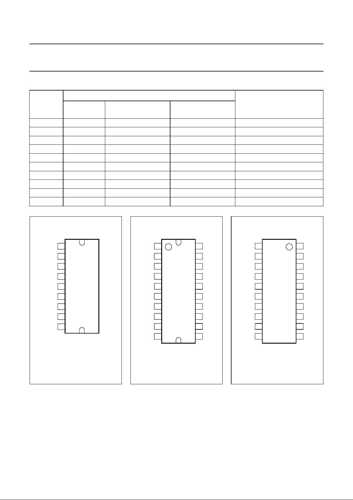
PINNING
PIN
SYMBOL
TDA1519C;
TDA1519CSP
TDA1519CTD TDA1519CTH
NINV 1 19 19 non-inverting input
GND1 2 20 20 ground 1 (signal)
RR 3 1 1 supply voltage ripple rejection
OUT1 4 3 3 output 1
GND2 5 5 5 ground 2 (substrate)
OUT2 6 8 8 output 2
V
P
7 10 10 positive supply voltage
M/SS 8 11 11 mute/standby switch input
INV 9 12 12 inverting input
n.c. − 2, 4, 6, 7, 9 and 13 to 18 2, 4, 6, 7, 9 and 13 to 18 not connected
DESCRIPTION
alfpage
NINV
GND1
RR
OUT1
GND2
OUT2
V
M/SS
INV
1
2
3
4
5
6
7
P
8
9
TDA1519C
TDA1519CSP
Fig.2 Pin configuration
TDA1519C and
TDA1519CSP.
MGR561
page
RR
n.c.
OUT1
n.c.
GND2
n.c.
n.c.
OUT2
n.c.
V
1
2
3
4
5
6
7
8
9
10
P
TDA1519CTD
Fig.3 Pin configuration
TDA1519CTD.
MGL937
GND1
20
19
NINV
18
n.c.
17
n.c.
16
n.c.
15
n.c.
n.c.
14
n.c.
13
INV
12
M/SS
11
page
GND1
NINV
n.c.
n.c.
n.c.
n.c.
n.c.
n.c.
INV
M/SS
20
19
18
17
16
TDA1519CTH
15
14
13
12
11
MGL936
RR
1
n.c.
2
OUT1
3
n.c.
4
GND2
5
n.c.
6
n.c.
7
8
OUT2
n.c.
9
V
10
P
Fig.4 Pin configuration
TDA1519CTH.
2001 Aug 24 5
Page 6
Philips Semiconductors Product specification
22 W BTL or 2 × 11 W
TDA1519C
stereo power amplifier
FUNCTIONAL DESCRIPTION
The TDA1519C contains two identical amplifiers with
differential input stages. The gain of each amplifier isfixed
at 40 dB. A special feature of this device is the
mute/standby switch which has the following features:
LIMITING VALUES
In accordance with the Absolute Maximum Rating System (IEC 60134).
SYMBOL PARAMETER CONDITIONS MIN. MAX. UNIT
V
P
V
sc
V
rp
E
o
I
OSM
I
ORM
P
tot
T
j
T
stg
supply voltage operating − 17.5 V
AC and DC short-circuit-safe voltage − 17.5 V
reverse polarity voltage − 6V
energy handling capability at outputs VP=0V − 200 mJ
non-repetitive peak output current − 6A
repetitive peak output current − 4A
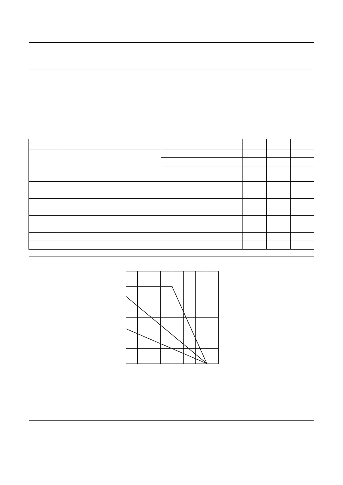
total power dissipation see Fig.5 − 25 W
junction temperature − 150 °C
storage temperature −55 +150 °C
• Low standby current (<100 µA)
• Low mute/standby switching current (allows for low-cost
supply switch)
• Mute condition.
non-operating − 30 V
load dump protected;
− 45 V
during 50 ms; tr≥ 2.5 ms
(1) Infinite heatsink.
(2) R
(3) R
th(c-a)
th(c-a)
= 5 K/W.
= 13 K/W.
30
handbook, halfpage
P
tot
(W)
20
10
0
−25 0 50 150
(1)
(2)
(3)
100
T
Fig.5 Power derating curve for TDA1519C.
amb
MGL492
(°C)
2001 Aug 24 6
Page 7

Philips Semiconductors Product specification
22 W BTL or 2 × 11 W
TDA1519C
stereo power amplifier
THERMAL CHARACTERISTICS
SYMBOL PARAMETER CONDITIONS VALUE UNIT
R
th(j-a)
thermal resistance from junction to ambient;
TDA1519C, TDA1519CTH and TDA1519CTD
R
th(j-c)
thermal resistance from junction to case;
TDA1519C, TDA1519CTH and TDA1519CTD
DC CHARACTERISTICS
VP= 14.4 V; T
=25°C; measured in circuit of Fig.6; unless otherwise specified.
amb
SYMBOL PARAMETER CONDITIONS MIN. TYP. MAX. UNIT
Supply
V
P
I
q(tot)
V
O
∆V
OO
supply voltage note 1 6.0 14.4 17.5 V
total quiescent current − 40 80 mA
DC output voltage note 2 − 6.95 − V
DC output offset voltage −−250 mV
Mute/standby switch
V
sw(on)
V
mute
V
stb
switch-on voltage level 8.5 −−V
mute voltage level 3.3 − 6.4 V
standby voltage level 0 − 2V
Mute/standby condition
V
o
output voltage mute mode; Vi= 1 V (maximum);
fi=20Hzto15kHz
∆V
DC output offset voltage mute mode −−250 mV
OO
I
stb
I
sw(on)
standby current standby mode −−100 µA
switch-on current − 12 40 µA
in free air 40 K/W
3 K/W
−−20 mV
Notes
1. The circuit is DC adjusted at V
= 6 to 17.5 V and AC operating at VP= 8.5 to 17.5 V.
P
2. At VP= 17.5 to 30 V, the DC output voltage is ≤0.5VP.
2001 Aug 24 7
Page 8

Philips Semiconductors Product specification
22 W BTL or 2 × 11 W
TDA1519C
stereo power amplifier
AC CHARACTERISTICS
VP= 14.4 V; RL=4Ω; f = 1 kHz; T
SYMBOL PARAMETER CONDITIONS MIN. TYP. MAX. UNIT
Stereo application (see Fig.6)
P
o
output power note 1
THD total harmonic distortion P
f
ro(l)
f
ro(h)
G
v(cl)
low frequency roll-off −3 dB; note 2 − 45 − Hz
high frequency roll-off −1dB 20 −−kHz
closed-loop voltage gain 39 40 41 dB
SVRR supply voltage ripple rejection on; notes 3 and 4 40 −−dB
Z
input impedance 50 60 75 kΩ
i
V
n(o)(rms)
α
cs
∆G
noise output voltage (RMS value) note 7
channel separation RS=10kΩ 40 −−dB
channel unbalance − 0.1 1 dB
v(ub)
BTL application (see Fig.7)
P
o
output power note 1
THD total harmonic distortion P
B
f
ro(l)
f
ro(h)
G
p
v(cl)
power bandwidth THD = 0.5%;
low frequency roll-off −1 dB; note 2 − 45 − Hz
high frequency roll-off −1dB 20 −−kHz
closed-loop voltage gain 45 46 47 dB
=25°C; unless otherwise specified.
amb
THD = 0.5% 4 5 − W
THD = 10% 5.5 6.0 − W
R
=2Ω; note 1
L
THD = 0.5% 7.5 8.5 − W
THD = 10% 10 11 − W
=1W − 0.1 − %
o
on; notes 3 and 5 45 −−dB
mute; notes 3 and 6 45 −−dB
standby; notes 3
and 6
on; R
=0Ω−150 −µV
S
=10kΩ− 250 500 µV
on; R
S
mute; note 8 − 120 −µV
THD = 0.5% 15 17 − W
THD = 10% 20 22 − W
V
= 13.2 V; note 1
P
THD = 0.5% − 13 − W
THD = 10% − 17.5 − W
=1W − 0.1 − %
o
Po= −1 dB; with
respect to 15 W
80 −−dB
− 35 to 15000 − Hz
2001 Aug 24 8
Page 9

Philips Semiconductors Product specification
22 W BTL or 2 × 11 W
TDA1519C
stereo power amplifier
SYMBOL PARAMETER CONDITIONS MIN. TYP. MAX. UNIT
SVRR supply voltage ripple rejection on; notes 3 and 4 34 −−dB
on; notes 3 and 5 48 −−dB
mute; notes 3 and 6 48 −−dB
standby;
notes 3 and 6
Z
input impedance 25 30 38 kΩ
i
V
n(o)(rms)
Notes
1. Output power is measured directly at the output pins of the device.
2. Frequency response externally fixed.
3. Ripple rejection measured at the output with a source impedance of 0 Ω (maximum ripple amplitude of 2 V).
4. Frequency f = 100 Hz.
5. Frequency between 1 and 10 kHz.
6. Frequency between 100 Hz and 10 kHz.
7. Noise voltage measured in a bandwidth of 20 Hz to 20 kHz.
8. Noise output voltage independent of RS (Vi= 0 V).
noise output voltage (RMS value) note 7
on; R
on; R
mute; note 8 − 180 −µV
=0Ω−200 −µV
S
=10kΩ− 350 700 µV
S
80 −−dB
2001 Aug 24 9
Page 10
Philips Semiconductors Product specification
22 W BTL or 2 × 11 W
stereo power amplifier
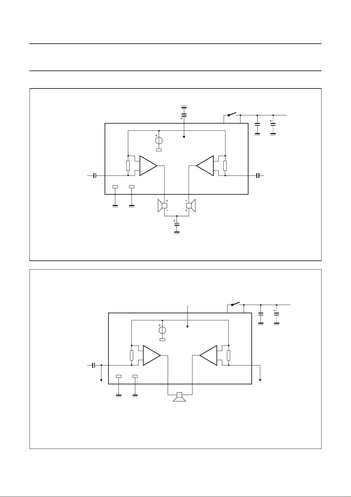
APPLICATION INFORMATION
handbook, full pagewidth
220 nF
60 kΩ
1
signal
ground
38
input
reference
voltage
−
40 dB
+
546
2
power
ground
internal
1/2 V
TDA1519C
1000
µF
100 µF
P
40 dB
standby switch
+
−
7
60 kΩ
9
MGL493
220 nF
TDA1519C
2200
100
nF
µF
inverting inputnon-inverting input
V
P
handbook, full pagewidth
non-inverting input
220 nF
to pin 9
Fig.6 Stereo application diagram (TDA1519C).
38
input
1
signal
ground
60 kΩ
2
reference
voltage
−
40 dB
+
546
power
ground
internal
1/2 V
TDA1519C
RL = 4 Ω
P
+
40 dB
−
standby switch
7
60 kΩ
MGL494
V
P
2200
100
nF
9
to pin 1
µF
Fig.7 BTL application diagram (TDA1519C).
2001 Aug 24 10
Page 11
Philips Semiconductors Product specification
22 W BTL or 2 × 11 W
stereo power amplifier
handbook, halfpage
TDA1519C
60
I
q(tot)
(mA)
50
40
30
020
4 8 12 16
MGR539
VP (V)
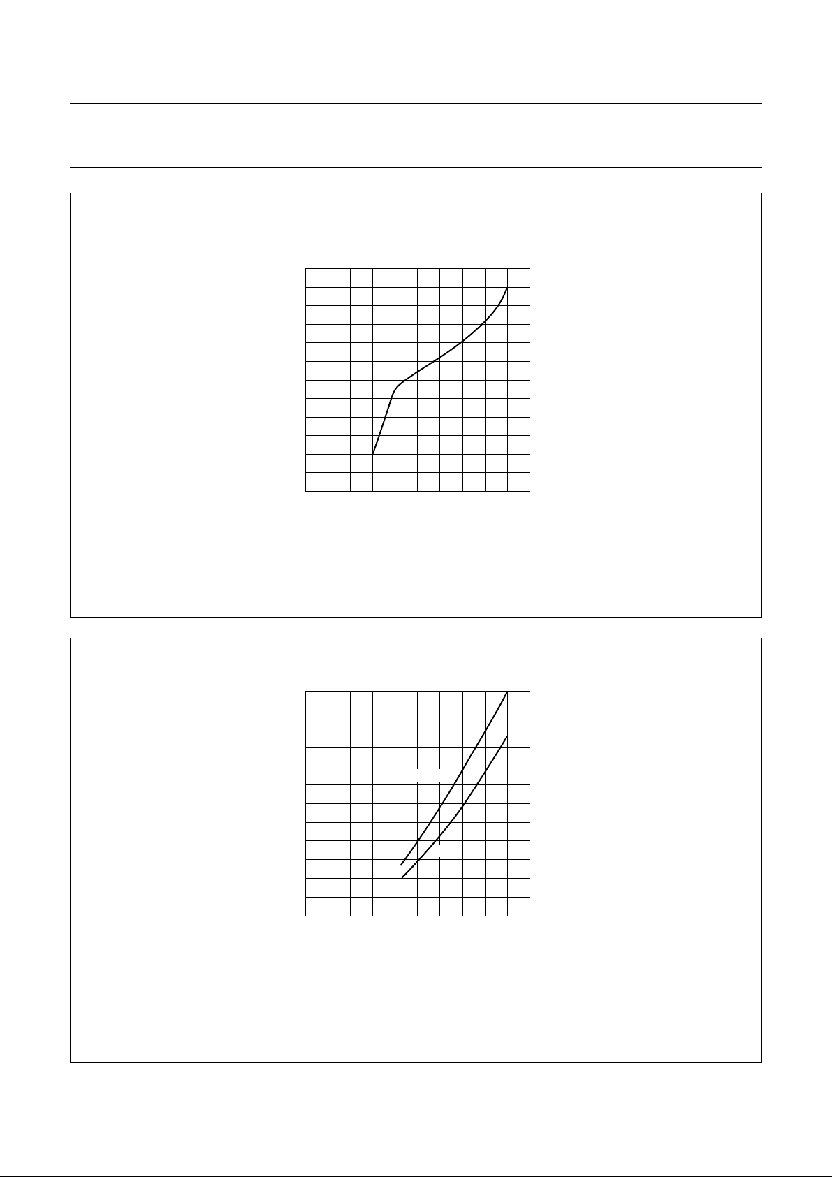
BTL application.
=4Ω.
R
L
fi= 1 kHz.
Fig.8 Total quiescent current as a function of the supply voltage.
30
handbook, halfpage
P
o
(W)
20
10
0
020
THD = 10%
0.5%
4 8 12 16
MGR540
VP (V)
Fig.9 Output power as a function of the supply voltage.
2001 Aug 24 11
Page 12
Philips Semiconductors Product specification
22 W BTL or 2 × 11 W
stereo power amplifier
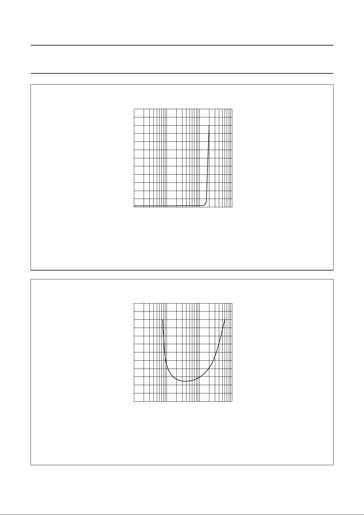
handbook, halfpage
THD
(%)
TDA1519C
Po (W)
MGR541
2
12
8
4
0
−1
10
11010
BTL application.
R
=4Ω.
L
fi= 1 kHz.
Fig.10 Total harmonic distortion as a function of the output power.
0.6
handbook, halfpage
THD
(%)
0.4
0.2
0
10 10
2
10
MGU377
3
fi (Hz)
4
10
BTL application.
RL=4Ω.
Po=1W.
Fig.11 Total harmonic distortion as a function of the operating frequency.
2001 Aug 24 12
Page 13
Philips Semiconductors Product specification
22 W BTL or 2 × 11 W
stereo power amplifier
PACKAGE OUTLINES
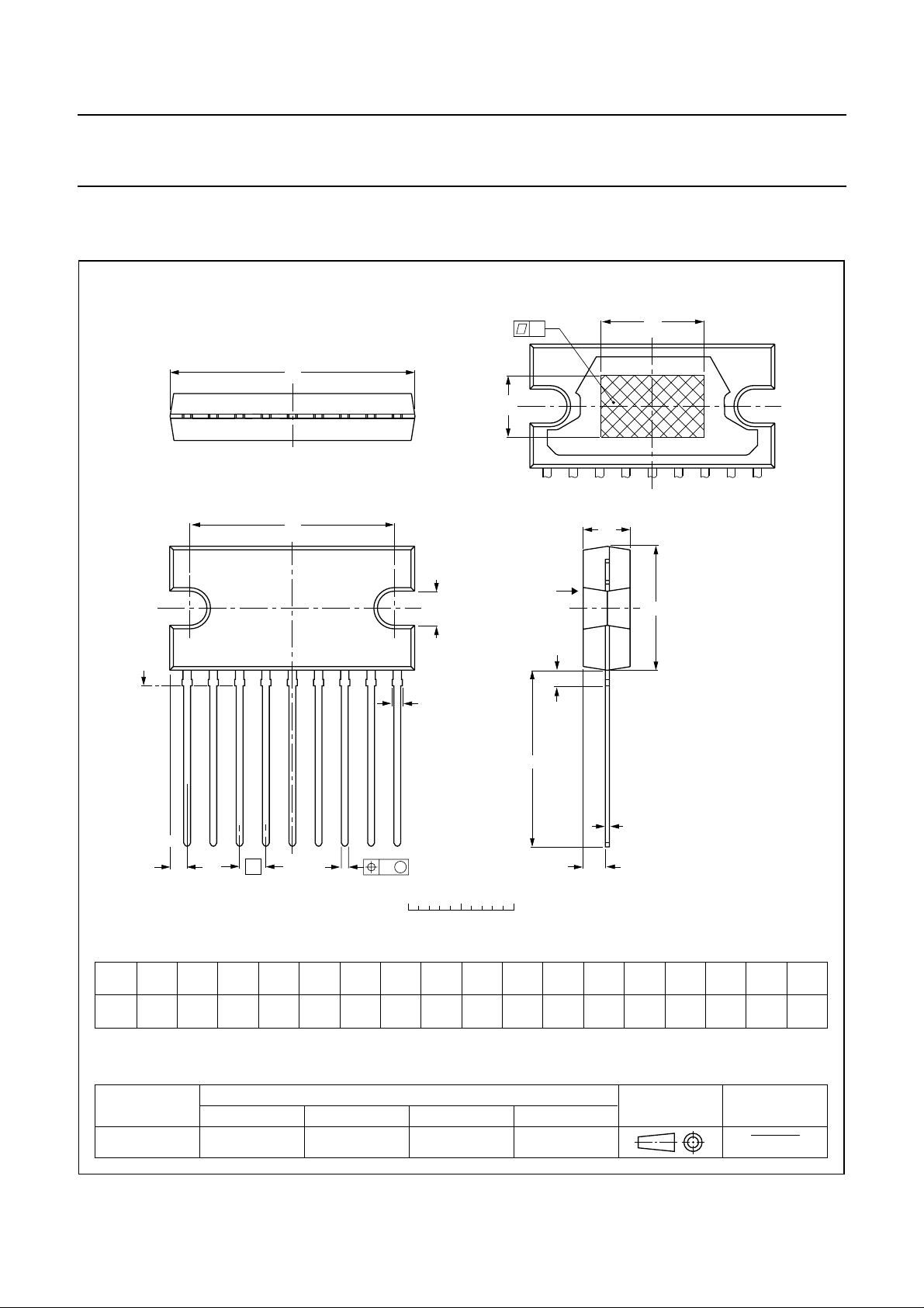
SIL9P: plastic single in-line power package; 9 leads
D
d
TDA1519C
SOT131-2
non-concave
x
E
h
view B: mounting base side
B
j
D
h
A
2
E
seating plane
b
19
Z
DIMENSIONS (mm are the original dimensions)
A
UNIT A
mm
Note
1. Plastic or metal protrusions of 0.25 mm maximum per side are not included.
1
max.
2.0
OUTLINE
VERSION
SOT131-2
4.6
4.4
e
b
b
cD
max.
1.1
p2
0.75
0.48
0.60
0.38
IEC JEDEC EIAJ
b
p
(1)
24.0
23.6
REFERENCES
w M
0 5 10 mm
scale
deD
h
20.0
10 2.54
19.6
E
12.2
11.8
A
1
L
c
Q
(1)
E
h
6
3.4
3.1
Lj
Q
17.2
2.1
16.5
1.8
EUROPEAN
PROJECTION
0.25w0.03
ISSUE DATE
95-03-11
99-12-17
(1)
Z
x
2.00
1.45
2001 Aug 24 13
Page 14
Philips Semiconductors Product specification
22 W BTL or 2 × 11 W
stereo power amplifier
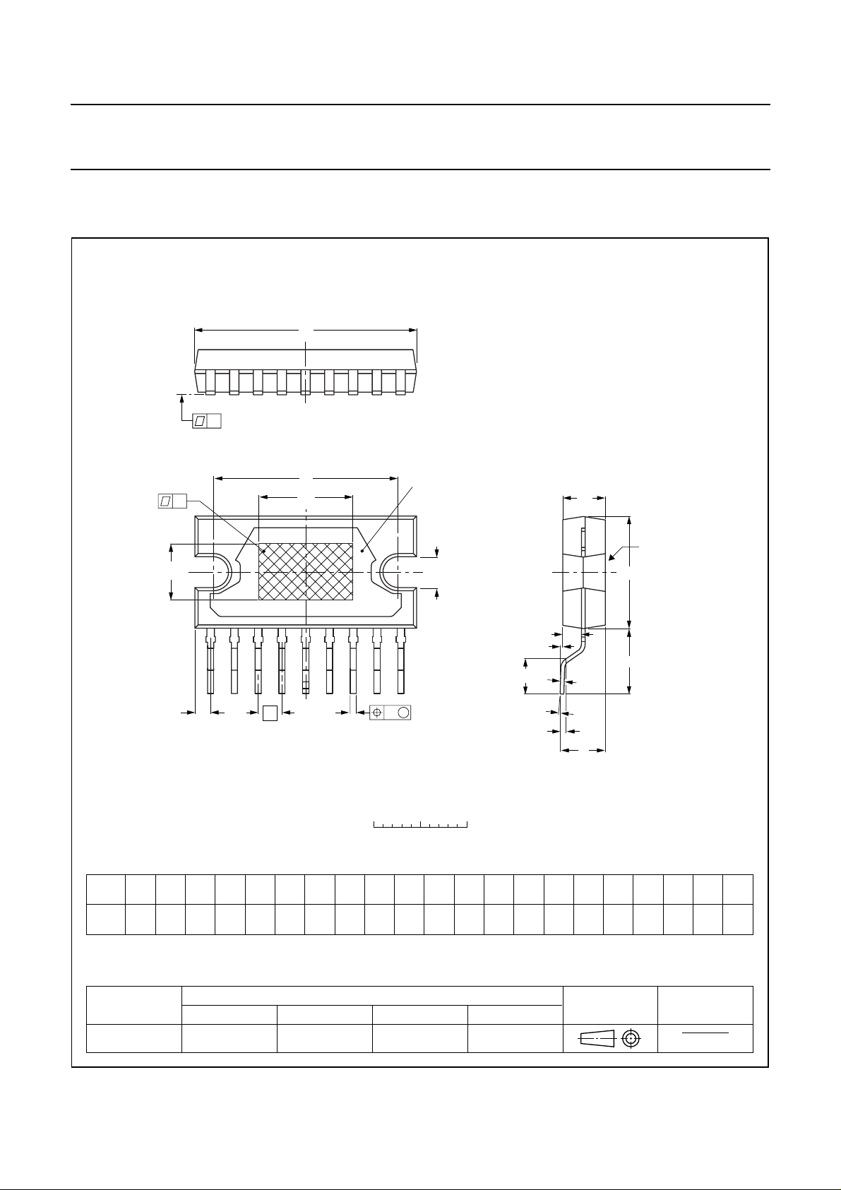
SMS9P: plastic surface mounted single in-line power package; 9 leads
D
y
non-concave
x
d
D
h
heatsink
TDA1519C
SOT354-1
A
2
E
h
91
w
M
0 5 10 mm
scale
(1)
E
h
12.2
10
11.8
0.75
0.60
e
0.48
0.38
b
p
(1)
deD
24.0
20.0
23.6
19.6
Z
DIMENSIONS (mm are the original dimensions)
UNIT A A1A2A3bpcD
4.9
0.35
mm
4.2
Note
1. Plastic or metal protrusions of 0.25 mm maximum per side are not included.
0.05
4.6
4.4
0.25
j
Q
A
1
L
p
c
θ
(A3)
A
E
h
6
2.54
j
3.4
3.1
L
L
7.4
6.6
Q
p
3.4
2.1
2.8
1.9
wxy θ
E
L
heatsink
0.030.25
0.15
Z
2.00
1.45
(1)
3°
0°
OUTLINE
VERSION
SOT354-1
IEC JEDEC EIAJ
REFERENCES
2001 Aug 24 14
EUROPEAN
PROJECTION
ISSUE DATE
98-10-08
99-12-17
Page 15
Philips Semiconductors Product specification
22 W BTL or 2 × 11 W
stereo power amplifier
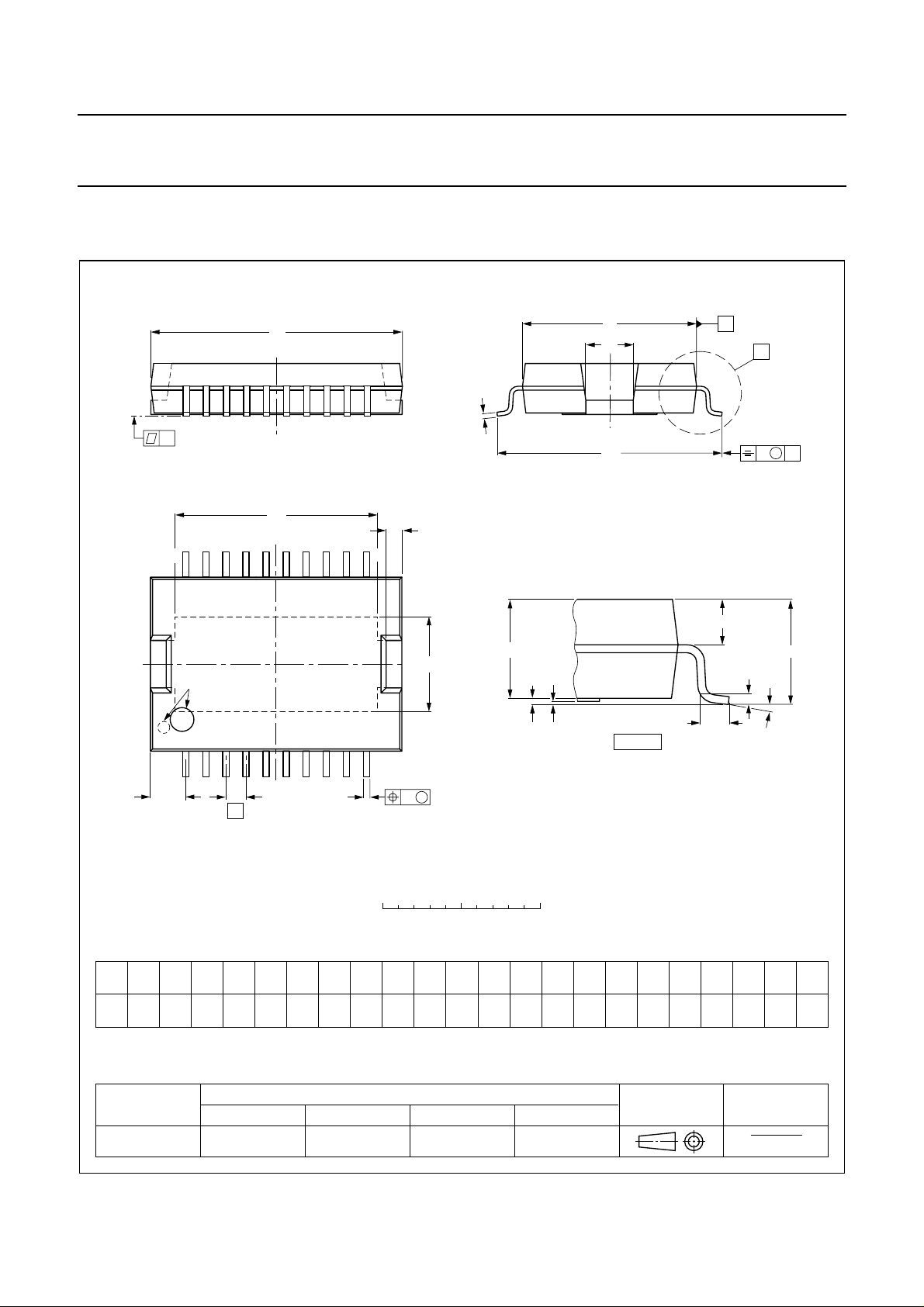
HSOP20: plastic, heatsink small outline package; 20 leads
D
y
D
1
20
11
D
2
TDA1519C
SOT397-1
E
E
2
c
H
E
A
X
v M
A
E
1
pin 1 index
1
Z
DIMENSIONS (mm are the original dimensions)
A
UNIT
mm
Note
1. Plastic or metal protrusions of 0.25 mm maximum per side are not included.
A
1
max.
0.3
3.6 0.35
0.1
A
3.3
3.0
e
A
0.1
0
4
bpc
0.53
0.40
0.32
0.23
A
2
3
10
w M
b
p
0 5 10 mm
scale
D
16.0
15.8
(1)
D
1
13.0
12.6
D
1.1
0.9
(1)
E
2
11.1
10.9
E
6.2
5.8
Q
A
2
A1A
4
detail X
H
L
Q
1.5
1.4
v
0.25w0.25
E
e
E
14.5
13.9
p
1.1
0.8
1
2
2.9
1.27
2.5
(A3)
L
p
0.1
A
θ
yZ
2.5
2.0
θ
8°
0°
OUTLINE
VERSION
SOT397-1
IEC JEDEC EIAJ
REFERENCES
2001 Aug 24 15
EUROPEAN
PROJECTION
ISSUE DATE
97-11-03
99-11-12
Page 16
Philips Semiconductors Product specification
22 W BTL or 2 × 11 W
stereo power amplifier
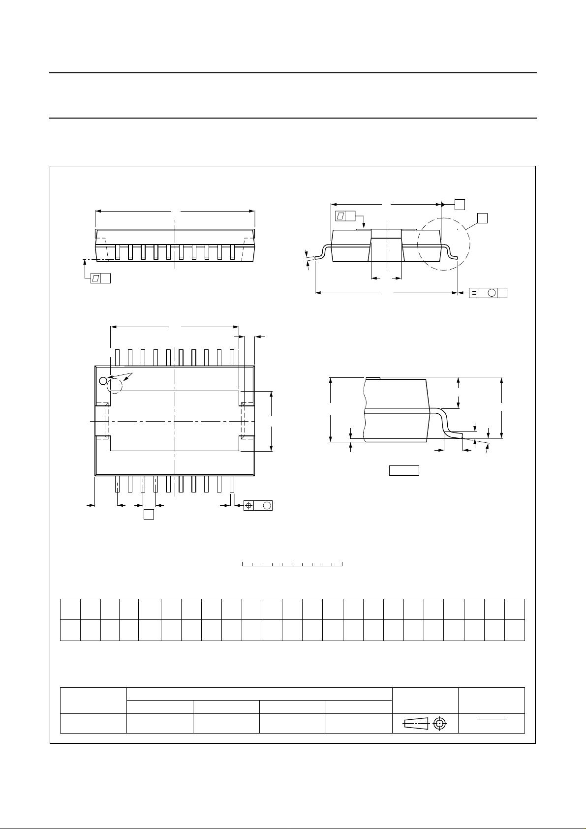
HSOP20: plastic, heatsink small outline package; 20 leads; low stand-off height
D
c
y
D
1
1
pin 1 index
10
D
2
x
E
E
2
H
E
TDA1519C
SOT418-2
A
X
v
M
A
E
1
20
Z
DIMENSIONS (mm are the original dimensions)
A
UNIT
mm
Notes
1. Limits per individual lead.
2. Plastic or metal protrusions of 0.25 mm maximum per side are not included.
A
2
max.
3.5
3.5 0.35
3.2
e
(1)
A
4
+0.12
−0.02
bpc
0.53
0.40
A
3
0.32
0.23
D
16.0
15.8
11
w
b
p
(2)
D
1
13.0
12.6
M
0 5 10 mm
scale
(2)
D
1.1
0.9
2
E
11.1
10.9
E
6.2
5.8
1
E
2.9
2.5
Q
A
2
A
4
detail X
H
L
Q
1.7
1.5
v
0.25w0.25
e
E
14.5
13.9
p
1.1
0.8
2
1.27
L
x
0.03
(A3)
p
0.07
A
θ
yZ
2.5
2.0
θ
8°
0°
OUTLINE
VERSION
SOT418-2
IEC JEDEC EIAJ
REFERENCES
2001 Aug 24 16
EUROPEAN
PROJECTION
ISSUE DATE
98-02-25
99-11-12
Page 17

Philips Semiconductors Product specification
22 W BTL or 2 × 11 W
stereo power amplifier
SOLDERING
Introduction
Thistextgives a very briefinsight toacomplex technology.
A more in-depth account of soldering ICs can be found in
our
“Data Handbook IC26; Integrated Circuit Packages”
(document order number 9398 652 90011).
There is no soldering method that is ideal for all IC
packages. Wave soldering is often preferred when
through-holeandsurfacemountcomponentsare mixed on
one printed-circuit board. Wave soldering can still be used
for certain surface mount ICs, but it is not suitable for fine
pitch SMDs. In these situations reflow soldering is
recommended.
Through-hole mount packages
SOLDERING BY DIPPING OR BY SOLDER WAVE
The maximum permissible temperature of the solder is
260 °C; solder at this temperature must not be in contact
with the joints for more than 5 seconds. The total contact
time of successive solder waves must not exceed
5 seconds.
The device may be mounted up to the seating plane, but
the temperature of the plastic body must not exceed the
specified maximum storage temperature (T
printed-circuit board has been pre-heated, forced cooling
may be necessary immediately after soldering to keep the
temperature within the permissible limit.
MANUAL SOLDERING
Apply the soldering iron (24 V or less) to the lead(s) of the
package, either below the seating plane or not more than
2 mm above it. If the temperature of the soldering iron bit
is less than 300 °C it may remain in contact for up to
10 seconds. If the bit temperature is between
300 and 400 °C, contact may be up to 5 seconds.
Surface mount packages
REFLOW SOLDERING
Reflow soldering requires solder paste (a suspension of
fine solder particles, flux and binding agent) to be applied
tothe printed-circuit board byscreen printing, stencilling or
pressure-syringe dispensing before package placement.
Several methods exist for reflowing; for example,
convection or convection/infrared heating in a conveyor
type oven. Throughput times (preheating, soldering and
cooling) vary between 100 and 200 seconds depending
on heating method.
stg(max)
). If the
TDA1519C
Typical reflow peak temperatures range from
215 to 250 °C. The top-surface temperature of the
packages should preferable be kept below 220 °C for
thick/large packages, and below 235 °C for small/thin
packages.
WAVE SOLDERING
Conventional single wave soldering is not recommended
forsurfacemount devices (SMDs) or printed-circuitboards
with a high component density, as solder bridging and
non-wetting can present major problems.
To overcome these problems the double-wave soldering
method was specifically developed.
If wave soldering is used the following conditions must be
observed for optimal results:
• Use a double-wave soldering method comprising a
turbulent wave with high upward pressure followed by a
smooth laminar wave.
• For packages with leads on two sides and a pitch (e):
– larger than or equal to 1.27 mm, the footprint
longitudinal axis is preferred to be parallel to the
transport direction of the printed-circuit board;
– smaller than 1.27 mm, the footprint longitudinal axis
must be parallel to the transport direction of the
printed-circuit board.
The footprint must incorporate solder thieves at the
downstream end.
• Forpackageswith leads on four sides,the footprintmust
be placed at a 45° angle to the transport direction of the
printed-circuit board. The footprint must incorporate
solder thieves downstream and at the side corners.
During placement andbefore soldering, the package must
be fixed with a droplet of adhesive. The adhesive can be
applied by screen printing, pin transfer or syringe
dispensing. The package can be soldered after the
adhesive is cured.
Typical dwell time is 4 seconds at 250 °C.
A mildly-activated flux will eliminate the need for removal
of corrosive residues in most applications.
MANUAL SOLDERING
Fix the component by first soldering two
diagonally-opposite end leads. Use a low voltage (24 V or
less) soldering iron applied to the flat part of the lead.
Contact time must be limited to 10 seconds at up to
300 °C. When using a dedicated tool, all other leads can
be soldered in one operation within 2 to 5 seconds
between 270 and 320 °C.
2001 Aug 24 17
Page 18

Philips Semiconductors Product specification
22 W BTL or 2 × 11 W
TDA1519C
stereo power amplifier
Suitability of IC packages for wave, reflow and dipping soldering methods
MOUNTING PACKAGE
Through-hole mount DBS, DIP, HDIP, SDIP, SIL suitable
Surface mount BGA, HBGA, LFBGA, SQFP, TFBGA not suitable suitable −
HBCC, HLQFP, HSQFP, HSOP, HTQFP,
HTSSOP, HVQFN, SMS
(4)
PLCC
LQFP, QFP, TQFP not recommended
SSOP, TSSOP, VSO not recommended
Notes
1. All surface mount (SMD) packages are moisture sensitive. Depending upon the moisture content, the maximum
temperature (with respect to time) and body size of the package, there is a risk that internal or external package
cracks may occur due to vaporization of the moisture in them (the so called popcorn effect). For details, refer to the
Drypack information in the
2. For SDIP packages, the longitudinal axis must be parallel to the transport direction of the printed-circuit board.
3. These packages are not suitable for wave soldering as a solder joint between the printed-circuit board and heatsink
(at bottom version) can not be achieved, and as solder may stick to the heatsink (on top version).
4. If wave soldering is considered, then the package must be placed at a 45° angle to the solder wave direction.
The package footprint must incorporate solder thieves downstream and at the side corners.
5. Wave soldering is only suitable for LQFP, QFP and TQFP packages with a pitch (e) equal to or larger than 0.8 mm;
it is definitely not suitable for packages with a pitch (e) equal to or smaller than 0.65 mm.
6. Wave soldering is only suitable for SSOP and TSSOP packages with a pitch (e)equal toor larger than 0.65 mm; it is
definitely not suitable for packages with a pitch (e) equal to or smaller than 0.5 mm.
, SO, SOJ suitable suitable −
“Data Handbook IC26; Integrated Circuit Packages; Section: Packing Methods”
not suitable
SOLDERING METHOD
WAVE REFLOW
(2)
(3)
− suitable
suitable −
(4)(5)
suitable −
(6)
suitable −
(1)
DIPPING
.
2001 Aug 24 18
Page 19

Philips Semiconductors Product specification
22 W BTL or 2 × 11 W
TDA1519C
stereo power amplifier
DATA SHEET STATUS
PRODUCT
DATA SHEET STATUS
Objective data Development This data sheet contains data from the objective specification for product
Preliminary data Qualification This data sheet contains data from the preliminary specification.
Product data Production This data sheet contains data from the product specification. Philips
Notes
1. Please consult the most recently issued data sheet before initiating or completing a design.
2. The product status of the device(s) described in this data sheet may have changed since this data sheet was
published. The latest information is available on the Internet at URL http://www.semiconductors.philips.com.
(1)
STATUS
(2)
development. Philips Semiconductors reserves the right to change the
specification in any manner without notice.
Supplementary data will be published at a later date. Philips
Semiconductors reserves the right to change the specification without
notice, in order to improve the design and supply the best possible
product.
Semiconductors reserves the right to make changes at any time in order
to improve the design, manufacturing and supply. Changes will be
communicated according to the Customer Product/Process Change
Notification (CPCN) procedure SNW-SQ-650A.
DEFINITIONS
DEFINITIONS
Short-form specification The data in a short-form
specification is extracted from a full data sheet with the
same type number and title. For detailed information see
the relevant data sheet or data handbook.
Limiting values definition Limiting values given are in
accordance with the Absolute Maximum Rating System
(IEC 60134). Stress above one or more of the limiting
values may cause permanent damage to the device.
These are stress ratings only and operation of the device
atthese or at any otherconditionsabove those given inthe
Characteristics sections of the specification is not implied.
Exposure to limiting values for extended periods may
affect device reliability.
Application information Applications that are
described herein for any of these products are for
illustrative purposes only. Philips Semiconductors make
norepresentationorwarranty that such applications will be
suitable for the specified use without further testing or
modification.
DISCLAIMERS
Life support applications These products are not
designed for use in life support appliances, devices, or
systems where malfunction of these products can
reasonably be expected to result inpersonal injury. Philips
Semiconductorscustomersusingor selling these products
for use in such applications do so at their own risk and
agree to fully indemnify Philips Semiconductors for any
damages resulting from such application.
Right to make changes Philips Semiconductors
reserves the right to make changes, without notice, in the
products, including circuits, standard cells, and/or
software, described or contained herein in order to
improve design and/or performance. Philips
Semiconductors assumes no responsibility or liability for
theuseof any of these products,conveys nolicence ortitle
under any patent, copyright, or mask work right to these
products,and makes no representationsorwarranties that
these products are free from patent, copyright, or mask
work right infringement, unless otherwise specified.
2001 Aug 24 19
Page 20

Philips Semiconductors – a w orldwide compan y
Contact information
For additional information please visit http://www.semiconductors.philips.com. Fax: +31 40 27 24825
For sales offices addresses send e-mail to: [email protected].
© Koninklijke Philips Electronics N.V. 2001
All rights are reserved. Reproduction in whole or in part is prohibited without the prior written consent of the copyright owner.
The information presented in this document does not form part of any quotation or contract, is believed to be accurate and reliable and may be changed
without notice. No liability will be accepted by the publisher for any consequence of its use. Publication thereof does not convey nor imply any license
under patent- or other industrial or intellectual property rights.
Printed in The Netherlands 753503/03/pp20 Date of release: 2001 Aug 24 Document order number: 9397750 08284
SCA73
 Loading...