

Page 1
Philips Semiconductors Product specification
Quadruple filter DAC TDA1314T
FEATURES
• High dynamic range to enable digital DSP (Digital Signal
Processor) volume control
APPLICATIONS
• Stand-alone quadruple low noise DAC
• Car radio DAC in conjunction with DSP.
• 18 bits data input format for each of the four channels
• Four times bit-serial oversampling filter
• 1st-order 4fas (audio sampling frequency) noise shaper
• Four very low noise DACs
• Only 1st-order analog post filtering required
• Smooth power-on of the DAC output currents
• Because of the automatic digital PLL divider range
setting the master clock is selectable in a wide 4f
as
integer range
GENERAL DESCRIPTION
The TDA1314T is a quadruple very low noise high
dynamic range DAC which is intended for use in motor
cars and is controlled by the car radio DSP. Each channel
incorporates an 8th-order IIR up-sampling filter from 1ASF
to 4ASF followed by a 1st-order noise shaper and DAC.
The DAC currents are converted to audio voltage signals
using operational amplifiers (one per channel).
• Insensitive to jitter on the I2S-bus signals with respect to
the DAC total harmonic distortion deterioration.
QUICK REFERENCE DATA
V
= 2.5 and 5 V; T
ref
= 25 °C; all voltages referenced to ground; unless otherwise specified.
amb
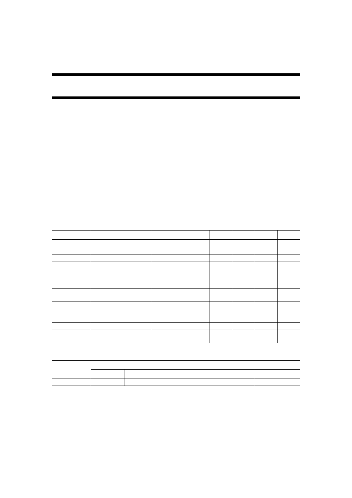
SYMBOL PARAMETER CONDITIONS MIN. TYP. MAX. UNIT
V
DDA
V
DDD
I
O(DAC)
V
O(DAC)
analog supply voltage 4.5 5.0 5.5 V
digital supply voltage 4.5 5.0 5.5 V
DAC output current (FS) R
DAC output voltage,
= 20.5 kΩ ±0.4 ±0.5 ±0.6 mA
ref
RL≥ 5 kΩ; Rfb= 3 kΩ 1.0 − 4.0 V
nominal DAC operational
amplifier output voltage
RES DAC resolution length of data input word − − 18 bits
(THD + N)/S total harmonic distortion
plus noise-to-signal ratio
DR dynamic range of DAC fi= 1 kHz;
fi= 1 kHz;
0 dB signal level
− −66 −56 dB
92 96 − dB
−60 dB signal level
DS digital silence no signal; A-weighted − −110 −100 dB
P
tot
T
amb
total power dissipation − 85 − mW
operating ambient
−40 +25 +85 °C
temperature
ORDERING INFORMATION
TYPE NUMBER
NAME DESCRIPTION VERSION
PACKAGE
TDA1314T SO28 plastic small outline package; 28 leads; body width 7.5 mm SOT136-1
August 1994 2
Page 2
Philips Semiconductors Product specification
handbook, full pagewidth
MBE001
20 20
5
20-bit
DATA WORD
LATCH
NOISE
SHAPER
15
15-bit
DATA WORD
LATCH
5
THERM.
DEC.
9
MSB
1 2 3 31 32
COARSE CURRENT SOURCES
I
ref
FINE
CURRENT
MATRIX
CURRENT
DIRECTION
SWITCH
I
out-f
I
out-c
DAC LATCH
I
out
DAC FL
4 f
UP-SAMPLE
FILTER
s
4 f
s
4 f
UP-SAMPLE
FILTER
s
4 f
UP-SAMPLE
FILTER
s
4 f
UP-SAMPLE
FILTER
s
NOISE
SHAPER
DAC
LATCH
DAC FR
NOISE
SHAPER
DAC
LATCH
DAC RL
NOISE
SHAPER
DAC
LATCH
DAC RR
181818
18
I S
INTERFACE
2
10
11
I
ORR
V
ORR
12
13
I
ORL
V
ORL
17
18
I
OFR
V
OFR
19
20
I
OFL
V
OFL
R
ref
V
ref
21
14
16 15
OGND
229876
POWER-UP
V
DDA
V
DDO
V
DDD
AGNDDGND
TEST
INTERFACE
test
signals
UP-SAMPLE
CLOCK GENERATOR
SYNTHESIZER
DIVIDED BY 45 . . . 128
5
3
4 ASF GENERATOR
FASF DAC
UPSAMPLE
CLOCKS
23
MCLK
SELINPH
WS
SCK
SDF
SDR
26425
24
AT/DT
TC
SCOUT1
SCOUT2
2
1
27
28
CMT
TDA1314T
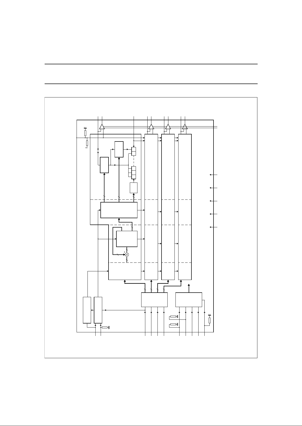
Fig.1 Block diagram.
Quadruple filter DAC TDA1314T
BLOCK DIAGRAM
August 1994 3
Page 3

Philips Semiconductors Product specification
Quadruple filter DAC TDA1314T
PINNING
SYMBOL PIN DESCRIPTION
TC 1 test control signal input (test/operational)
AT/DT 2 analog test/digital test select input
SELINPH 3 select in-phase 4fas mode/scan input signal 1 in test mode
SCK 4 serial clock input; I2S-bus
MCLK 5 master clock input; fi= N × 4fas (45 ≤ N ≤ 128)
DGND 6 digital ground
AGND 7 analog ground
V
DDD
V
DDA
I
ORR
V
ORR
I
ORL
V
ORL
R
ref
OGND 15 operational amplifier ground
V
DDO
I
OFR
V
OFR
I
OFL
V
OFL
V
ref
POWER-UP 22 analog mute input for all DACs
CMT 23 current mirror input test signal
SDR 24 serial data input for rear DACs (I2S-bus); scan input signal 2 in test mode
SDF 25 serial data input for front DACs (I2S-bus)
WS 26 word select input (I2S-bus)
SCOUT1 27 scan output signal 1 in test mode; 4fas signal
SCOUT2 28 scan output signal 2 in test mode; PLL lock indicator
8 digital supply voltage
9 analog supply voltage
10 DAC output current; rear right
11 DAC output voltage; rear right
12 DAC output current; rear left
13 DAC output voltage; rear left
14 resistor reference input for DACs current
16 operational amplifier supply
17 DAC output current; front right
18 DAC output voltage; front right
19 DAC output current; front left
20 DAC output voltage; front left
21 reference voltage input (1⁄2 operational amplifier supply voltage)
August 1994 4
Page 4

Philips Semiconductors Product specification
Fig.2 Pin configuration.
Quadruple filter DAC TDA1314T
FUNCTIONAL DESCRIPTION
I2S-bus interface
The word select input (pin 26) is connected to the word
select line of the I2S-bus interface. This interface has
a standard I2S-bus specification as described in the
Philips
“I2S-bus specification”
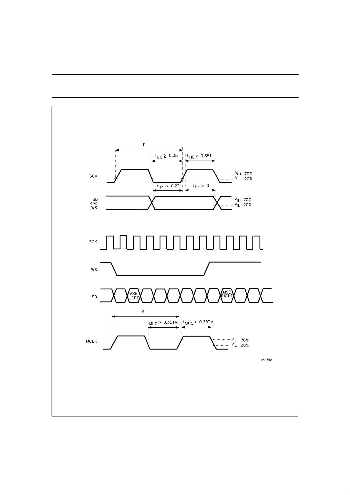
9398 332 10011). Figure 4 shows an excerpt of the Philips
I2S-bus specification interface report with respect to the
general timing and format of the I2S-bus. WS logic 0
means left channel word, logic 1 means right
channel word.
The serial clock input (pin 4) must be in accordance with
the I2S-bus specification, i.e. a continuous clock.
Serial data front (SDF, pin 25) and serial data rear (SDR,
pin 24) are the I2S-bus serial data lines to be processed in
the DACs for the loudspeakers of the car (see Fig.2, blocks
DACFL and DACFR for the front loudspeakers and blocks
DACRL and DACRR for the right loudspeakers). FL stands
for Front Left, FR for Front Right, RL for Rear Left and RR
for Rear Right. In order to utilize the capabilities of this IC
fully, the data word length should be 18 bits. Signals
derived from this block are 4 × 18-bit parallel data words
which are applied to the 4fs up-sample filters.
(ordering number
August 1994 5
4ASF generator
YNTHESIZER
S
SELINPH (pin 3) and WS (pin 26) are the data inputs for
this block which generates the FASFDAC, this being the
4fas signal (at 4 times the audio sample frequency), which
is used to latch the data words to the DACs and as a
reference to the clock generator block for the up-sample
filters. It consists of a digital PLL operating at the master
clock signal MCLK (pin 5). In normal mode (i.e. in the
event that the MCLK signal on pin 5 is a jitter free clock,
with a frequency of integer multiples between 45 and 128,
of 4 times the frequency of the WS signal) this block is able
to generate a jitter free FASFDAC signal for optimum
performance of the DAC. This mode is called the free
running mode.
If, in some applications, there is considerable jitter on the
MCLK while WS is more stable (less jitter), the
phase-locked mode should be selected. This mode is
normally not used and is not recommended.
Page 5

Philips Semiconductors Product specification
Quadruple filter DAC TDA1314T
UP-SAMPLE GENERATOR
This block generates the clocks for the up-sample
filters.The external pinning of the 4fas generator block is:
• MCLK (see Fig.4), which is a jitter free (maximum 30 ns
jitter) external clock at any multiple integer from
45 to 128 times 4fas (4 times the frequency of WS) of the
I2S-bus input, thus for a sample frequency of 38 kHz this
clock frequency will range from 6.840 MHz to
19.456 MHz in multiples of 152 kHz.
• The select in-phase (SELINPH) or free running mode of
the synthesizer 45 to 128. In the normal application the
free-running mode is used and this pin is not connected
(this pin is pulled down by an internal resistor). The
phase-locked mode can be selected by hard-wiring this
pin to V
(pin 8). However, this mode is
DDD
not recommended.
Test interface
This block controls the circuit in the test mode, which can
be either an analog or digital test mode. Test pins TC
(pin 1), AT/DT (pin 2), CMT (pin 23), SCOUT1 (pin 27)
and SCOUT2 (pin 28) are not connected in Fig.6.
Up-sample filter and noise shaper
The signal flow applied to the up-sample filter and noise
shaper blocks is the 4 × 18-bit parallel data words in two's
complement format from the I
2
S-bus interface at the audio
sampling frequency. The signal flow from these blocks is
the 4 × 15-bit parallel data words in two's complement
format at a frequency of 4fas. Each of the four digital filters
is a four times up-sampling filter. This up-sampling filter is
an elliptic filter of 8th order.
The filters produce an attenuation of 29 dB (min) for
signals outside the audio band. The noise shaper operates
at 4fas and reduces the word length from 22 bits to 15 bits
which is the word length of the DAC.
DAC input signals
The following signals are input to the DAC blocks FL, FR,
RL and RR:
• DATA WORD (bits 10 to 14). These 5 bits are used to
control, via a thermometer decoder, the current of the
32 coarse current sources of the analog DAC part. The
value of this data word determines the total coarse
current flowing to the DAC current output. The value of
the current of each coarse current source is determined
by the following:
; this is the current reference input at pin 14 and is at
R
ref
the same voltage level as V
. A resistor connected to
ref
OGND results in a current. This being the reference
current of the coarse current sources and subsequently
of the DAC in total.
• DATA WORD (bits 1 to 9). A current from one of the
coarse current sources is fed into a 512 transistor
matrix. The value of the DATA WORD (bits 1 to 9)
determines which part of one coarse current flows to the
DAC current output.
• DATA WORD (bit 15). This data word MSB controls the
direction of the flow of the DAC output current by
switching the current direction switch.
• V
. Voltage reference pin internally connected to a
ref
resistor divider to obtain half of the power supply
voltage. This voltage is buffered and used as reference
voltage input for the operational amplifiers and as a
reference voltage in the DAC.
• POWER-UP. The analog signal on this pin controls the
current biasing circuit of the DACs. This pin is connected
internally via a high value resistor to V
. Together with
DDA
an external capacitor a soft switch-on of the DAC output
currents is obtained. This pin can also be used as the
analog mute input for all DAC output currents by pulling
it to ground.
August 1994 6
Page 6
Philips Semiconductors Product specification
Fig.3 I2S-bus timing and format.
Quadruple filter DAC TDA1314T
August 1994 7
Page 7
Philips Semiconductors Product specification
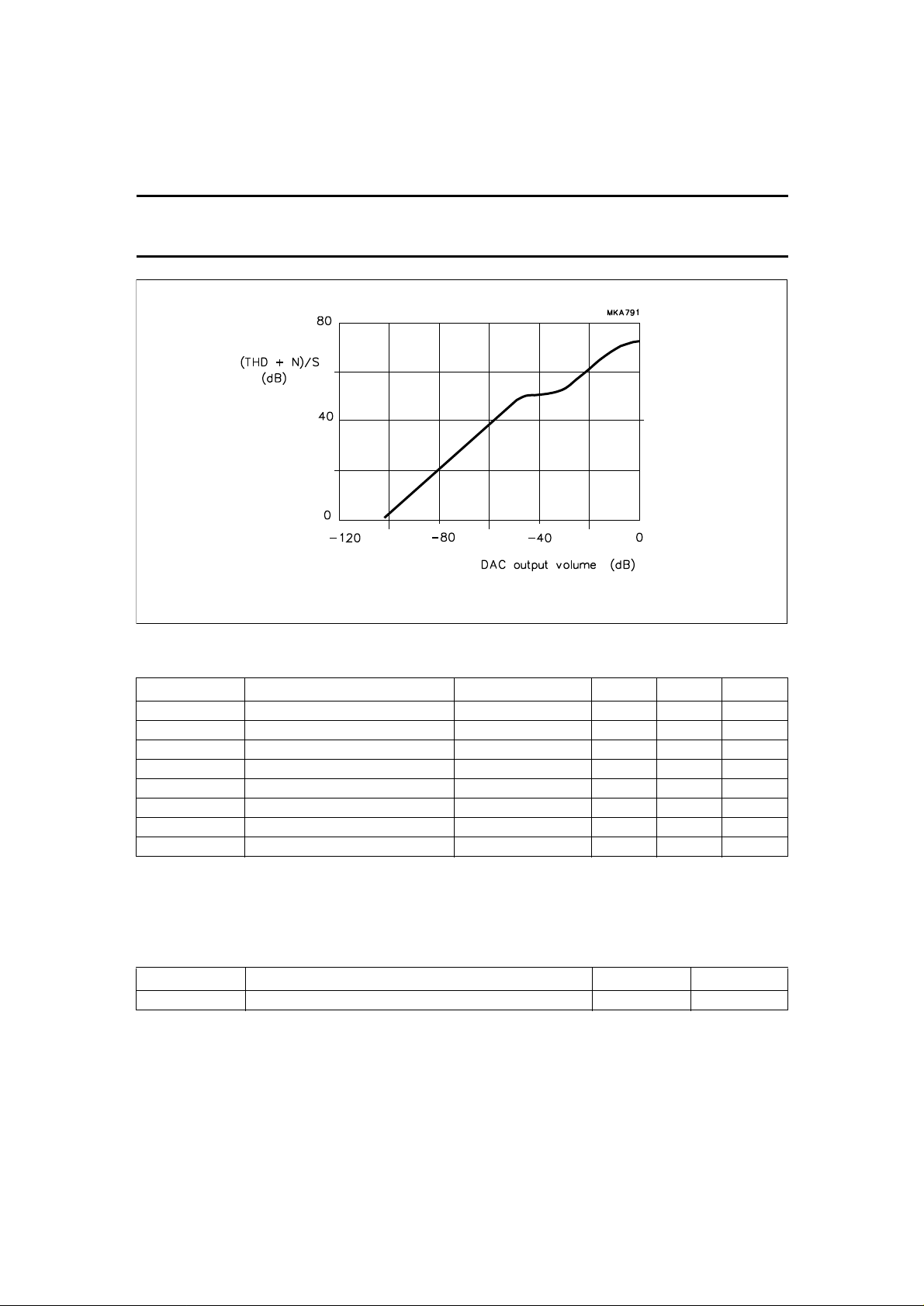
Fig.4 Total harmonic distortion plus noise-to-signal ratio as a function of output volume.
Quadruple filter DAC TDA1314T
LIMITING VALUES
In accordance with the Absolute Maximum Rating System (IEC 134).
SYMBOL PARAMETER CONDITIONS MIN. MAX. UNIT
V
V
V
V
T
T
T
V
DDD
DDA
DDO
n
xtal
stg
amb
es
digital supply voltage note 1 0 6.0 V
analog supply voltage note 1 0 6.0 V
operational amplifier supply voltage note 1 0 6.0 V
voltage on any other pin 0 V
DD
crystal temperature − +150 °C
storage temperature −55 +150 °C
operating ambient temperature −40 +85 °C
electrostatic handling note 2 −2000 +2000 V
Notes
1. All voltages (pins 6, 7 and 15) referenced to ground.
2. Equivalent to discharging a 100 pF capacitor through a 1.5 kΩ series resistor.
THERMAL CHARACTERISTICS
SYMBOL PARAMETER VALUE UNIT
R
th j-a
thermal resistance from junction to ambient in free air 76 K/W
V
August 1994 8
Page 8
Philips Semiconductors Product specification
Quadruple filter DAC TDA1314T
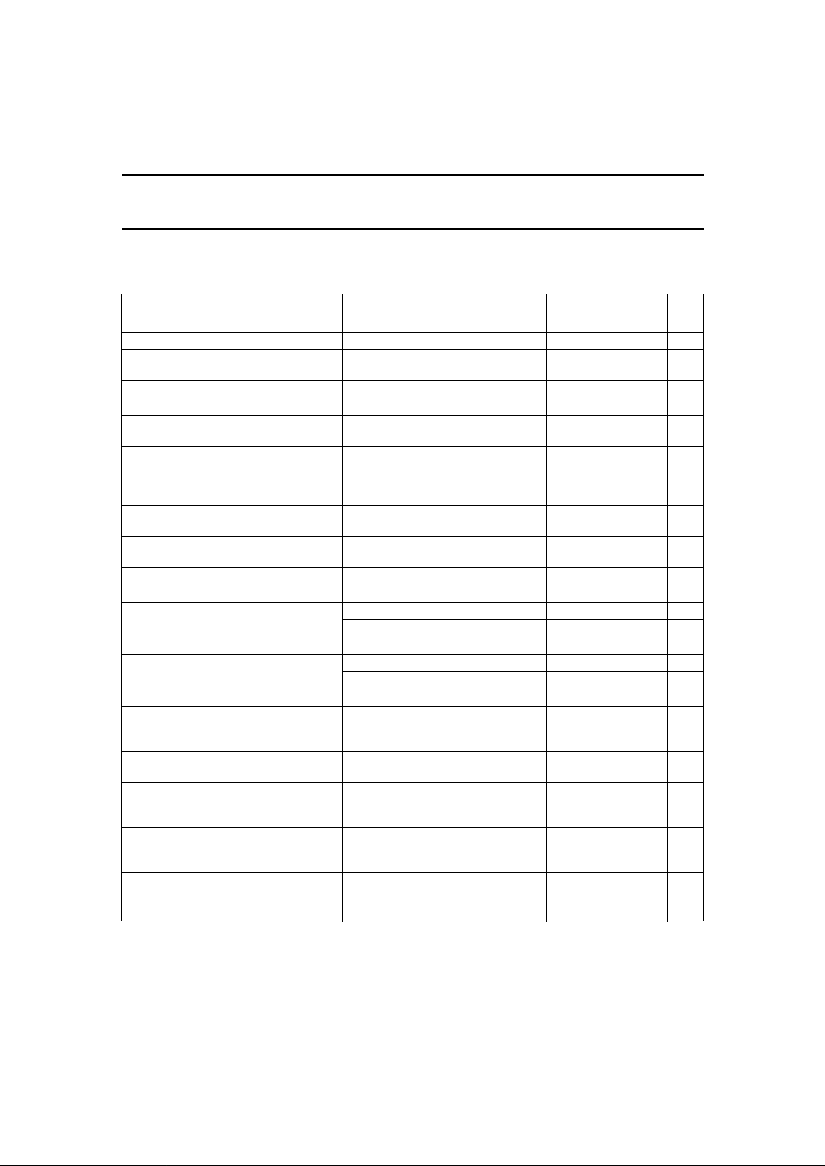
DC CHARACTERISTICS
VDD= 4.5 to 5.5 V; V
circuit of Fig.6; T
SYMBOL PARAMETER CONDITIONS MIN. TYP. MAX. UNIT
V
V
V
DDD
DDA
DDO
digital supply voltage 4.5 5.0 5.5 V
analog supply voltage 4.75 5.0 5.25 V
operational amplifier supply
voltage
I
DDD
I
DDA
I
DDO
digital supply current MCLK = 6.84 MHz − 10 17 mA
analog supply current at digital silence − 5 8 mA
operational amplifiers supply
current
P
tot
V
IH
total power dissipation MCLK = 6.84 MHz;
HIGH level input voltage
pins 1 to 5 and 23 to 26
V
IL
LOW level input voltage
pins 1 to 5 and 23 to 26
V
OH
HIGH level output voltage
pins 27 and 28
V
OL
LOW level output voltage
pins 27 and 28
V
ref
Z
I
V
I
I
ODAC(max)
reference input voltage with respect to OGND 0.45V
input impedance at pin 21 with respect to V
input voltage pin 14 with respect to OGND 0.43V
maximum output current
from DACs pins 10, 12, 17
and 19
V
O(os)
DC offset voltage at pins 10,
12, 17 and 19
V
OH(O)
HIGH level output voltage of
operational amplifiers at
pins 11, 13, 18 and 20
V
OL(O)
LOW level output voltage of
operational amplifiers at
pins 11, 13, 18 and 20
R
pu
R
pd
internal resistance at pin 22 with respect to V
internal resistance at
pins 1 to 3 and 23
Note
1. RL is the AC impedance of the external circuitry connected to the audio outputs in the application diagram of Fig.6.
= V
DDA
= 25 °C; unless otherwise specified.
amb
= 4.75 to 5.25 V; all voltage referenced to ground (pins 6, 7 and 15); measured in test
DDO
no operational amplifier
load resistor
at digital silence;
no operational amplifier
load resistor
V
V
V
V
with respect to OGND 15 20 30 kΩ
R
with respect to V
note 1; RL> 5 kΩ;
Rfb= 3 kΩ;
maximum signal
note 1; RL> 5 kΩ;
Rfb= 3 kΩ;
maximum signal
Vi= V
DGND
4.75 5.0 5.25 V
− 2 4 mA
− 85 145 mW
0.7V
− − 0.2V
= 4.5 V; IO= −4 mA 4.1 − − V
DDD
= 5.5 V; IO= −4.5 mA 5.1 − − V
DDD
= 4.5 V; IO= 4 mA − − 0.4 V
DDD
= 5.5 V; IO= 4.5 mA − − 0.4 V
DDD
15 20 30 kΩ
= 5 V 400 500 600 µA
− 5 − mV
V
DDO
= 20.5 kΩ; V
ref
DDO
DDO
ref
− − V
DDD
0.5V
DDO
DDO
− 1.3 V
0.5V
DDO
DDO
DDO
− 1 V
DDD
0.55V
0.57V
DDO
0.45 1.0 1.3 V
110 160 240 kΩ
27 − 80 kΩ
; with respect to
DDD
DDO
DDO
DDO
− 0.45 V
V
V
V
August 1994 9
Page 9
Philips Semiconductors Product specification
Quadruple filter DAC TDA1314T
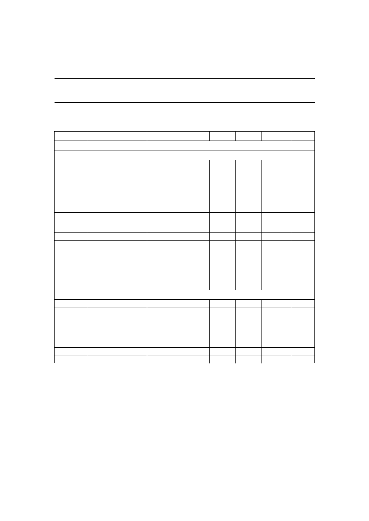
AC CHARACTERISTICS
V
= V
= V
DDD
DDA
DDO
= 5 V; T
Fig.5; unless otherwise specified.
SYMBOL PARAMETER CONDITIONS MIN. TYP. MAX. UNIT
ANALOG
S
DAC
SVRR supply voltage ripple
rejection pins 9 and 16
∆I
O(DAC)
maximum deviation of
output level of the 4 DAC
output currents with
respect to the average of
the 4 outputs
α
DAC
crosstalk between the
4 DAC current outputs
RES DAC resolution − − 18 bits
(THD + N)/S total harmonic distortion
plus noise-to-signal ratio
DR dynamic range fi= 1 kHz; −60 dB signal;
DS digital silence fi= 20 Hz to 17 kHz;
Operational amplifiers
G
v
open loop voltage gain − 85 − dB
PSRR power supply ripple
rejection
(THD + N)/S total harmonic distortion
plus noise as a function
of the operational
amplifiers signal
f
ug
Z
o
unity gain frequency open loop − 4.5 − MHz
output impedance RL> 5 kΩ − 1.5 150 Ω
= 25 °C; all voltages referenced to ground (pins 6, 7 and 15) measured in test circuit of
amb
f
= 1 kHz;
ripple
V
= 100 mV (peak);
ripple
C
= 22 µF
Vref
30 46 − dB
maximum volume − − 0.38 dB
2 outputs at digital
− −90 −60 dB
silence; 2 outputs at
maximum volume
fi= 1 kHz; 0 dB signal − −66 −56 dB
fi= 1 kHz; −60 dB signal;
− −36 −32 dB
A-weighted
92 96 − dB
A-weighted
− −110 −100 dB
A-weighted
f
= 3 kHz;
ripple
V
= 100 mV (peak)
ripple
RL> 5 kΩ (AC);
− 90 − dB
− −82 − dB
Rfb= 3 kΩ;
VO= 0.28 V (p-p);
fi= 1 kHz; A-weighted
August 1994 10
Page 10
Philips Semiconductors Product specification
--
=
--
=
--
=
--
=
--
=
--
=
Quadruple filter DAC TDA1314T
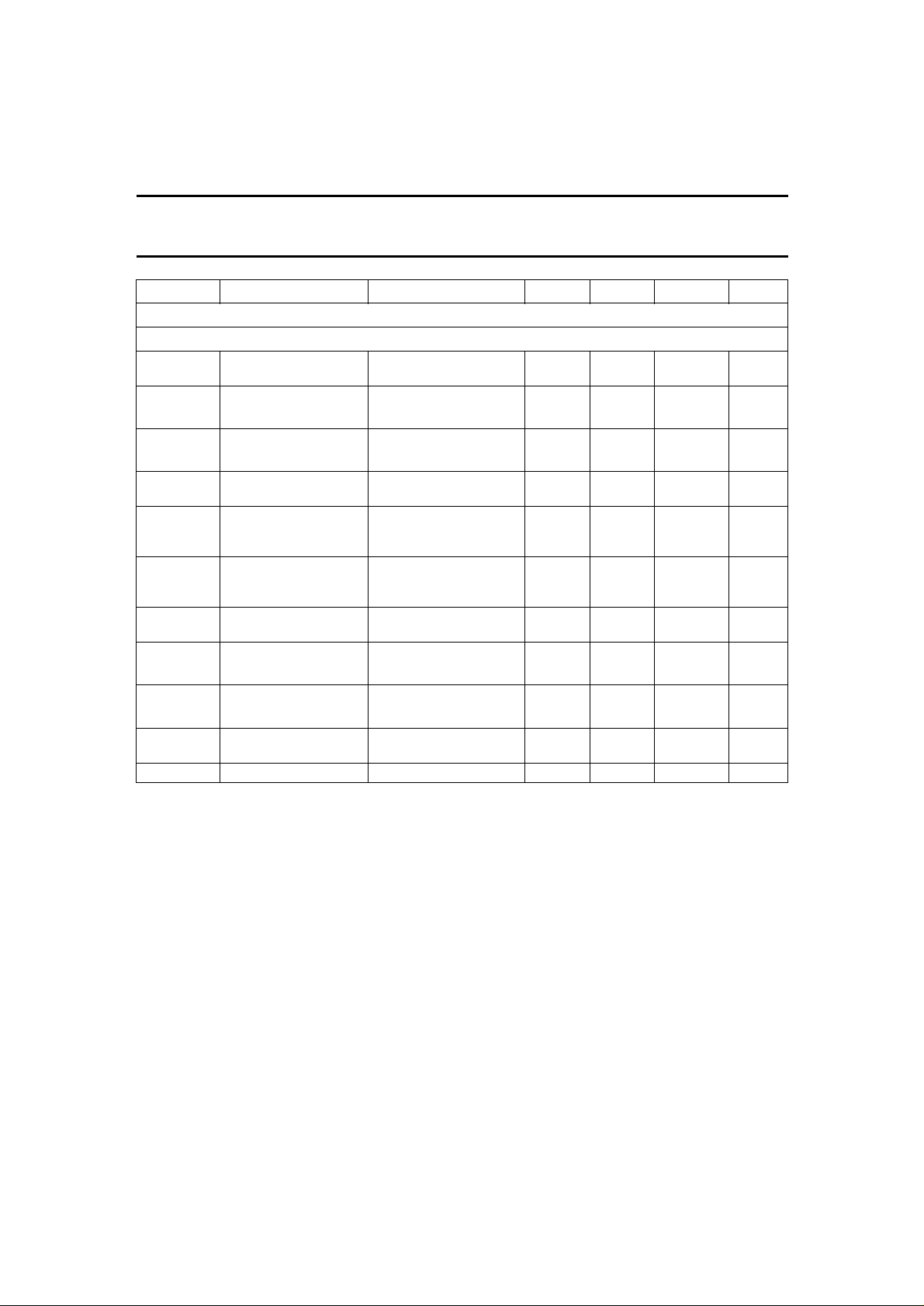
SYMBOL PARAMETER CONDITIONS MIN. TYP. MAX. UNIT
DIGITAL
I2S-BUS, UP-SAMPLING FILTER AND NOISE SHAPER
f
SCK
t
LC
t
HC
f
WS
t
sr
t
hr
f
MCLK
t
MLC
t
MHC
PR pass band ripple of
α
SB
serial clock input
ASF = 38 kHz 1.368 − 19.456 MHz
frequency
serial clock LOW time
serial clock HIGH time
word select input
at 20% V
at 70% V
DDD
DDD
;
T
--------f
SCK
;
T
--------f
SCK
0.35T − − µs
1
0.35T − − µs
1
38 44.1 48 kHz
frequency
set-up time from SDF,
SDR and WS to HIGH
going edge of SCK
hold time from SDF , SDR
and WS to HIGH going
edge of SCK
master clock input
frequency
master clock LOW time 0.35TM − − µs
master clock HIGH time 0.35TM − − µs
1
T
--------f
SCK
1
T
--------f
SCK
N × 4 × fWS;
where N = integer
--------f
SCK
--------f
SCK
1
1
TM
TM
with sample-and-hold
digital filter
from DAC
0.2T − − µs
0 − − µs
45 × 4fWS64 × 4fWS128 × 4fWSkHz
− 0.46 − dB
stop band attenuation fi> 22 kHz; no post filter 29 − − dB
August 1994 11
Page 11
Philips Semiconductors Product specification
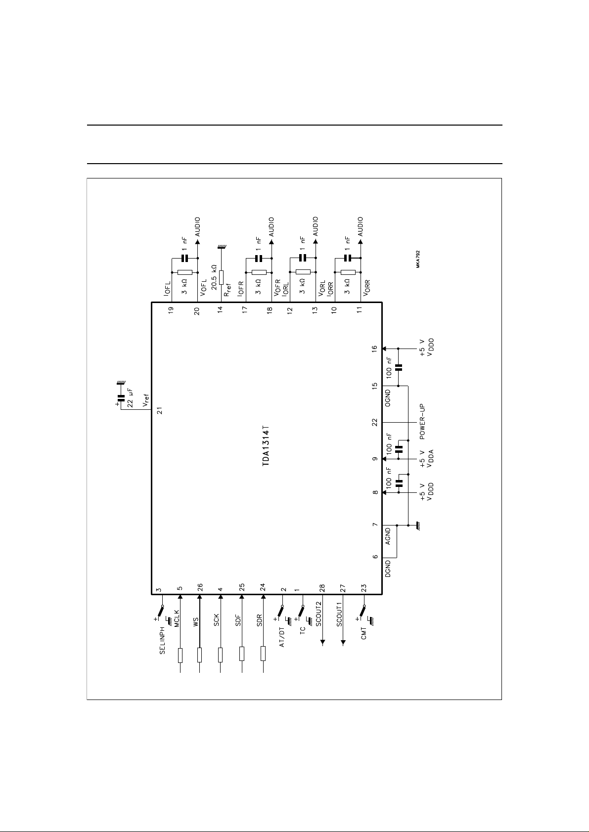
Fig.5 Test circuit.
Quadruple filter DAC TDA1314T
August 1994 12
Page 12

Philips Semiconductors Product specification
Quadruple filter DAC TDA1314T
APPLICATION INFORMATION
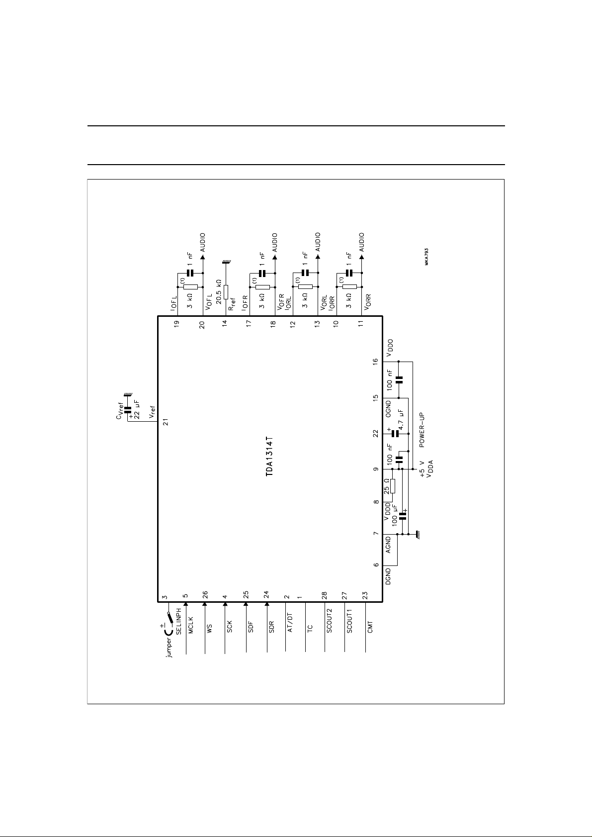
The application diagram is illustrated in Fig.6.
All pins used for testing (pins 1, 2, 23, 27 and 28 need not
to be connected due to internal resistors being connected
to ground or being used as test outputs. In the normal
free-running mode it is also not required to connect pin 3.
Jitter on the clock edges of MCLK must be as low as
possible so as not to deteriorate the DAC THD
performance. The jitter time must not be greater than
30 ns.
V
is the voltage reference pin with an internal resistor
ref
divider. A capacitor of 22 µF is used to get the specified
power ripple rejection ratio.
The output operational amplifiers are current-to-voltage
converters by means of the 3 kW resistors connected
between the DAC current outputs (pins 10, 12, 17 and 19)
and the voltage outputs (pins 11, 13, 18 and 20)
respectively. The voltage on the DAC current outputs is
equal to the operational amplifiers virtual ground at V
in
ref
the event that the operational amplifier is used according
to the application diagram of Fig.6.
Care should be taken, in order to reduce the
electromagnetic compatibility (EMC) that the bandwidth of
the digital signals being applied to pins MCLK, WS, SCK,
SDF and SDR is not larger than necessary. This can be
achieved by controlling the slew rate of the digital source
outputs or connecting a series resistor close to the digital
source output of the driving circuits.
The resistor connected between R
is the current reference of the DACs. The voltage on R
equal to V
.
ref
On the printed-circuit board V
(pin 14) and ground
ref
(pin 7) is also the
SSA
ref
substrate and has the most negative voltage of the IC, a
large as possible ground plane is therefore recommended.
The connection between V
short as possible. Pins V
must have capacitors connected to the V
closest to the chip. Pin V
, V
SSA
DDO
DDD
and V
SSD
and V
DDA
(pin 8) is fed via a small series
must be as
SSO
(pins 9 and 16)
ground plane
SSA
resistor (25 Ω). This resistor must be connected as close
as possible to pin 8.
The POWER-UP (pin 22) is connected via an electrolytic
capacitor to ground. This results in a smooth rising of the
DAC output currents at power-on. If this is not required
then this capacitor can be omitted.
Suppression of the higher harmonics by the up-sample
filter should be sufficient to protect the amplifiers and the
tweeter loudspeakers from excessive HF noise. The band
around 4fs cannot be attenuated by the 4ASF filter and is
only attenuated by the sample-and-hold effect of the DAC.
At frequencies above 100 kHz, additional attenuation
achieved by the 1st order post filter, which is built around
the buffer operational amplifiers. In total a 2nd order level
of filtering can be found above 100 kHz. In terms of power
the audio out-of-band power is approximately 15 × 10−4 of
the audio in-band power.
is
August 1994 13
Page 13
Philips Semiconductors Product specification
Fig.6 Application diagram.
Quadruple filter DAC TDA1314T
August 1994 14
Page 14
Philips Semiconductors Product specification
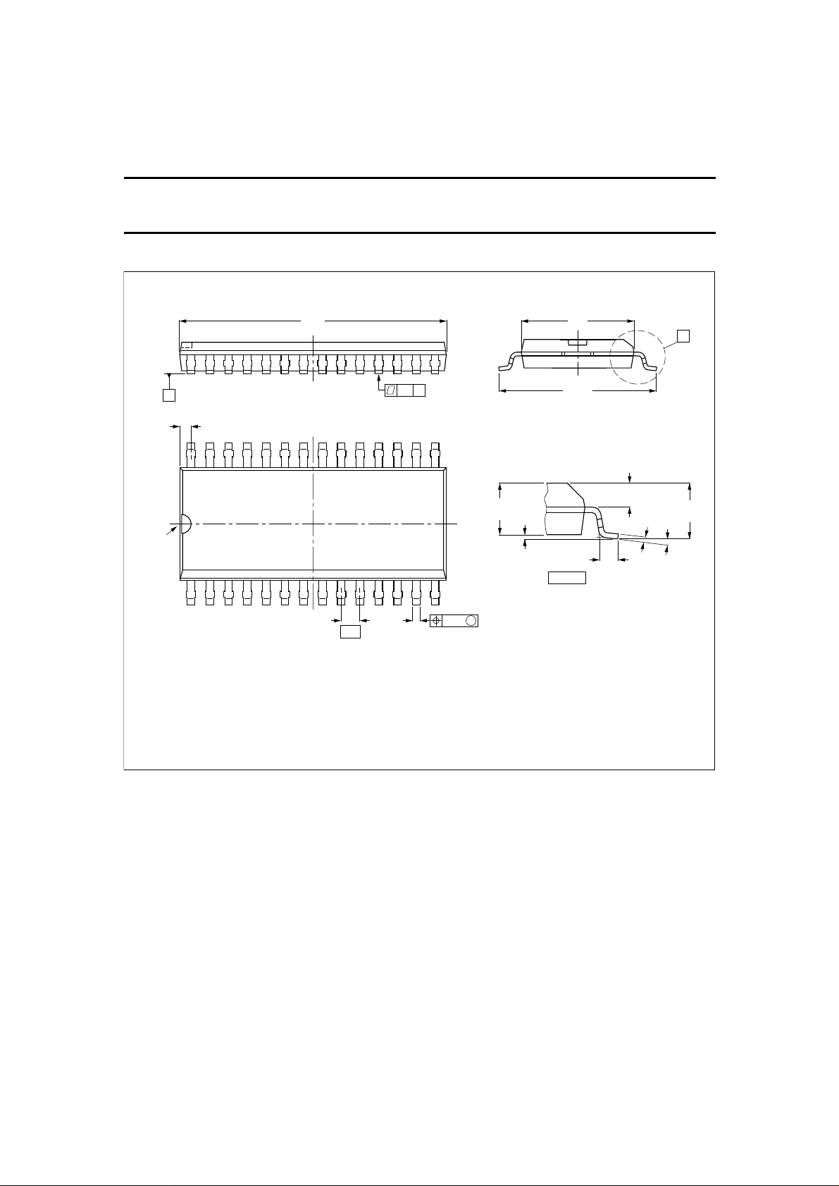
Fig.7 Plastic small outline package; 28 leads; body width 7.5 mm (SO28; SOT136-1).
Dimensions in mm.
handbook, full pagewidth
7.6
7.4
10.65
10.00
A
MBC236 - 1
0.3
0.1
2.45
2.25
1.1
0.5
0.32
0.23
1.1
1.0
0 to 8
o
2.65
2.35
detail A
S
18.1
17.7
0.1 S
1 14
1528
pin 1
index
0.9
0.4
(4x)
0.25 M
(28x)
0.49
0.36
1.27
Quadruple filter DAC TDA1314T
PACKAGE OUTLINE
August 1994 15
Page 15
Philips Semiconductors Product specification
Quadruple filter DAC TDA1314T
SOLDERING INFORMATION
Plastic small-outline packages
B
Y WAVE
During placement and before soldering, the component
must be fixed with a droplet of adhesive. After curing the
adhesive, the component can be soldered. The adhesive
can be applied by screen printing, pin transfer or syringe
dispensing.
Maximum permissible solder temperature is 260 °C, and
maximum duration of package immersion in solder bath is
10 s, if allowed to cool to less than 150 °C within 6 s.
Typical dwell time is 4 s at 250 °C.
A modified wave soldering technique is recommended
using two solder waves (dual-wave), in which a turbulent
wave with high upward pressure is followed by a smooth
laminar wave. Using a mildly-activated flux eliminates the
need for removal of corrosive residues in most
applications.
BY SOLDER PASTE REFLOW
Reflow soldering requires the solder paste (a suspension
of fine solder particles, flux and binding agent) to be
applied to the substrate by screen printing, stencilling or
pressure-syringe dispensing before device placement.
DEFINITIONS
Several techniques exist for reflowing; for example,
thermal conduction by heated belt, infrared, and
vapour-phase reflow. Dwell times vary between 50 and
300 s according to method. Typical reflow temperatures
range from 215 to 250 °C.
Preheating is necessary to dry the paste and evaporate
the binding agent. Preheating duration: 45 min at 45 °C.
EPAIRING SOLDERED JOINTS (BY HAND-HELD SOLDERING
R
IRON OR PULSE
-HEATED SOLDER TOOL)
Fix the component by first soldering two, diagonally
opposite, end pins. Apply the heating tool to the flat part of
the pin only. Contact time must be limited to 10 s at up to
300 °C. When using proper tools, all other pins can be
soldered in one operation within 2 to 5 s at between 270
and 320 °C. (Pulse-heated soldering is not recommended
for SO packages.)
For pulse-heated solder tool (resistance) soldering of VSO
packages, solder is applied to the substrate by dipping or
by an extra thick tin/lead plating before package
placement.
Data sheet status
Objective specification This data sheet contains target or goal specifications for product development.
Preliminary specification This data sheet contains preliminary data; supplementary data may be published later.
Product specification This data sheet contains final product specifications.
Limiting values
Limiting values given are in accordance with the Absolute Maximum Rating System (IEC 134). Stress above one or
more of the limiting values may cause permanent damage to the device. These are stress ratings only and operation
of the device at these or at any other conditions above those given in the Characteristics sections of the specification
is not implied. Exposure to limiting values for extended periods may affect device reliability.
Application information
Where application information is given, it is advisory and does not form part of the specification.
LIFE SUPPORT APPLICATIONS
These products are not designed for use in life support appliances, devices, or systems where malfunction of these
products can reasonably be expected to result in personal injury. Philips customers using or selling these products for
use in such applications do so at their own risk and agree to fully indemnify Philips for any damages resulting from such
improper use or sale.
August 1994 16
 Loading...