

Page 1

INTEGRATED CIRCUITS
DATA SH EET
TDA10085
Single Chip DVB-S/DSS Channel
Receiver
Preliminary specification
File under Integrated Circuits, IC02
2000 March 16
Page 2

Philips Semiconductors Preliminary specification
Single Chip DVB-S/DSS Channel Receiver TDA10085
FEATURES
• DSS and DVB-S compliant single chip demodulator & forward error correction.
• Dual 6-bit ADC on chip.
• New PLL which allows the use of a low-cost Xtal (typically 4 Mhz).
• DiSEqC 1.X from 1 to 8 bytes long sequences with modulated/unmodulated output.
• DSS dish control
• Digital Cancellation of A/D offset.
• Simultaneous Parallel and Serial Output interface.
• Variable rate BPSK/QPSK coherent demodulator.
• Modulation rate from 1 to 45MBaud.
• Automatic Gain Control output.
• Digital symbol timing recovery : Acquisition range up to ±
• Digital carrier recovery : Acquisition range up to 5Mhz
• Half Nyquist filters ( roll-off = 0.35 for DVB and 0.2 for DSS).
• Interpolating and anti-aliasing filters to handle variable symbol rate.
• Channel quality estimation.
• Spectral inversion ambiguity resolution.
• Viterbi decoder :
Supported rates : from 1/2 to 8/9.
Constraint length K = 7
with G1 = 171
Viterbi Output BER measurement.
Automatic code rate search within 1/2, 2/3 and 6/7 in DSS mode.
Automatic code rate search within 1/2, 2/3, 3/4, 5/6 and 7/8 in DVB-S mode.
• Convolutional deinterleaver and Reed Solomon decoder according to DVB and DSS specifications.
• Automatic Frame Synchronization.
• Selectable DVB-S descrambling.
2
C bus interface.
• I
• 64-pin TQFP package.
• CMOS technology (0.2 µ
G2 = 133
8
8
m 1.8V/3.3V).
960ppm
APPLICATIONS
• DVB-S receivers (ETS 300-421).
• DSS receivers.
DESCRIPTION
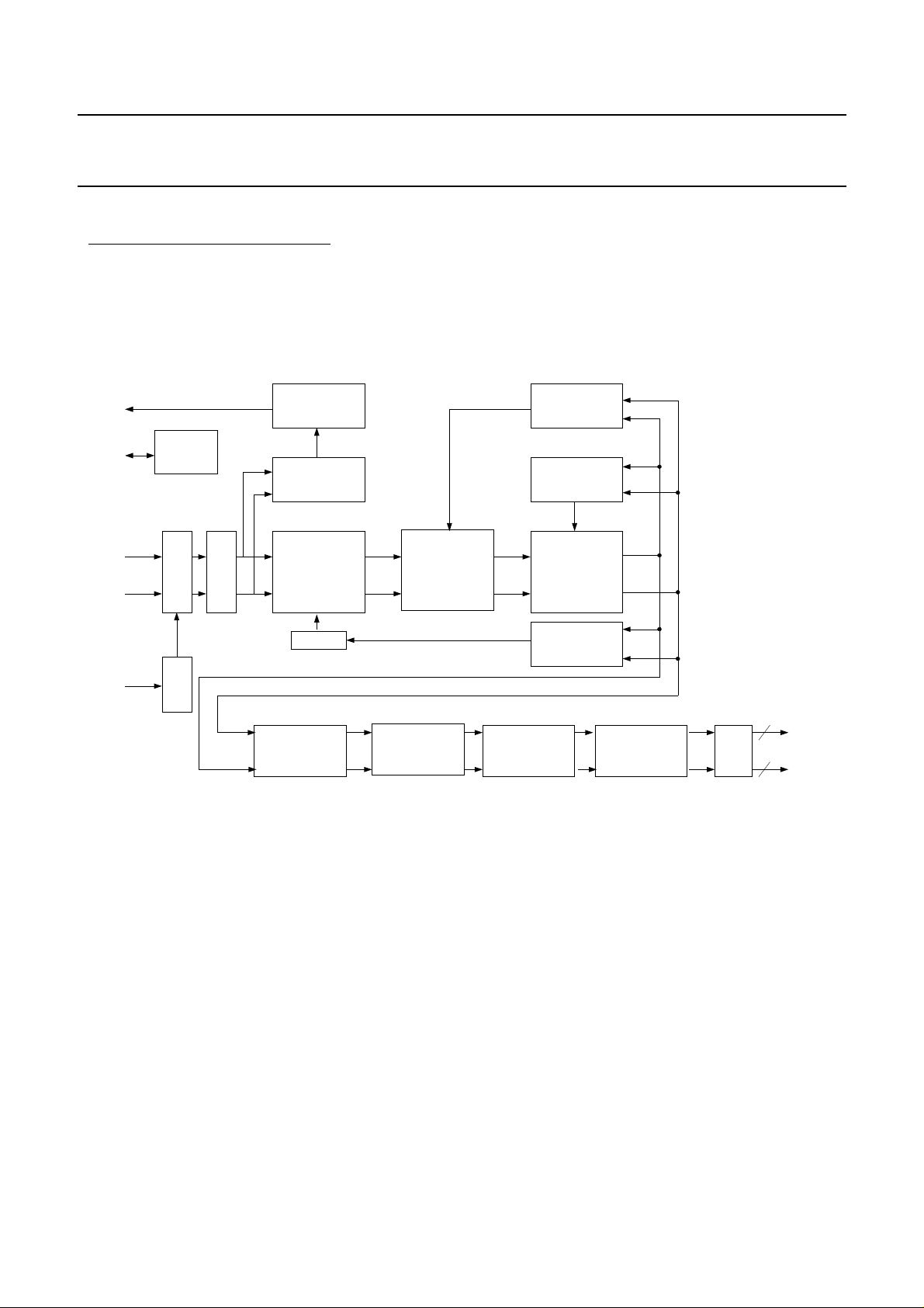
The TDA10085 is a single-chip channel receiver for satellite television reception which matches both DSS and
DVB-S standards. The device contains a dual 6-bit flash analog to digital converter, variable rate BPSK/Q PSK
coherent demodulator and Forward Error Correction functions. The ADCs directly interface with I and Q analog
baseband signals. After A to D conversion, the TDA10085 implements a bank of cascadable filters as well as
antialias and half-Nyquist filters. Analog AGC signal is generated by an amplitude estimation function. The
TDA10085 performs clock recovery at twice the Baud rate and achieves coherent demodulation without any
feedback to the local oscillator. Forward Error Correction is built around two error correcting codes : a ReedSolomon (outer code), and a Viterbi decoder (inner code). The Reed-Solomon decoder corrects up to 8 erroneous
bytes among the N (204) bytes of one data packet. Convolutional deinterleaver is located between the Viterbi
output and the R.S. decoder input. De-interleaver and R.S. decoder are automatically synchronized thanks to the
frame synchronisation algorithm which uses the sync pattern present in each packet. The TDA10085 is controlled
via an I2C bus interface. The circuit operates up to 100MHz and can process variable modulation rates, up to
45Mbaud.
The TDA10085 provides an interrupt line which can be programmed on either events or timing information.
Designed in 0.20 CMOS technology and housed in a 64-TQFP package, the TDA10085 operates over the
commercial temperature range.
2000 March 16 2
Page 3
Philips Semiconductors Preliminary specification
Single Chip DVB-S/DSS Channel Receiver TDA10085
FIGURE 1. BLOCK DIAGRAM
1.1 WITH COMPLEX MULTIPLIER AFTER ANTI-ALIASING FILTERS (POSMUL=0) :
VAGC
VIN1
VIN2
XIN
I2C
INTERFACE
ADC
Dual 6-bit
PLL
PWM
ENCODER
AGC
DETECTION
FILTER BANK
ADC Offset
Cancellation
NCO
VITERBI
DECODER
COMPLEX
MULTIPLIER
DE-INTERLEAVER
REED SOLOMON
DECODER
CARRIER
SYNCHRO.
AGC
DETECTION
HALF-NYQUIST
FILTERS
CLOCK
SYNCHRO
DE-SCRAMBLER
Output
Interface
PARALLEL
TS
SERIAL
TS
2000 March 16 3
Page 4
Philips Semiconductors Preliminary specification
Single Chip DVB-S/DSS Channel Receiver TDA10085
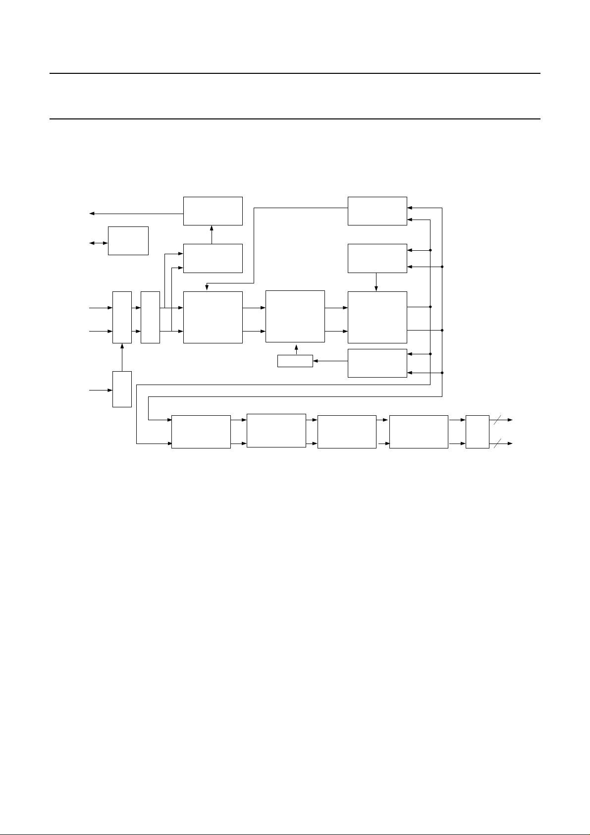
1.2 WITH COMPLEX MULTIPLIER BEFORE ANTI-ALIASING FILTERS (POSMUL=1) :
VAGC
VIN1
VIN2
XIN
I2C
INTERFACE
ADC
Dual 6-bit
PLL
PWM
ENCODER
AGC
DETECTION
COMPLEX
MULTIPLIER
ADC Offset
Cancellation
VITERBI
DECODER
DE-INTERLEAVER
FILTER
BANK
NCO
REED SOLOMON
DECODER
CARRIER
SYNCHRO.
AGC
DETECTION
HALF-NYQUIST
FILTERS
CLOCK
SYNCHRO
DE-SCRAMBLER
Output
Interface
PARALLEL
TS
SERIAL
TS
2000 March 16 4
Page 5
Philips Semiconductors Preliminary specification
yp
Single Chip DVB-S/DSS Channel Receiver TDA10085
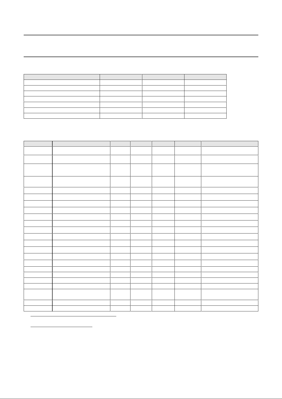
TABLE 1 : ABSOLUTE MAXIMUM RATINGS
Parameter Min Max Unit
Ambient operating temperature (Ta) 0 70 °C
DC supply voltage - 0.5 +4.1 V
DC Core supply voltage t.b.d t.b.d
DC input voltage - 0.5 VDD + 0.5 V
DC input current
Lead Temperature + t.b.d °C
Junction Temperature + t.b.d °C
Stresses above the absolute maximum ratings may cause permanent damage to the device. Exposure to absolute
maximum ratings conditions for extended periods may affect device reliability.
t.b.d
±
TABLE 2: RECOMMENDED OPERATING CONDITIONS
Symbol Parameter Min T
VDDE Digital supply voltage 3.0 3.3 3.6 V 3.3V ±10%
VDDI Digital Core Supply Voltage 1.62 1.8 1.98 V 1.8V ±10%
Max Unit Notes
mA
VDDE5 5V supply voltage
(for 5V Tolerance)
VDD3 3V ADC Digital
supply voltage
Ta Operating temperature 0 70 ° C
AVD Analog supply voltage 3.0 3.3 3.6 V
AVS Analog ground 0 V
VINDC DC Analog Input VREFN VREFP V
VINAC AC Analog Input 750 mVpp
ZIN Analog input impedance t.b.d t.b.d Ohms
CIN Analog input capacitance t.b.d t.b.d t.b.d pF
VREFP Top voltage reference t.b.d V
VREFN Bottom voltage reference t.b.d V
XIN Crystal frequency 4 Mhz MHz
SINAD (1) ADC signal to noise ratio t.b.d dB
THD(2) Total Harmonic Distorsion t.b.d dB
VIH(3) High-level input voltage t.b.d t.b.d V TTL input
VIL Low-level input voltage t.b.d t.b.d V TTL input
VOH(4) High-level output voltage t.b.d V @IOH = -2mA to -4mA
VOL(4) Low-level output voltage t.b.d V @IOL = + 2 mA to +4mA
IDD Supply current t.b.d mA/MBaud @XIN = 4Mhz/
CIN Input capacitance t.b.d pF 1MHz input to VSS
COUT Output capacitance t.b.d pF 1MHz input to VSS
(1) Signal-to-noise plus distortion ratio (SINAD) : ratio between the RMS magnitude of the fundamental input
frequency to the RMS magnitude of all other A/D output signals.
(2) Total harmonic distortion (THD
sample rate) to the fundamental.
(3) All inputs are 5V tolerant except CLB# pin.
(4) IOH, IOL = ±4mA only for pins : OCLK, SDA, SCL_0, SDA_0.
) : ratio of the RMS sum of all harmonics of the input signal (below one half of the
4.5 5 5.5 V pin 25
3.3
96 Mhz Sampling
2000 March 16 5
Page 6

Philips Semiconductors Preliminary specification
Single Chip DVB-S/DSS Channel Receiver TDA10085
FUNCTIONAL DESCRIPTION
PLL
‰
The TDA10085 implements a PLL used as clock multiplier by [M/(N.P)] , so that the crystal can be low frequency
(fundamental tone – typically 4Mhz )
DUAL 6-BIT ADC
‰
The TDA10085 implements a dual 6-bit ADC. The architecture is a standard flash one based on 63 latched
comparators determining simultaneously the precise analog signal level. No external voltage references are
required to use the ADCs.
Furthermore, a new stage was added on the TDA10085 in order to cancel the possible offset generated by the
A./D converter. This is especially important for the very low baud rate applications.
FILTER BANK
‰
The filter bank contains 2 selectable Anti-Alias Low Pass filters (AAF) which, combined with cascadable
decimation filters, allows to perform variable rate demodulation over a ratio of up to 45. An automatic selection of
the filter Gain was added in the TDA10085 in order to facilitate the use of the IC.
COMPLEX MUTIPLIER
‰
Coherent data demodulation (BPSK or QPSK) is performed by complex multiplication of the incoming symbol
with the computed correction angle. This leads to a rotation and a stabilization of the PSK constellation when the
algorithms of carrier and clock recovery have both converged.
The position of this complex multiplier is programmable and can be either after antialiasing filters or before any
filtering.
HALF NYQUIST FILTERS
‰
Half-Nyquist filtering is performed in each arm of the constellation. 2 programmable roll-off are available
depending on the selected standard. The digital filter has 19 (roll-off 0.35) or 25 (roll-off 0.2) taps to provide an
outband attenuation of 40dB.
CARRIER SYNCHRONIZER
‰
The carrier synchronizer block implements successively a phase/frequency comparator, a programmable digital
second order loop filter, a phase accumulator (NCO) that accumulates the phase error and drives a sine/cosine
table to determine the angle for correction, applied to the complex multiplier.
CLOCK SYNCHRONIZER
‰
The clock phase detector block implements the algorithm for variable rate digital timing recovery. The digital
second order loop filter is programmable, and provides an 8-bit command to the NCO block for clock recovery.
AGC
‰
This block calculates the magnitude of the I and Q channels after ADC converter. The value is then compared to
a programmable threshold value, filtered and PWM encoded before being output on the VAGC pin.
Furthermore an internal AGC was added on the Half-Nyquist filters block in order to contr ol the internal dynamic
of the signal.
‰ VITERBI DECODER
The Viterbi decoder performs a maximum likelihood estimation over the received data on the basis of four-bit
quantized samples of the demodulated signals. The average truncation length is 144. The rate R can be chosen
between R = 1/2 and R = 8/9 (punctured codes). Automatic viterbi rate recovery can be selected, so as automatic
spectral inversion ambiguity resolution. The rate search is performed among rates 1/2, 2/3, 3/4, 5/6 and 7/8 In
DVB-S standard and among rates 1/2, 2/3 and 6/7 in DSS mode. Output Bit Error Rate (VBER) is computed by
the RS deocoder. Differential decoding is selectable. The Viterbi decoder provides decoded data and the
corresponding clock.
2000 March 16 6
Page 7

Philips Semiconductors Preliminary specification
Single Chip DVB-S/DSS Channel Receiver TDA10085
FRAME SYNCHRONIZATION AND DEINTERLEAVING
‰
The Viterbi decoder provides errors which occur in bursts. The length of some error bursts may exceed that
which can be reliably corrected by the Reed-Solomon decoder. The implemented de-interleaving is a
convolutional one of depth 12 for DVB and 13 for DSS. The first operation consists in synchronizing the de-
interleaver. This is accomplished by detecting α consecutive sync Words (or
byte of each packet.
Next, the RAM memory associated with the de-interleaver fills up and the first deinterleaved bytes ar e provided
to the input of the Reed-Solomon decoder. The state machine of the de-interleaver goes to the control phase
which counts β consecutive missed sync Words (or
sync ) before declaring the system desynchronized and
going back to the sync. phase. α and β are programmable through the I2C interface.
When the inverted sync word is detected at the input of the de-interleaver (π ambiguity at the input of the Viterbi
decoder), the bytes provided to the Reed-Solomon decoder are inverted at the output of the de-interleaver.
REED-SOLOMON DECODER
‰
The Reed-Solomon decoder decodes the symbol stream from the de-interleaver according to the (N=204 for
DVB and N=146 for DSS) shortened Reed-Solomon code. The Reed-Solomon code is defined over the finite
8
Galois field GF (2
). The field generator polynomial is given by :
sync) which are present as the first
15
0i
=
i
)(xG(x)
+=
This Reed-Solomon decoder corrects up to eight erroneous symbols in each block. When the correction
capability of the decoder is exceeded, the block is not changed and is provided as it has been entered. In this
case the flag UNCOR is set and the MSB of the second byte in the MPEG2 frame is forced to one (TEI :
Transport Error Indicator in DVB-S).The correction capability of the RS decoder can be inhibited.
DESCRAMBLER (DVB-S)
‰
In order to comply with energy dispersal requirements of radio transmission regulations and to ensure adequate
binary transitions, the MPEG2 frames are scrambled at the encoder side. Dual operation is achieved at the
output of the Reed-Solomon decoder using the same scrambler/descrambler. The polynomial for the pseudo
14
random binary sequence (PRBS generator is 1 + x
+ x15). The PRBS registers are initialized at the start of
every eight transport packets. To provide an initialization signal for the descrambler , the MPEG 2 sync byte of the
first transport packet is inverted from 47
to B816. When detected, the descrambler is loaded with the initial
16
sequence "100101010000000". The descrambler can be inhibited. Before being provided, the inverted sync
pattern B8
is reinverted in order to get the original MPEG2 sync word 4716.
16
‰ INTERFACE
A new Output interface was added in the TDA10085 in order to output simultaneously the serial AND parallel
transport stream.
Furthermore, the TDA10085 integrates an I
component I
2
C bus specification.
2
C interface in slave mode. This I2C interface fulfills the Philips
2000 March 16 7
Page 8

Philips Semiconductors Preliminary specification
Single Chip DVB-S/DSS Channel Receiver TDA10085
INPUT – OUTPUT SIGNAL DESCRIPTION
Symbol Pin Number Type Description
CLB# 46 I
XIN
2 I Crystal oscillator input pin. Typically a fundamental XTAL oscillator is
XOUT 1 I Crystal oscillator output pin. Typically a fundamental XTAL oscillator is
PLLGND 6 I Analog ground for the PLL.
PLLVCC 7 I Analog positive supply voltage for the PLL. PLLVCC is typically 3.3V.
DVCC 4 I Digital PLL Core Supply Voltage (typically 1.8V)
DGND 5 I Digital PLL Core Ground Voltage
VAGC 30 OD
CTRL1 21 I/OD ConTRoL line output. This output is directly programmable through the
CTRL2 22 I/OD ConTRoL line output. This output is directly programmable through the
CTRL3 31 I/OD ConTRoL Line input/output. This pin is directly programmable through
DO[7:0] 62,61,60,59,54,
53,52,51
OCLK 50 O Output CLock. OCLK is the output clock for the parallel DO[7:0] outputs.
DEN 49 I/O Data ENable : this output signal is high when there is valid data on bus
UNCOR 48 I/O UNCORrectable packet. This output signal goes high on a rising edge of
PSYNC 47 I/O Packet SYNChro. This output signal goes high on a rising edge of OCLK
FEL 37 OD Front End Locked. This output signal goes high when the demodulator,
The CLB# input is asynchronous and active low, and clears the
3.3V
TDA10085. When CLB# goes low, the circuit immediately enters its
RESET mode and normal operation will resume 3 XIN rising edges later
after CLB# returned high. The I
2
C register contents are all initialized to
their default values. The minimum width of CLB# at low level is 3 XIN
clock periods.
connected between the XIN and XOUT pins.
connected between the XIN and XOUT pins.
PWM encoded output signal for AGC. This signal is typically fed to the
/
AGC amplifier through a single RC network.The maximum signal
O
frequency on VAGC output is SACLK / 4. The refresh frequency of AG C
information is the symbol rate divided by 2048.
This output can be selected by I
2
c to be open drain or 3.3V capable.
I2C interface. Its default value is a logical "1".
CTRL1 is an open drain output and therefore requires an external pullup resistor to either 3.3V or 5V.
I2C interface. Its default value is a logical "0". CTRL2 is an open drain
output and therefore requires an external pull-up resistor to either 3.3V
or 5V.
2
C interface. Its default configuration is an input. A pull-up to 3.3V or
the I
5V, or a pull-down resistor to GND must be connected to CTRL3.
I/O Transport Stream Data Output. These 8-bit parallel data are the outputs
of the TDA10085 after demodulation, Viterbi decoding, de-interleaving,
RS decoding and de-scrambling. There are 3 possible output interfaces :
two parallel and one serial.
OCLK is internally generated depending on which type of interface is
selected.
DO[7:0].
OCLK when the provided packet is uncorrectable.
each time the first byte of a packet is provided.
the Viterbi decoder and the de-interleaver are all synchronized. FEL is
an open drain output and therefore requires an external pull up resistor
to either 3.3V or 5V.
Furthermore the FEL pin can be set by I
2
C to be the interrupt pin.
2000 March 16 8
Page 9

Philips Semiconductors Preliminary specification
Single Chip DVB-S/DSS Channel Receiver TDA10085
TMD 18 I TEST input. This input pin must be grounded for normal operation of the
TDA10085.
ENSERI 19 I ENable SERIal : When High, the Serial Tr ansport Stream is present on
the Boundary Scan Pin (TRST, TDO, TCK, TDI, TMS). When low the BS
pins are available.
TRST 36 I/O Test ReSeT. This active low input signal is used to reset the TAP
controller when in boundary scan mode.
In normal mode of operation TRST must be set low.
In Serial Mode (ENSERI=1), TRST is the psync output.
TDO 45 O Test Data Out. This is the serial Test output pin used in boundary scan
mode. Serial Data are provided on the falling edge of TCK.
In Serial Mode (ENSERI=1), TDO is the enable output.
TCK 35 I/O Test ClocK : an independant clock used to drive the TAP controller when
in boundary scan mode.
In normal mode of operation, TCK must be grounded.
In Serial Mode (ENSERI=1), TCK is the clock output.
TDI 40 I/O Test Data In. The serial input for Test data and instruction when in
boundary scan mode. In normal mode of operation, TDI must be set to
GND or VDDx
In Serial Mode (ENSERI=1), TDI is the data output.
TMS 34 I/O Test Mode Select. This input signal provides the logic levels needed to
change the TAP controller from state to state.
In normal mode of operation, TMS must be set to VDD.
In Serial Mode (ENSERI=1), TMS is the uncorrectable output..
SADDR0 17 I SADDR0 input signal is the LSB of the I2C address of the
TDA10085.The MSBs are internally set to 000111. Therefore the
complete I2C address of the TDA10085 is (MSB to LSB) : 0, 0, 0, 1, 1,
1, SADDR0.
SDA 32 I/OD SDA is a bidirectional signal. It is the serial input/output of the I2C
internal block. A pull-up resistor (typically 2.2 k•) must be connected
between SDA and 5V for proper operation (Open Drain output).
SCL 33 I I2C clock input. SCL should nominally be a square wave with a
maximum frequency of 400 KHz. SCL is generated by the system I2C
master.
IICDIV 20 I IICDIV allows to select the frequency of the I2C internal system clock,
depending on the crystal frequency. Internal I2C clock is a division of
XIN by 4
VIN1 15 I Analog signal Input for channel I.
VIN2 12 I Analog signal Input for channel Q.
VREFN 14 O Analog negative voltage reference. A decoupling capacitor of typically
0.1µF must be placed as close as possible between VREFN and GND.
The typical voltage value at VREFN is 1.25V.
VREFP 13 O Analog positive voltage reference. A decoupling capacitor of typically 0.1
µF must be placed as closed as possible between VREFP and GND.
The typical voltage value at VREFP is 2V.
AVD 16 I
AVS 11 I Analog ground voltage.
Analog positive supply voltage. AVD is typically 3.3V. A 0.1µF
decoupling capacitor must be placed between AVD and AVS.
IICDIV
and must be between 4 and 20 MHz..
2000 March 16 9
Page 10
Philips Semiconductors Preliminary specification
Single Chip DVB-S/DSS Channel Receiver TDA10085
SCL_0 29 OD This output is equivalent to the SCL input, but can be tristated by I2C
programmation. A pull-up resistor (typically 22KΩ) must be connected
between this pin and 5V.
SDA_0 28 I/OD This signal is equivalent to the SDA I/O of the TDA10085 but can be
tristated by I2C programmation. SDA_0 is bidirectionnal. A pull-up
resistor (typically 22KΩ) must be connected between this pin and VCC.
22K 63 O
VSSI 8,23,39,56,64 I Digital Core ground voltage.
VDDI 3,9,24,38,55 I Digital Core supply voltage.(Typically 1.8V)_
VSSE 26,44,58 I Digital ground voltage
VDDE 27,43,57 I Digital supply voltage.(Typically 3.3V)_
VDDE5 25 I Digital 5V supply voltage.(for the 5V Tolerance)
VDD3 10 I Analog 3.3 Suply Voltage for the A/D Converter
ADVD 42 I Analog Supply Voltage for the 2nd PLL (typically 1.8V)
ADVS 41 I Analog Ground Voltage for the 2nd PLL.
This output pin provides the 22KHz used to control the antena LNB. This
3.3V
output is controlled via the I2C interface.
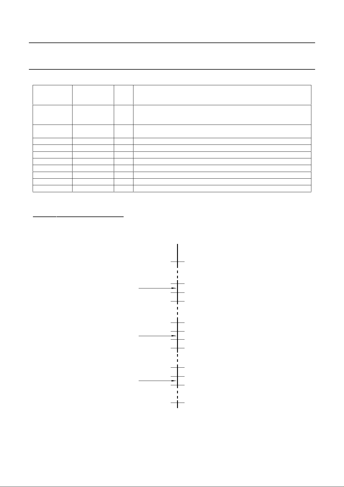
TABLE 3. I,Q INPUT FORMAT
This table is to be used with an external 6-bit ADC.
Offset binary 2’s complement
1 1 1 1 1 1 0 1 1 1 1 1
1 1 0 0 0 0 0 1 0 0 0 0
+ 1
1 0 1 1 1 1 0 0 1 1 1 1
1 0 1 1 1 0 0 0 1 1 1 0
1 0 0 0 0 1 0 0 0 0 0 1
1 0 0 0 0 0 0 0 0 0 0 0
zero
0 1 1 1 1 1 1 1 1 1 1 1
0 1 1 1 1 0 1 1 1 1 1 0
0 1 0 0 0 1 1 1 0 0 0 1
0 1 0 0 0 0 1 1 0 0 0 0
- 1
0 0 1 1 1 1 1 0 1 1 1 1
(IFS = 0) (IFS = 1)
0 0 0 0 0 0 1 0 0 0 0 0
Note : (+1) and (-1) levels correspond to AGCR[4:0] set to B16.
2000 March 16 10
Page 11

Philips Semiconductors Preliminary specification
Single Chip DVB-S/DSS Channel Receiver TDA10085
TABLE 4. PUNCTURING AND MAPPING
Rate R Inhibition Flags Mapping
1/2 000 inh[0] = 1
inh[1] = 1
2/3 001 inh[0] = 10 10
inh[1] = 11 11
3/4 010 inh[0] = 101
inh[1] = 110
4/5 011 inh[0] = 1000 1000
inh[1] = 1111 1111
5/6 100 inh[0] = 10101
inh[1] = 11010
6/7 101 inh[0] = 100101 100101
inh[1] = 111010 111010
7/8 110 inh[0] = 1000101
inh[1] = 1111010
8/9 111 inh[0] = 10001011 10001011
inh[1] = 11110100 11110100
I = X1
Q = Y1
I = X1Y2Y3
Q = Y1X3Y4
I = X1Y2
Q = Y1X3
I = X1Y2Y4Y5Y7
Q = Y1Y3X5Y6Y8
I = X1Y2Y4
Q = Y1X3X5
I = X1Y2X4X6Y7Y9Y11
Q = Y1Y3Y5X7Y8X10 X12
I = X1Y2X4Y6
Q = Y1Y3X5X7
I = X1Y2Y4Y6X8Y9Y11X13X15
Q = Y1Y3X5X7X9Y10Y12Y14X16
Notes :
1.Polynomial X is G1=171 inhibited with inh[0]
2.Polynomial Y is G2=133 inhibited with inh[1]
3.In DVB and RAUTO modes, the only Viterbi rates that the internal state machine will look for synchronization are :
1/2, 2/3, 3/4, 5/6 and 7/8.
4.In DSS and RAUTO modes, the only Viterbi rates that the internal state machine will look for synchronization are :
1/2, 2/3 and 6/7.
2000 March 16 11
Page 12
Philips Semiconductors Preliminary specification
Single Chip DVB-S/DSS Channel Receiver TDA10085
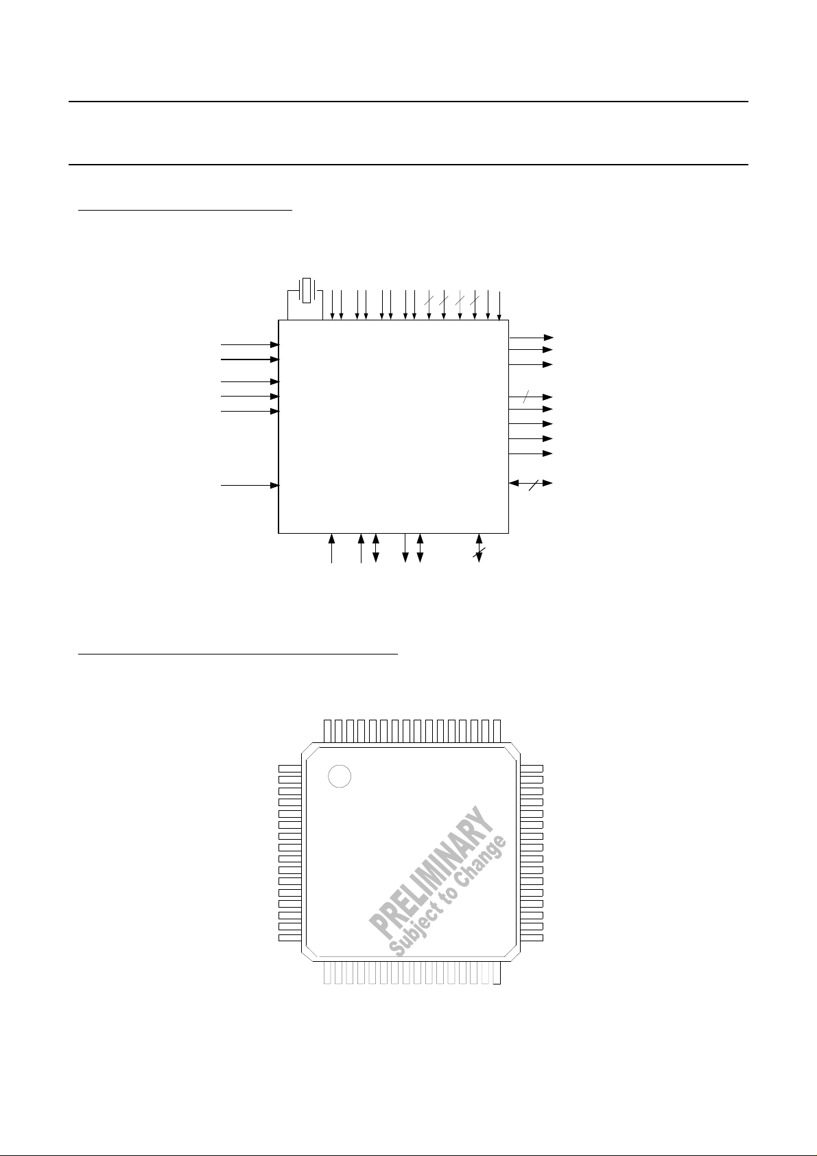
FIGURE 2. BLOCK DIAGRAM
VDDI
VDDE
PLLVCC
DVCC
ADVS
AVS
AVD
ADVD
DGND
PLLGND
VSSE
33
5
VSSI
VDDE5
5
VDD3
XIN XOUT
VIN1
VIN2
CLB#
ENSERI
TMD
IICDIV
INPUTS OUTPUTS
SADDR0
TDA10085
I2C INTERFACE
SCL SDA SCL_O SDA_O
FIGURE 3. PIN CONFIGURATION (64 TQFP)
22K
VSSI
DO[7]
DO[6]
DO[5]
POWER SUPPLIES
DO[4]
VSSE
VDDE
VSSI
VDDI
VAGC
FEL/INT
22K
8
DO
DEN
OCLK
PSYNC
UNCOR
5
BS/
SERIAL TS
3
CTRL
OCLK
DO[3]
DO[2]
DEN
DO[1]
DO[0]
64
XOUT
1
XIN
VDDI
DVCC
DGND
PLLGND
PLLVCC
TDA10085
TQFP 64
VSSI
VDDI
VDD3
AVS
VIN2
VREFP
VREFN
VIN1
AVD
16
TMD
ENSERI
SADDR0
VSSI
IICDIV
CTRL1
CTRL2
2000 March 16 12
49
48
UNCOR
PSYNC
CLB
TDO
VSSE
VDDE
ADVD
ADVS
TDI
VSSI
VDDI
FEL
TRST
TCK
33
3217
VDDI
VSSE
VDDE
VDDE5
SDA_O
SDA
VAGC
CTRL4
SCL_O
TMS
SCL
Page 13

Philips Semiconductors Preliminary specification
Single Chip DVB-S/DSS Channel Receiver TDA10085
TABLE 5. PIN DESCRIPTION
Pin Pin Name Type Pin Pin Name Type
1 XOUT I 34 TMS I/O
2 XIN I 35 TCK I/O
3 VDDI - 36 TRST I/O
4DVCC- 37 FELOD
5 DGND - 38 VDDI 6 PLLGND - 39 VSSI 7 PLLVCC - 40 TDI I/O
8 VSSI - 41 ADVS -
9 VDDI - 42 ADVD 10 VDD3 - 43 VDDE 11 AVS - 44 VSSE 12 VIN2 I 45 TDO O
13 VREFP O 46 CLB# I
14 VREFN O 47 PSYNC I/O
15 VIN1 I 48 UNCOR I/O
16 AVD - 49 DEN I/O
17 SADDRO I 50 OCLK O
18 TMD I 51 DO[0] I/O
19 ENSERI I 52 DO[1] I/O
20 IICDIV I 53 DO[2] I/O
21 CTRL1 I/OD 54 DO[3] I/O
22 CTRL2 I/OD 55 VDDI 23 VSSI - 56 VSSI 24 VDDI - 57 VDDE 25 VDDE5 - 58 VSSE 26 VSSE - 59 DO[4] I/O
27 VDDE - 60 DO[5] I/O
28 SDA_0 I/OD 61 DO[6] I/O
29 SCL_0 OD 62 DO[7] I/O
30 VAGC O or OD 63 22K I/O
31 CTRL3 I/OD 64 VSSI 32 SDA I/OD
33 SCL I
Notes :
1.All inputs (I) are TTL, 5V tolerant inputs except CLB# pin.
2.OD are Open Drain 5V outputs, so they must be connected to a pull-up resistor to either 3.3V or 5V.
3. DGND, VSSI and VSSE can be connected to the same GND ground.
2000 March 16 13
Page 14
Philips Semiconductors Preliminary specification
Single Chip DVB-S/DSS Channel Receiver TDA10085
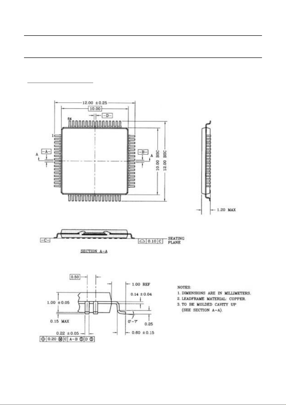
PACKAGE DESCRIPTION
2000 March 16 14
Page 15

Philips Semiconductors Preliminary specification
Single Chip DVB-S/DSS Channel Receiver TDA10085
DATA SHEET STATUS
DATA SHEET STATUS
PRODUCT
STATUS
DEFINITIONS
(1)
Objective specification Development This data sheet contains the design target or goal specifications for
product development. Specification may change in any manner without
notice.
Preliminary specification Qualification This data sheet contains preliminary data, and supplementary data will be
published at a later date. Philips Semiconductors reserves the right to
make changes at any time without notice in order to improve design and
supply the best possible product.
Product specification Production This data sheet contains final specifications. Philips Semiconductors
reserves the right to make changes at any time without notice in order to
improve design and supply the best possible product.
Note
1. Please consult the most recently issued data sheet before initiating or completing a design.
DEFINITIONS
Short-form specification The data in a short-form
specification is extracted from a full data sheet with the
same type number and title. For detailed information see
the relevant data sheet or data handbook.
Limiting values definition Limiting values given are in
accordance with the Absolute Maximum Rating System
(IEC 60134). Stress above one or more of the limiting
values may cause permanent damage to the device.
These are stress ratings only and operation of the device
attheseoratany other conditions above those given in the
Characteristics sections of the specification is not implied.
Exposure to limiting values for extended periods may
affect device reliability.
Application information Applications that are
described herein for any of these products are for
illustrative purposes only. Philips Semiconductors make
norepresentationorwarrantythatsuchapplicationswillbe
suitable for the specified use without further testing or
modification.
DISCLAIMERS
Life support applications These products are not
designed for use in life support appliances, devices, or
systems where malfunction of these products can
reasonably be expected to result in personal injury. Philips
Semiconductorscustomersusingorsellingtheseproducts
for use in such applications do so at their own risk and
agree to fully indemnify Philips Semiconductors for any
damages resulting from such application.
Right to make changes Philips Semiconductors
reserves the right to make changes, without notice, in the
products, including circuits, standard cells, and/or
software, described or contained herein in order to
improve design and/or performance. Philips
Semiconductors assumes no responsibility or liability for
theuseofanyoftheseproducts,conveysnolicenceortitle
under any patent, copyright, or mask work right to these
products,andmakes no representations or warranties that
these products are free from patent, copyright, or mask
work right infringement, unless otherwise specified.
2
PURCHASE OF PHILIPS I
C COMPONENTS
Purchase of Philips I
2
C components conveys a license under the Philips’ I2C patent to use the
components in the I2C system provided the system conforms to the I2C specification defined by
Philips. This specification can be ordered using the code 9398 393 40011.
2000 March 16 15
Page 16

Philips Semiconductors – a w orldwide compan y
Argentina: see South America
Australia: 3 Figtree Drive, HOMEBUSH, NSW 2140,
Tel. +61 2 9704 8141, Fax. +61 2 9704 8139
Austria: Computerstr. 6, A-1101 WIEN, P.O. Box 213,
Tel. +43 1 60 101 1248, Fax. +43 1 60 101 1210
Belarus: Hotel Minsk Business Center, Bld. 3, r. 1211, Volodarski Str. 6,
220050 MINSK, Tel. +375 172 20 0733, Fax. +375 172 20 0773
Belgium: see The Netherlands
Brazil: see South America
Bulgaria: Philips Bulgaria Ltd., Energoproject, 15th floor,
51 James Bourchier Blvd., 1407 SOFIA,
Tel. +359 2 68 9211, Fax. +359 2 68 9102
Canada: PHILIPS SEMICONDUCTORS/COMPONENTS,
Tel. +1 800 234 7381, Fax. +1 800 943 0087
China/Hong Kong: 501 Hong Kong Industrial Technology Centre,
72 Tat Chee Avenue, Kowloon Tong, HONG KONG,
Tel. +852 2319 7888, Fax. +852 2319 7700
Colombia: see South America
Czech Republic: see Austria
Denmark: Sydhavnsgade 23, 1780 COPENHAGEN V,
Tel. +45 33 29 3333, Fax. +45 33 29 3905
Finland: Sinikalliontie 3, FIN-02630 ESPOO,
Tel. +358 9 615 800, Fax. +358 9 6158 0920
France: 51 Rue Carnot, BP317, 92156 SURESNES Cedex,
Tel. +33 1 4099 6161, Fax. +33 1 4099 6427
Germany: Hammerbrookstraße 69, D-20097 HAMBURG,
Tel. +49 40 2353 60, Fax. +49 40 2353 6300
Hungary: see Austria
India: Philips INDIA Ltd, Band Box Building, 2nd floor,
254-D, Dr. Annie Besant Road, Worli, MUMBAI 400 025,
Tel. +91 22 493 8541, Fax. +91 22 493 0966
Indonesia: PTPhilips DevelopmentCorporation,Semiconductors Division,
Gedung Philips, Jl. Buncit Raya Kav.99-100, JAKARTA 12510,
Tel. +62 21 794 0040 ext. 2501, Fax. +62 21 794 0080
Ireland: Newstead, Clonskeagh, DUBLIN 14,
Tel. +353 1 7640 000, Fax. +353 1 7640 200
Israel: RAPAC Electronics, 7 Kehilat Saloniki St, PO Box 18053,
TEL AVIV 61180, Tel. +972 3 645 0444, Fax. +972 3 649 1007
Italy: PHILIPS SEMICONDUCTORS,ViaCasati, 23 - 20052 MONZA (MI),
Tel. +39 039 203 6838, Fax +39 039 203 6800
Japan: Philips Bldg 13-37, Kohnan 2-chome, Minato-ku,
TOKYO 108-8507, Tel. +81 3 3740 5130, Fax. +81 3 3740 5057
Korea: Philips House, 260-199 Itaewon-dong, Yongsan-ku, SEOUL,
Tel. +82 2 709 1412, Fax. +82 2 709 1415
Malaysia: No. 76 Jalan Universiti, 46200 PETALING JAYA, SELANGOR,
Tel. +60 3 750 5214, Fax. +60 3 757 4880
Mexico: 5900 Gateway East, Suite 200, EL PASO, TEXAS 79905,
Tel. +9-5 800 234 7381, Fax +9-5 800 943 0087
Middle East: see Italy
Netherlands: Postbus 90050, 5600 PB EINDHOVEN, Bldg. VB,
Tel. +31 40 27 82785, Fax. +31 40 27 88399
New Zealand: 2 Wagener Place, C.P.O. Box 1041, AUCKLAND,
Tel. +64 9 849 4160, Fax. +64 9 849 7811
Norway: Box 1, Manglerud 0612, OSLO,
Tel. +47 22 74 8000, Fax. +47 22 74 8341
Pakistan: see Singapore
Philippines: Philips Semiconductors Philippines Inc.,
106 Valero St. Salcedo Village, P.O. Box 2108 MCC, MAKATI,
Metro MANILA, Tel. +63 2 816 6380, Fax. +63 2 817 3474
Poland: Al.Jerozolimskie 195 B, 02-222 WARSAW,
Tel. +48 22 5710 000, Fax. +48 22 5710 001
Portugal: see Spain
Romania: see Italy
Russia: Philips Russia, Ul. Usatcheva 35A, 119048 MOSCOW,
Tel. +7 095 755 6918, Fax. +7 095 755 6919
Singapore: Lorong 1, Toa Payoh, SINGAPORE 319762,
Tel. +65 350 2538, Fax. +65 251 6500
Slovakia: see Austria
Slovenia: see Italy
South Africa: S.A. PHILIPS Pty Ltd., 195-215 Main Road Martindale,
2092 JOHANNESBURG, P.O. Box 58088 Newville 2114,
Tel. +27 11 471 5401, Fax. +27 11 471 5398
South America: Al. Vicente Pinzon, 173, 6th floor,
04547-130 SÃO PAULO, SP, Brazil,
Tel. +55 11 821 2333, Fax. +55 11 821 2382
Spain: Balmes 22, 08007 BARCELONA,
Tel. +34 93 301 6312, Fax. +34 93 301 4107
Sweden: Kottbygatan 7, Akalla, S-16485 STOCKHOLM,
Tel. +46 8 5985 2000, Fax. +46 8 5985 2745
Switzerland: Allmendstrasse 140, CH-8027 ZÜRICH,
Tel. +41 1 488 2741 Fax. +41 1 488 3263
Taiwan: Philips Semiconductors, 5F, No. 96, Chien Kuo N. Rd., Sec. 1,
TAIPEI, Taiwan Tel. +886 2 2134 2451, Fax. +886 2 2134 2874
Thailand: PHILIPS ELECTRONICS (THAILAND) Ltd.,
60/14 MOO 11, Bangna Trad Road KM. 3, Bagna, BANGKOK 10260,
Tel. +66 2 361 7910, Fax. +66 2 398 3447
Turkey: Yukari Dudullu, Org. San. Blg., 2.Cad. Nr. 28 81260 Umraniye,
ISTANBUL, Tel. +90 216 522 1500, Fax. +90 216 522 1813
Ukraine: PHILIPS UKRAINE, 4 Patrice Lumumba str., Building B, Floor 7,
252042 KIEV, Tel. +380 44 264 2776, Fax. +380 44 268 0461
United Kingdom: Philips Semiconductors Ltd., 276 Bath Road, Hayes,
MIDDLESEX UB3 5BX, Tel. +44 208 730 5000, Fax. +44 208 754 8421
United States: 811 East Arques Avenue, SUNNYVALE, CA 94088-3409,
Tel. +1 800 234 7381, Fax. +1 800 943 0087
Uruguay: see South America
Vietnam: see Singapore
Yugoslavia: PHILIPS, Trg N. Pasica 5/v, 11000 BEOGRAD,
Tel. +381 11 3341 299, Fax.+381 11 3342 553
For all other countries apply to: Philips Semiconductors,
Marketing Communications, Building BE-p, P.O. Box 218, 5600 MD EINDHOVEN,
The Netherlands, Fax. +31 40 27 24825
© Philips Electronics N.V. SCA
All rights are reserved. Reproduction in whole or in part is prohibited without the prior written consent of the copyright owner.
The information presented in this document does not form part of any quotation or contract, is believed to be accurate and reliable and may be changed
without notice. No liability will be accepted by the publisher for any consequence of its use. Publication thereof does not convey nor imply any license
under patent- or other industrial or intellectual property rights.
2000
Internet: http://www.semiconductors.philips.com
70
Printed in The Netherlands 753504/03/pp16 Date of release: 2000 March 16 Document order number: 9397 750 07146
 Loading...