

Page 1
Order this document by TCF6000/D
The TCF6000 was designed to protect input/output lines of
microprocessor systems against voltage transients.
• Optimized for HMOS System
• Minimal Component Count
• Low Board Space Requirement
• No P.C.B. Track Crossovers Required
• Applications Areas Include Automotive, Industrial,
Telecommunications and Consumer Goods
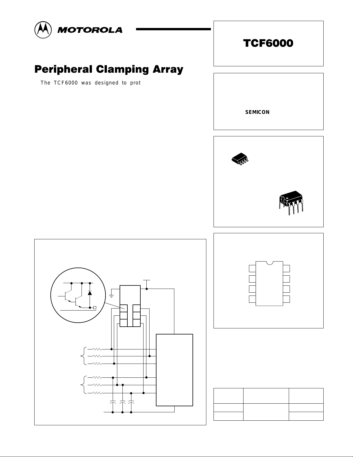
Figure 1. Representative Block Diagram and
Simplified Application
V
V
CC
V
Gnd
Ref
Generator
V
Ref
Pin
DD
PERIPHERAL CLAMPING
ARRAY
SEMICONDUCTOR
TECHNICAL DATA
D SUFFIX
PLASTIC PACKAGE
8
1
NO SUFFIX
PLASTIC PACKAGE
CASE 626
PIN CONNECTIONS
Gnd
1
2
Clamp
3
Clamp
45
Clamp
CASE 751
(SO–8)
V
8
CC
7
Clamp
6
Clamp
Clamp
Gnd
Each Cell
Digital
Inputs
Analog
Inputs
R
in
Gnd
MOTOROLA ANALOG IC DEVICE DATA
Micro
Computer
ORDERING INFORMATION
Operating
C
in
Device
TCF6000D
TCF6000
Motorola, Inc. 1996 Rev 0
Temperature Range
TA = – 40° to +85°C
Package
SO–8
Plastic DIP
1
Page 2
TCF6000
MAXIMUM RATINGS
Supply Voltage V
Supply Current I
Clamping Current I
Junction Temperature T
Power Dissipation (TA = + 85°C) P
Thermal Resistance (Junction–Ambient) θ
Operating Ambient Temperature Range T
Storage Temperature Range T
NOTE: 1. Values beyond which damage may occur .
ELECTRICAL CHARACTERISTICS (T
Positive Clamping Voltage (Note 2)
(IIK = 10 mA, –40°C ≤ TA ≤ + 85°C)
Positive Peak Clamping Current I
Negative Peak Clamping Voltage
(IIK = –10 mA, –40°C ≤ TA ≤ + 85°C)
Negative Peak Clamping Current I
Output Leakage Current
(0 V ≤ Vin ≤ VCC)
(0 V ≤ Vin ≤ VCC, –40°C ≤ TA ≤ + 85°C)
Channel Crosstalk (ACT = 20 log IL/IIK) A
Quiescent Current (Package) I
NOTE: 2. The device might not give 100% protection in CMOS applications.
(TA = 25°C, unless otherwise noted, Note 1.)
Rating
Characteristics
Symbol Value Unit
CC
i
IK
J
D
JA
A
stg
= 25°C, 4.5 ≤ VCC ≤ 5.5 V, unless otherwise noted.)
A
6.0 V
300 mA
±50 mA
150 °C
400 m/W
100 °C/W
–40 to +85 °C
–55 to + 150 °C
Symbol Min Max Unit
V
(IK)
IK(P)
V
(IK)
IK(P)
I
L
I
LT
CT
B
– VCC + 1.0 V
– 20 mA
–0.3 – V
–20 – mA
–
–
100 – dB
– 2.0 mA
1.0
5.0
µA
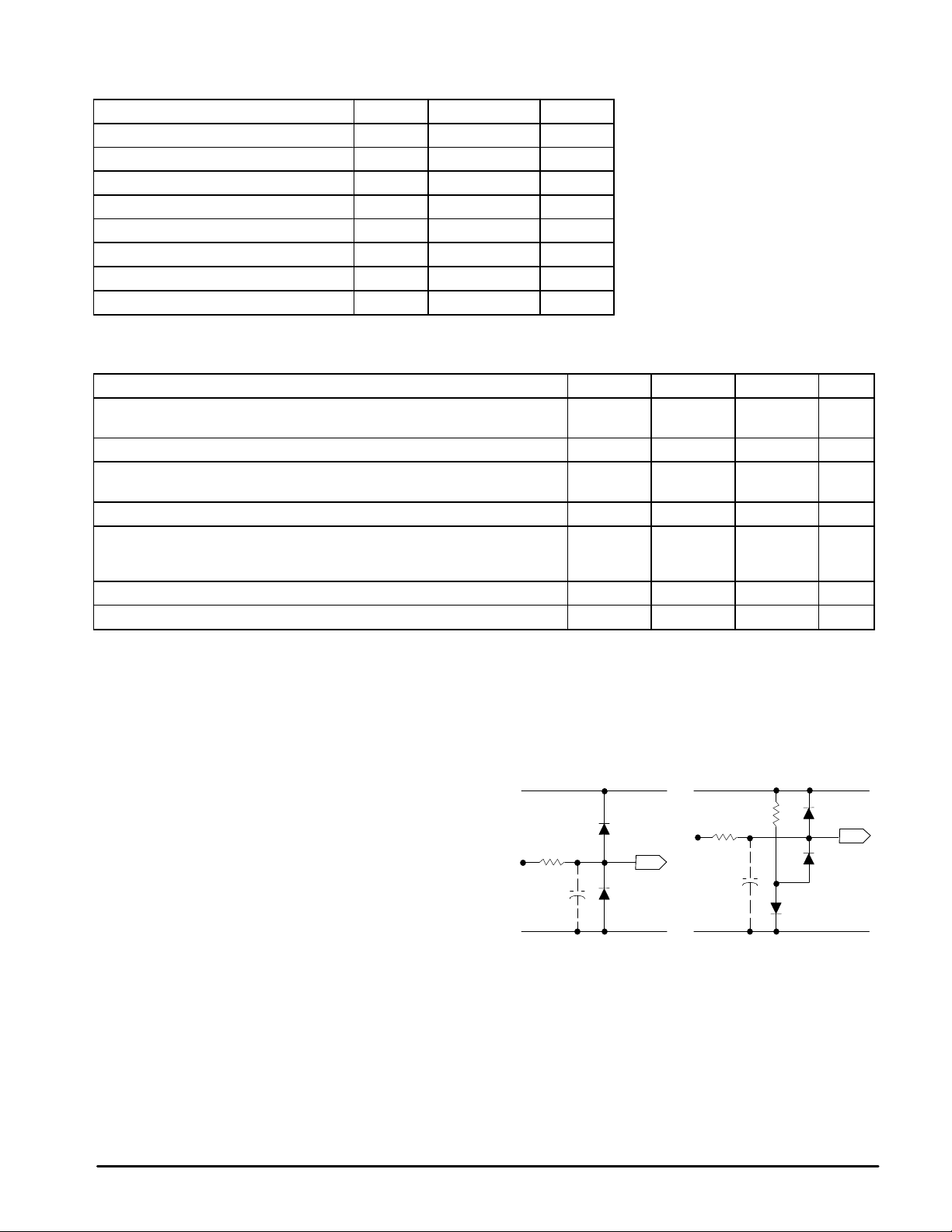
CIRCUIT DESCRIPTION
To ensure the reliable operation of any integrated circuit
based electronics system, care has been taken that voltage
transients do not reach the device I/O pins. Most NMOS,
HMOS and Bipolar integrated circuits are particularly
sensitive to negative voltage peaks which can provoke
latch–up or otherwise disturb the normal functioning of the
circuit, and in extreme cases may destroy the device.
Generally the maximum rating for a negative voltage
transients on integral circuits is –0.3 V over the whole
temperature range. Classical protection units have consisted
of diode/resistor networks as shown in Figures 2a and 2b.
The arrangement in Figure 2a does not, in general, meet
the specification and is therefore inadequate.
The problem with the solution shown if Figure 2b lies
mainly with the high current drain through the biassing
devices R1 and D3. A second problem exists if the input line
carries an analog signal. When Vin is close to the ground
potential, currents arising from leakage and mismatch
between D3 and D2 can be sourced into the input line, thus
disturbing the reading.
Figure 2. Classical Protection Circuits
(a) (b)
VinR
V
CC
D1
in
C
in
µ
D2
Gnd Gnd
VinR
C
R1
in
C
in
V
CC
D1
µ
C
D2
D
3
Figure 3 shows the clamping characteristics which
are common to each of the six cells in the Peripheral
Clamping Array.
As with the classical protection circuits, positive voltage
transients are clamped by means of a fast diode to the V
supply line.
CC
2
MOTOROLA ANALOG IC DEVICE DATA
Page 3

Figure 3. Clamping Characteristics
I
IK
+10 mA
–0.3 V
Low
Impedance
0 V
–10 mA
High Low
Impedance Impedance
TCF6000
APPLICATIONS INFORMATION
Figure 4 depicts a typical application in a microcomputer
based automotive ignition system.
The TCF6000 is being used not only to protect the
system’s normal inputs but also the (bidirectional) serial
diagnostics port.
The value of the input resistors, Rin, is determined by the
clamping current and the anticipated value of the spikes.
V
CC
0.75 V Typ
VCC+
V
in
Thus:
V
where:
So, taking,
gives,
Rin =
= Peak Volts (V)
V
= Clamping current (A)
I
IK
= 300 V typically (SAE J1211)
V
= 10 mA (recommended)
I
IK
= 30 k
R
in
Ω
I
IK
Resistors of this value will not usually cause any problems
in MOS systems, but their presence needs to be taken into
account by the designer. Their ef fect will normally need to be
compensated for Bipolar systems.
V
bat
Gnd
V
bat
Pick Up
Temperature
Pressure
Gnd
Hall
Effect
Engine
Sensor
Battery
Volts
Figure 4. T ypical Automotive Application
V
CC
Gnd
R
Hall
6X
R
in
TCF6000
3X
C
in
Gnd
V
CC
INT1
D1
MC6805S2
D0
D2
V
SS
Gnd
Serial Diagnostics
B0
D6
B1
B2
Coil Drive
Coil Feedback
MOTOROLA ANALOG IC DEVICE DATA
Ignition ModuleCar
3
Page 4

TCF6000
The use of Cin is not mandatory , and is not recommended
where the lines to be protected are used for output or for both
input and output. For digital input lines, the use of a small
capacitor in the range of 50 pF to 220 pF is recommended as
this will reduce the rate of rise of voltage seen by the
TCF6000 and hence the possibility of overshoot.
In the case of the analog inputs, such as that from the
pressure sensor, the capacitor Cin is necessary for devices
such as the MC6805S2 shown, which present a low
impedance during the sampling period. The maximum value
for Cin is determined by the accuracy required, the time taken
to sample the input and the input impedance during that time,
while the maximum value is determined by the required
frequency response and the value of R
Thus for a resistive input A/D connector where:
= Sample time (seconds)
T
s
= Device input resistance (Ω)
R
D
= Input voltage (V)
V
in
= Required accuracy (%)
k
= Charge on capacitor before sampling
Q
1
= Charge on capacitor after sampling
Q
2
= Device input current (A)
I
D
in.
kQ
Thus:
but,
and,
so that, ID Ts =
and, Cin (min) =
so, Cin (min) =
even simpler:
k
C
Cin (min) =
For the MC6805S2 this comes out at:
Cin (min) =
Q1–Q2 =
= Cin V
Q
1
= ID• T
Q1–Q
2
The calculation for a sample and hold type converter is
= Required accuracy (%)
= Hold capacitor (Farad)
H
100 • C
k
100.25 pF
0.25
1
100
in
s
k • Cin–V
ID• T
Vin• k
100 • T
k • R
H
in
100
s
Farad
s
Farad
D
Farad
= 10 nF for 1/4% accuracy
4
MOTOROLA ANALOG IC DEVICE DATA
Page 5

NOTE 2
–T–
SEATING
PLANE
H
58
–B–
14
F
–A–
C
N
D
K
G
0.13 (0.005) B
M
T
TCF6000
OUTLINE DIMENSIONS
PLASTIC PACKAGE
CASE 626–05
ISSUE K
L
J
M
M
A
M
NOTES:
1. DIMENSION L TO CENTER OF LEAD WHEN
FORMED PARALLEL.
2. PACKAGE CONTOUR OPTIONAL (ROUND OR
SQUARE CORNERS).
3. DIMENSIONING AND TOLERANCING PER ANSI
Y14.5M, 1982.
DIM MIN MAX MIN MAX
A 9.40 10.16 0.370 0.400
B 6.10 6.60 0.240 0.260
C 3.94 4.45 0.155 0.175
D 0.38 0.51 0.015 0.020
F 1.02 1.78 0.040 0.070
G 2.54 BSC 0.100 BSC
H 0.76 1.27 0.030 0.050
J 0.20 0.30 0.008 0.012
K 2.92 3.43 0.115 0.135
L 7.62 BSC 0.300 BSC
M ––– 10 ––– 10
N 0.76 1.01 0.030 0.040
INCHESMILLIMETERS
__
–T–
–A–
58
4X P
–B–
14
G
C
SEATING
PLANE
8X D
K
0.25 (0.010)MB
SS
A0.25 (0.010)MTB
D SUFFIX
PLASTIC PACKAGE
CASE 751–05
ISSUE N
M
R
X 45
_
M
(SO–8)
_
NOTES:
1. DIMENSIONING AND TOLERANCING PER
ANSI Y14.5M, 1982.
2. CONTROLLING DIMENSION: MILLIMETER.
3. DIMENSIONS A AND B DO NOT INCLUDE
MOLD PROTRUSION.
4. MAXIMUM MOLD PROTRUSION 0.15 (0.006)
PER SIDE.
5. DIMENSION D DOES NOT INCLUDE DAMBAR
PROTRUSION. ALLOWABLE DAMBAR
PROTRUSION SHALL BE 0.127 (0.005) TOTAL
IN EXCESS OF THE D DIMENSION AT
MAXIMUM MATERIAL CONDITION.
DIM MIN MAX MIN MAX
A 4.80 5.00 0.189 0.196
F
J
B 3.80 4.00 0.150 0.157
C 1.35 1.75 0.054 0.068
D 0.35 0.49 0.014 0.019
F 0.40 1.25 0.016 0.049
G 1.27 BSC 0.050 BSC
J 0.18 0.25 0.007 0.009
K 0.10 0.25 0.004 0.009
M 0 7 0 7
P 5.80 6.20 0.229 0.244
R 0.25 0.50 0.010 0.019
INCHESMILLIMETERS
____
MOTOROLA ANALOG IC DEVICE DATA
5
Page 6

TCF6000
Motorola reserves the right to make changes without further notice to any products herein. Motorola makes no warranty , representation or guarantee regarding
the suitability of its products for any particular purpose, nor does Motorola assume any liability arising out of the application or use of any product or circuit, and
specifically disclaims any and all liability, including without limitation consequential or incidental damages. “T ypical” parameters which may be provided in Motorola
data sheets and/or specifications can and do vary in different applications and actual performance may vary over time. All operating parameters, including “Typicals”
must be validated for each customer application by customer’s technical experts. Motorola does not convey any license under its patent rights nor the rights of
others. Motorola products are not designed, intended, or authorized for use as components in systems intended for surgical implant into the body, or other
applications intended to support or sustain life, or for any other application in which the failure of the Motorola product could create a situation where personal injury
or death may occur. Should Buyer purchase or use Motorola products for any such unintended or unauthorized application, Buyer shall indemnify and hold Motorola
and its officers, employees, subsidiaries, affiliates, and distributors harmless against all claims, costs, damages, and expenses, and reasonable attorney fees
arising out of, directly or indirectly, any claim of personal injury or death associated with such unintended or unauthorized use, even if such claim alleges that Motorola
was negligent regarding the design or manufacture of the part. Motorola and are registered trademarks of Motorola, Inc. Motorola, Inc. is an Equal
Opportunity/Affirmative Action Employer.
How to reach us:
USA/EUROPE/Locations Not Listed: Motorola Literature Distribution; JAPAN: Nippon Motorola Ltd.; Tatsumi–SPD–JLDC, 6F Seibu–Butsuryu–Center,
P.O. Box 20912; Phoenix, Arizona 85036. 1–800–441–2447 or 602–303–5454 3–14–2 T atsumi Koto–Ku, Tokyo 135, Japan. 03–81–3521–8315
MFAX: RMF AX0@email.sps.mot.com – TOUCHT ONE 602–244–6609 ASIA/PACIFIC: Motorola Semiconductors H.K. Ltd.; 8B Tai Ping Industrial Park,
INTERNET: http://Design–NET.com 51 Ting Kok Road, Tai Po, N.T., Hong Kong. 852–26629298
6
◊
MOTOROLA ANALOG IC DEVICE DATA
TCF6000/D
*TCF6000/D*
 Loading...