

Page 1
Dual Power Operational Amplifier
TCA 2465
Overview Bipolar IC
Features
• High output peak current of twice 2.5 A
• Twice 2.0 A output peak current for TCA 2465 G
• Large supply voltage range up to 42 V
• High slew rate of 2 V/µs
• Outputs fully protected (DC short-circuit proof for
V
P-SIP-9-1
for P-DSO-20-6
up to 18 V;
S
V
up to 14 V)
S
P-SIP-9-1
• Thermal overload protection
• Inhibit input enables “tristate” outputs
• Integrated clamp diodes
P-DSO-20-6
Type Ordering Code Package
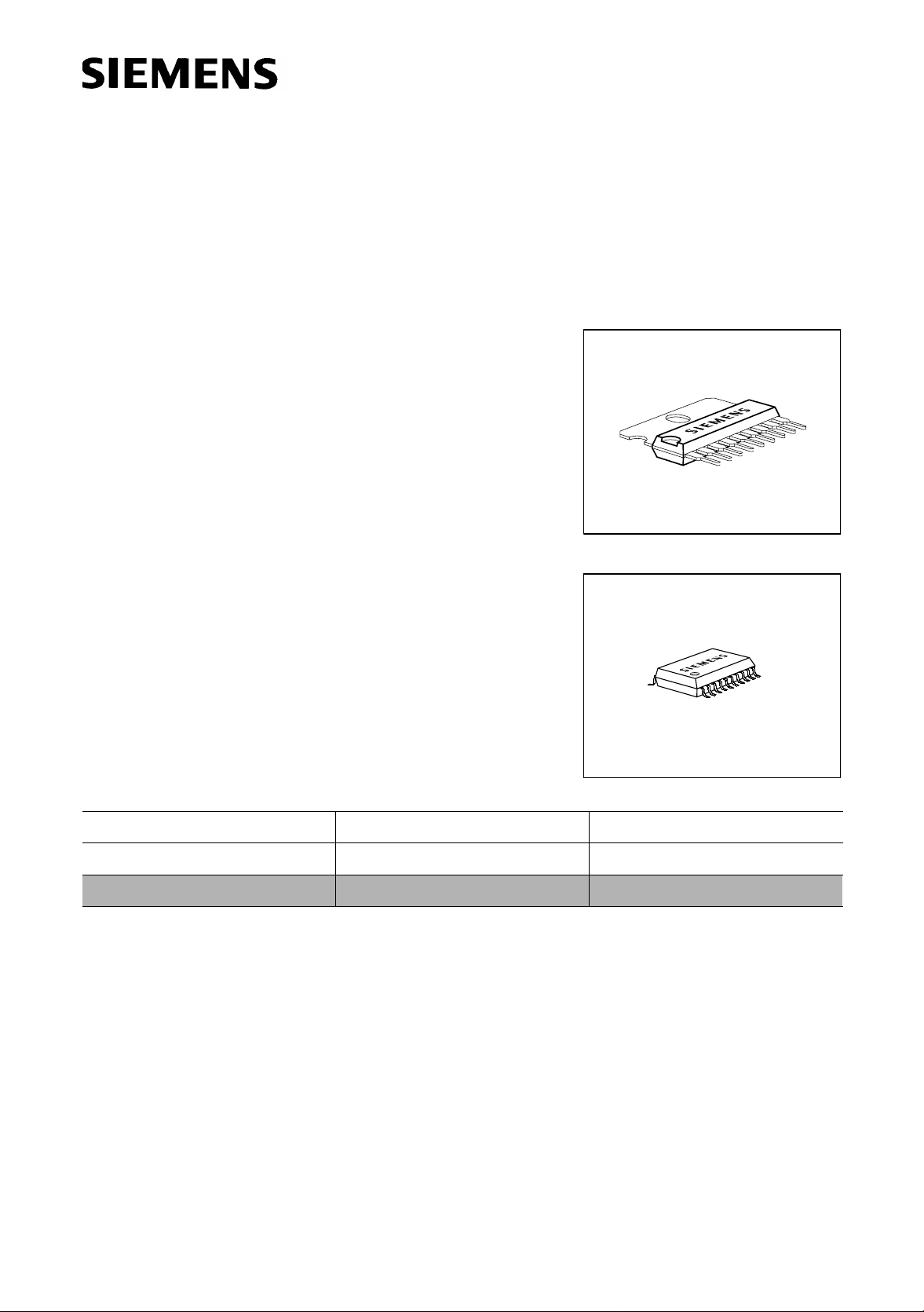
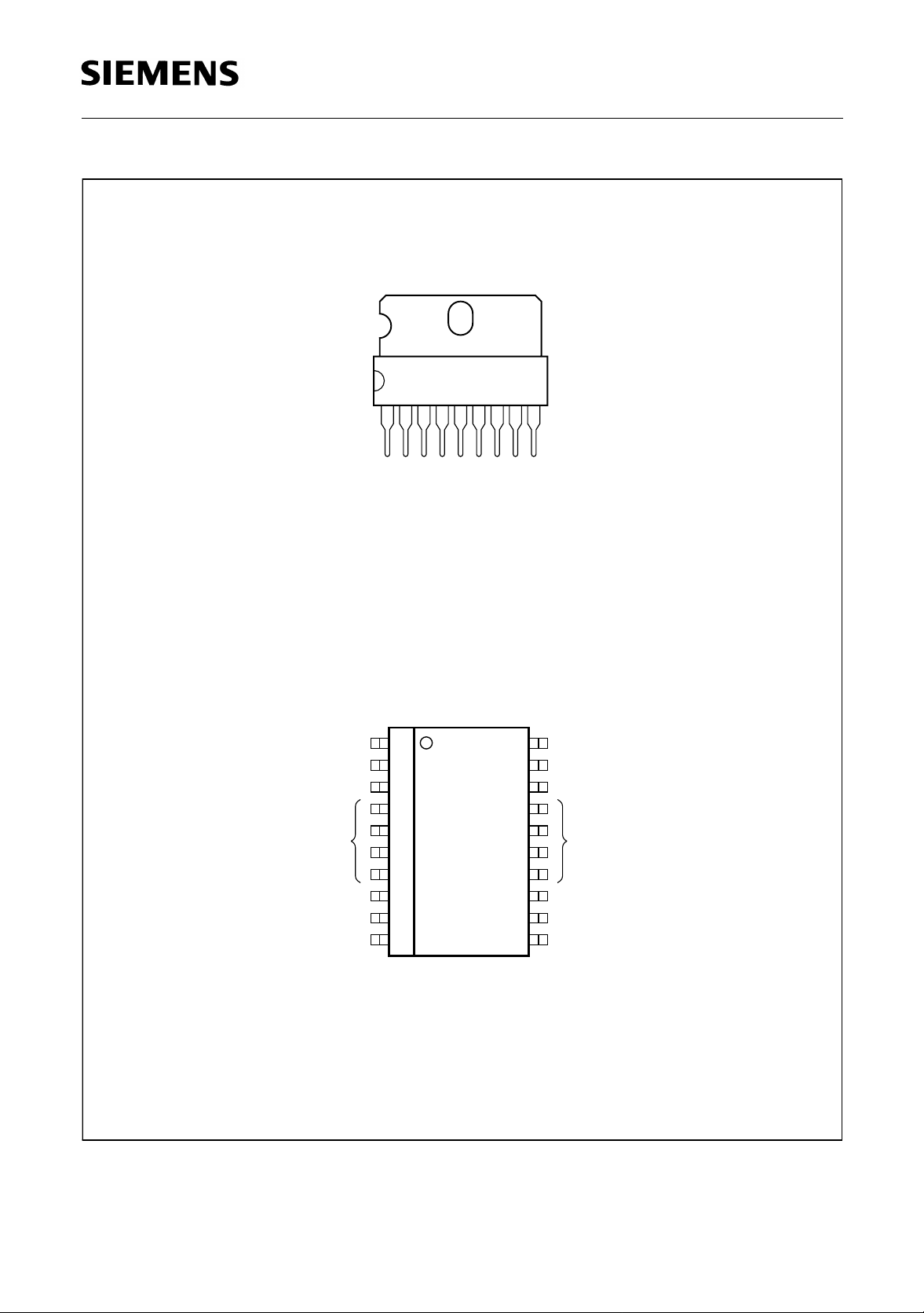
TCA 2465 Q67000-A8109 P-SIP-9-1
TCA 2465 G Q67000-A8334 P-DSO-20-6
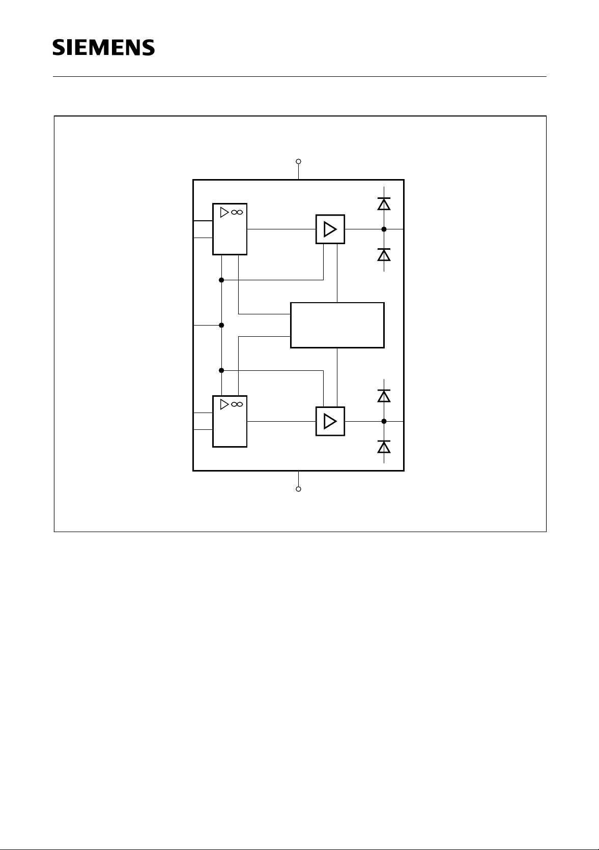
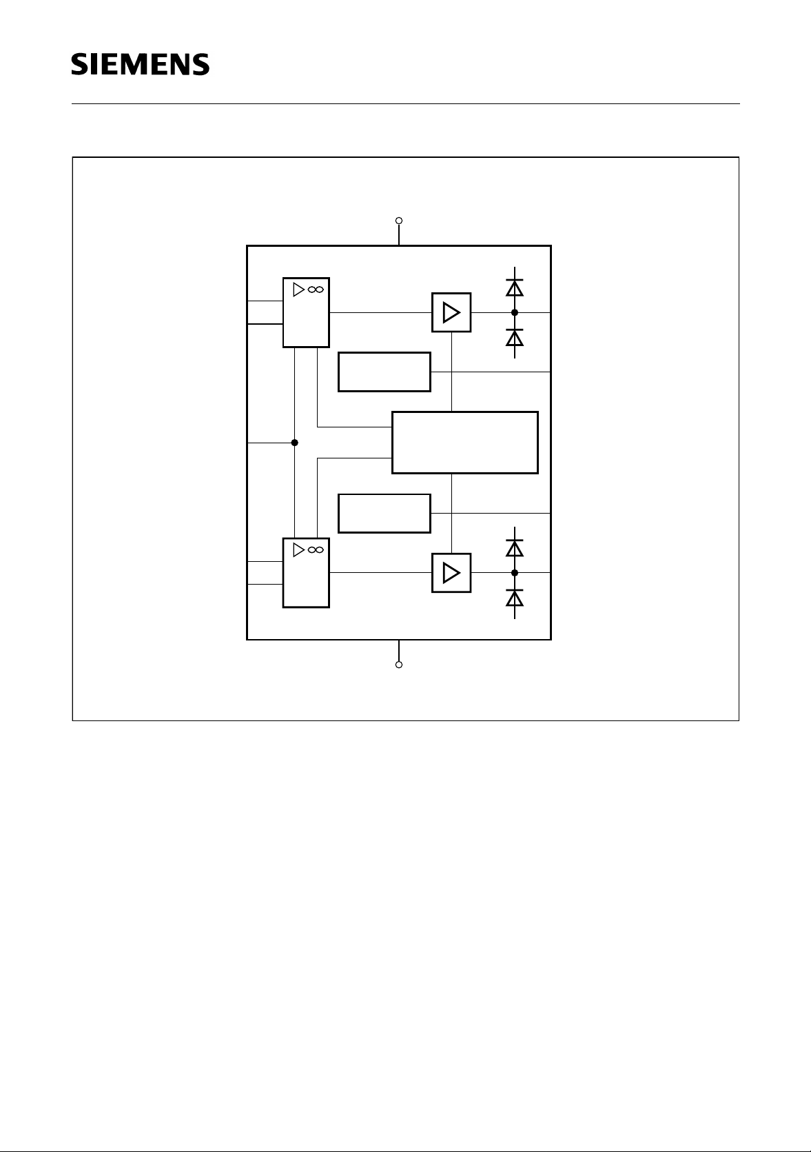
Description
The IC contains two identical op amps , eac h su pply ing a hig h outp ut cu rre nt of 2 .5 A at
supply voltages between ± 3V and
± 20 V. Internal compensation permits negative
feedback of the amplifiers up to a min. of 20 dB. Both amplifiers can be disconnected at
V
≥ 2 V via an inhibit input. Integrated protective circuits protect the outputs against
8
V
short-circuit to +
and – VS and prevent thermal overloading of the IC. TCA 2465 G
S
comes in a special surface -mounted power package si milar to P-DSO-20 and delivers
twice 2.0 A output peak curr ent.
Semiconductor Group 1 1998-02-01
Page 2
TCA 2465
TCA 2465
1
V
+
S
Output 1
N.C.
-
V
S S
Inverting Input 1
Non-Inverting Input 1
Frequency Compensation 1
S
VSV
-
+
-Input 1
+Input 1
Output 1
TCA 2465 G
1
2
3
4
5
6
7
8
9
10
9
-Input 2
+Input 2
Output 2
Inhibit Input
IEP00550
20
19
18
17
16
15
14
13
12
11
Inhibit
Output 2
N.C.
V
-
Inverting Input 2
Non-Inverting Input 2
Frequency Compensation 2
IEP00888
Figure 1 Pin Configuration (top view)
Semiconductor Group 2 1998-02-01
Page 3
TCA 2465
V
+
S
+Input 1
-Input 1
Inhibit
Input
+Input 2
-Input 2
80 dB
5
3
+
2
-
6
TCA 2465
0 dB
Power Limitation
and
1
Output 1
Thermal Protection
7
+
8
-
9
Output 2
0 dB
80 dB
4
IEB00551
Figure 2 Block Diagram TCA 2465
V
-
S
Semiconductor Group 3 1998-02-01
Page 4
TCA 2465
V
+
S
Non-Inverting
Input 1
Inverting
Input 1
Inhibit
Non-Inverting
Input 2
Inverting
Input 2
9
8
20
12
13
80 dB
+
-
TCA 2465 G
+
-
80 dB
1
Frequency
Compensation
Power Limitation
Temperature Protection
Frequency
Compensation
4...7,14...17
0 dB
and
0 dB
2
10
11
19
IEB00889
Output 1
Frequency
Compensation 1
Frequency
Compensation 2
Output 2
Figure 3 Block Diagram TCA 2465 G
V
-
S
Semiconductor Group 4 1998-02-01
Page 5
TCA 2465
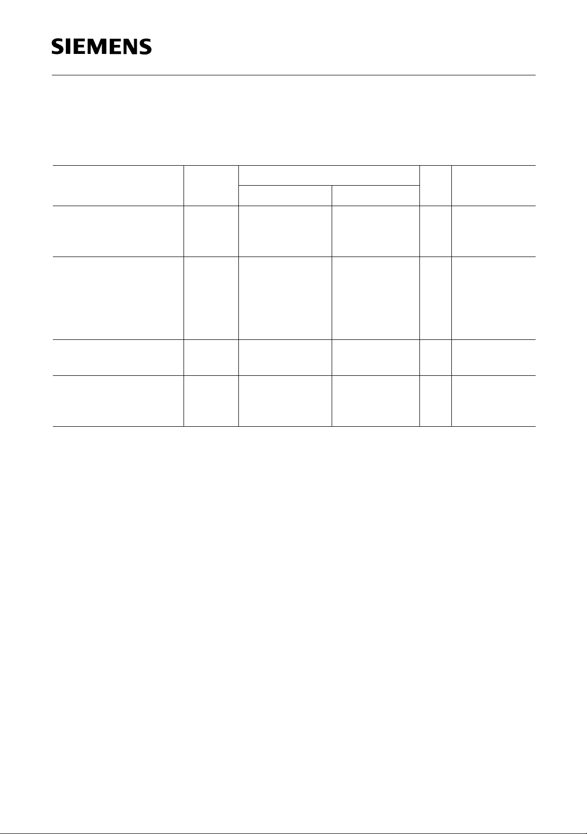
Absolute Maximum Ratings
T
= –40to85°C
C
Note: Values in brackets refer to TCA 2465 G
Parameter Symbol Limit Values Unit Remarks
min. max.
Supply voltage
Differential input
voltage
Output current
Output current
Supply current
Ground current
Input voltage
Inhibit input
Junction temperature
Storage temperature
range
1)
t <1ms, f ≤ 400 Hz
V
S
V
ID
I
Q
I
Q
I
S
I
GND
V
I
V
6
T
j
T
stg
–
–
–2.5(–2)
–1.5
–5(–2)
1)
–5.5(–2)
– V
S
– V
S
–
–50
± 21
V
)+(VS)VV
(–
S
1)
2.5 (2)
–
5.5 (2)
1)
5(2)
V
V
150
1)
A
A
1)
1)
S
S
A
A
V
V
°C°C–
∆
V
or ∆V
2-3
I
or I
1
9
V
≥±15 V;
S
V
<–V
Q
I
S
I
4
V
, V3, V7, V
2
8-7
S
8
150
Semiconductor Group 5 1998-02-01
Page 6
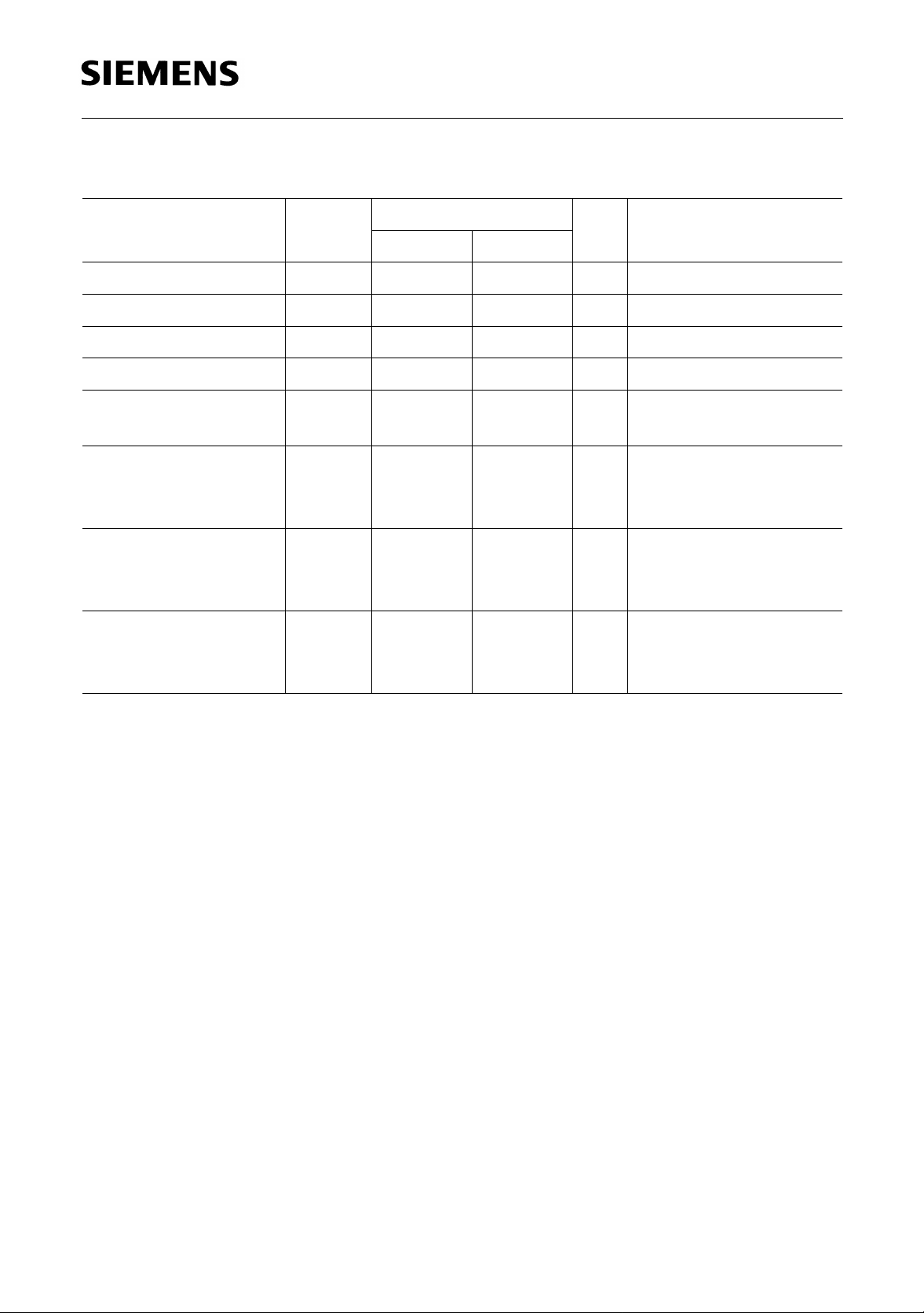
Operating Range
Parameter Symbol Limit Values Unit Remarks
min. max.
TCA 2465
Supply voltage
Output current
Case temperature
V
I
T
Voltage gain G
Forward current
of
F
I
I
free wheeling diodes
Thermal resistance
junction - ambient
junction - case
R
R
Thermal resistance
junction - ambient
junction - case
R
R
Thermal resistance
junction - ambient
junction - case
1)
P
= 12 W P-SIP-9-1
D
P
= 3.5 W P-DSO-20-6
D
R
R
S
Q
C
Vmin
F
th jA
th jC
th jA
th jC
th jA
th jC
± 3 ± 20 V –
(– 1.3) (1.3) A –
– 40 85 °C
1)
20 – dB –
–(1.3)A–
–
–
–
–
–
–
60
5
60
12
(70)
(22)
K/W
K/W
K/W
K/W
K/W
K/W
P-SIP-9-1
P-SIP-9-1
P-DIP-16-2
P-DIP-16-2
(soldered) P-DSO-20-6
P-DSO-20-6
Semiconductor Group 6 1998-02-01
Page 7
TCA 2465
Characteristics
V
= ± 10 V; Tj=25°C, unless otherwise specified
S
Note: Values in brackets refer to TCA 2465; G
Parameter Symbol Limit Values Unit Test
Circuit
1; 12
Open-loop supply current
consumption S1 in position 1
S1 in position 2
min. typ. max.
I
S
I
S
–
–
–
30
5
50
mAmA1; 12
Input offset voltage
Input offset current
Input current
Output volt age
R
=12Ω; f =1kHz
L
R
=4Ω; f =1kHz
L
R
= 470 Ω; f =40kHz
L
1)
Input resistance
f =1kHz
Open-loop voltage gain
f = 100 kHz
Common-mode input voltage
range
Common-mode rejection
Supply voltage rejection
Temperature coefficient of
–40°C ≤ Tj≤ +85°C
Temperature coefficient of
–40°C ≤ Tj≤ +85°C
V
I
IO
IO
V
I
I
V
V
V
R
G
V
k
k
α
α
IO
IO
I
Q pp
Q pp
Q pp
I
VO
IC
CMR
SVR
VIO
IIO
– 10 – 10 mV 2; 13
–100
–
± 8.5
± 8
–
–
0.25
± 9
± 8.5
± 8
1001nA
µA
–
–
–
V
V
V
3; 14
3; 14
4; 15
4; 15
4; 15
15 –MΩ 4; 15
70 80 – dB 5; 16
7/– 10 ± 7.5/– 10.5 – V 6; 17
70
–70
–
–
80
–80
50
0.4
–
–
–
–
dB
dB
µV/K
nA/K
6; 17
7; 18
2; 13
3; 14
Slew rate of
Q
for
SR
–
2(0.5)
–
V/µs
8; 19
V
non-inverting operation
V
Slew rate of
Q
for
SR
–
2(0.5)
–
V/µs
9; 20
inverting operation
Noise voltage
V
n
–3 –µV1;12
(DIN 45405, referred to input)
Inhibit input
V
(referred to –
V
for IC turned OFF
6
V
for IC turned ON
6
Semiconductor Group 7 1998-02-01
)
S
V
V
6 OFF
6 ON
2
–
–
–
–
0.8VV
1; 12
1; 12
Page 8
TCA 2465
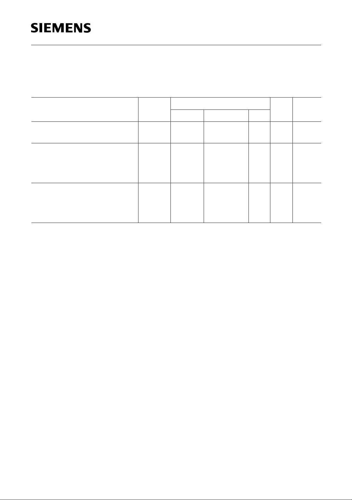
Characteristics (cont’d)
V
= ± 10 V; Tj=25°C, unless otherwise specified
S
Note: Values in brackets refer to TCA 2465; G
Parameter Symbol Limit Values Unit Test
Circuit
1; 12
1; 12
H-input current, V6=5V
L-input current, V6=0V
min. typ. max.
2)
2)
I
6H
I
6
–
–
0.1
0.5
0.53µA
µA
Turn-ON dead time
I>A
3)
I
I
1; 9
Turn-OFF dead time
I I
1; 9
I<1A
3)
Short-circuit current
referred to
V
6 OFF/ON
4)
(switch S3 closed)
Short-circuit current
4)
(switch S4 closed)
1)
Only for P-SIP-9-1
2)
Referred to – V
3)
Switch S2 closed
4)
Only for P-SIP-9-1, for P-DSO-20-6 VS≤±7V
S
t
D ON
t
D OFF
I
SC
I
SC
–
–
–
–
10
10
1
1
20
20
–
–
µs
µs
A
A
1; 12
1; 12
1; 12
1; 12
Semiconductor Group 8 1998-02-01
Page 9

Test Circuits
12, 9
20
13, 8
TCA 2465
V
+
S
11, 10
1
+
-
19, 2
4
Ω100 k
Ω1
4Ω
10 kΩ
10 kΩ
V
-
S
220 nF
S1
IES01367
Figure 4 Open-Loop Supply Current Consumption; Noise Voltage (TCA 2465 G)
+
V
S
11, 10
+
V
-
20
Ω4.7 k
Q
Ω1
V
= 100
Q
V
OΙ
47 Ω
-
V
S
47 Ω
Figure 5 Input Offset Voltage; Temperature Coefficient of
Semiconductor Group 9 1998-02-01
220 nF
IES01368
V
(TCA 24 65 G)
IO
Page 10

TCA 2465
+
V
S
S1
1 MΩ
(220 pF)
11, 10
-
V
+
Q
S2
1 MΩ
20
Ω1
4.7 kΩ
+
=
Ω100
47 Ω
V
-
S
220 nF
IES01369
Figure 6 Input Offset Current; Input Current; Temperature Coefficient of IIO
(TCA 2465 G)
+
V
S
S
µ
10 F
V
Ι
1MΩ
+
-
11, 10
V
Q
20
42.3 kΩ
Ω1
R
L
4.7 kΩ
Ω4.7 k
V
-
S
220 nF
IES01370
Figure 7 Output Voltage; Input Resistance (TCA 2465 G)
Semiconductor Group 10 1998-02-01
Page 11

~
~
= 100 Hz
f
=
10 kΩ
TCA 2465
+
V
S
= 20 x log (101 x /(
G
V0
V
Ι
10 kΩ
11, 10
-
100 Ω
Ω10 k
+
20
Ω10
Ω100 k
Ω1
220 nF
8.2 Ω
V
V
((
Q
Ι
V
Q
-
V
S
Figure 8 Open-Loop Voltage Gain GVO (TCA 2465 G)
+
V
S
11, 10
20
S
=
100 Ω
Ω4.7 k
Ω10
~
= 100 Hz
f
~
-
+
-
V
Ω1
220 nF
IES01371
8.2 Ω
IES01372
V
Q
Figure 9 Common Mode Voltage Gain
G
VC
Common-Mode Rejection
k
Semiconductor Group 11 1998-02-01
(dB) = GVO(dB) – GVC(dB) (TCA 2465 G)
CMR
Page 12

~
~
f
1000 F
100 Hz=
Ω47
47 Ω
TCA 2465
+
V
S
k
(dB) = 20 x log ∆
SVR
Ω56
µ
∆
V
S
-
+
220 nF
470 Ω
11, 10
V
(/(
G
x
Q
V
V
Q
∆
V
((
S
-
V
S
Figure 10 Supply Voltage Rejection k
+
V
S
11, 10
+
-
20
20
(TCA 2465 G)
SVR
(220 pF)
Ω1
220 nF
Ω91 k
Ω1
8.2 Ω
IES01373
V
Q
8.2 Ω10 kΩ
Square-Wave
~
(Peak-to-Peak)
~
0.6 V
10 kΩ
-
V
S
220 nF
IES01374
Figure 11 Slew Rate for Non-Inverting Operation (TCA 2465 G)
Semiconductor Group 12 1998-02-01
Page 13

+
V
S
Ω10 k 100 kΩ
(220 pF)
11, 10
TCA 2465
Square-Wave
~
(Peak-to-
~
Peak) 0.6 V
+
20
Ω10 k
-
V
S
Ω1
220 nF
Figure 12 Slew Rate for Inverting Operation (TCA 2465 G)
8.2 Ω
IES01375
V
Q
Semiconductor Group 13 1998-02-01
Page 14

a) Amplifier; GV=5
TCA 2465
12, 9
13, 8
4.7 kΩ
~
~
b) Voltage follower TCA 2465 G
+ 10 V
1
+
-
4
- 10 V
+ 10 V
11, 10
19, 2
20
220 pF
(220 pF)
5.6 kΩ
Ω22 k
Ω1
220 nF
12 Ω
IES01376
11, 10
1
12, 9
~
~
13, 8
+
4
- 10 V
19, 2
20
Figure 13 Non-Inverting Operation (TCA 2465 G)
Ω1
220 nF
12 Ω
IES01377
Semiconductor Group 14 1998-02-01
Page 15

a) Amplifier; GV=–5
TCA 2465
+ 10 V
1 11, 10
Ω12 k
12, 9
13, 8
+
-
19, 2
15 kΩ
~
~
b) Inverter TCA 2465 G
10 kΩ
12, 9
13, 8
420
- 10 V
+ 10 V10 V
1 11, 10
+
-
420
Ω75 k
220 pF
19, 2
Ω10 k
Ω1
220 nF
Ω1
220 nF
12 Ω
IES01378
12 Ω
~
~
- 10 V
IES01379
Figure 14 Inverting Operation (TCA 2465 G)
Semiconductor Group 15 1998-02-01
Page 16

TCA 2465
V
+
S
5
3, 7
2, 8
+
6
1, 9
4
Ω100 k
10 kΩ
V
-
S
Ω1
220 nF
S1
1
2
10 kΩ
S3
4Ω
S4 S2
IES00553
Figure 15 Open-Loop Supply Current Consumption; Noise Voltage (TCA 2465/A)
+
V
S
+
V
Ω1
220 nF
Q
V
Q
47 Ω
6
Ω4.7 k
47 Ω
-
V
S
Figure 16 Input Offset Voltage; Temperature Coefficient of
= 100
V
OΙ
IES00554
V
(TCA 2465/A)
IO
Semiconductor Group 16 1998-02-01
Page 17

TCA 2465
+
V
S
S1
1 MΩ
-
V
+
Q
S2
1 MΩ
6
Ω1
4.7 kΩ
+
=
Ω100
47 Ω
V
-
S
220 nF
IES00555
Figure 17 Input Offset Current; Input Current; Temperature Coefficient of IIO
(TCA 2465)
+
V
S
S
µ
10 F
V
Ι
1MΩ
+
V
-
Q
6
42.3 Ωk
Ω1
R
L
4.7 Ωk
kΩ4.7
V
-
S
220 nF
IES00556
Figure 18 Output Voltage; Input Resistance (TCA 2465)
Semiconductor Group 17 1998-02-01
Page 18

~
~
= 100 Hz
f
10 kΩ
TCA 2465
+
V
S
= 20 x log ( /(
G
V0
V
Ι
10 kΩ
-
100 Ω
Ω10 k
+
6
Ω100 k
Ω1
8.2 Ω
101
V
V
x
V
((
Q
Ι
Q
=
Ω10
-
V
S
Figure 19 Open-Loop Voltage Gain GVO (TCA 2465)
+
V
S
=
100 Ω
Ω4.7 k
Ω10
~
= 100 Hz
f
~
-
+
6
220 nF
Ω1
220 nF
IES00557
8.2 Ω
V
Q
IES00558
Figure 20 Common Mode Voltage Gain
Common-Mode Rejection k
CMR
-
V
S
G
VC
(dB) = GVO(dB) – GVC(dB) (TCA 2465/A)
Semiconductor Group 18 1998-02-01
Page 19

~
~
1000 F
= 100 Hz
f
TCA 2465
+
V
S
k
(dB) = 20 x log ∆
SVR
Ω56
µ
∆
V
S
220 nF
470 Ω
V
(/(
G
x
Q
V
∆
V
((
S
Ω47
47 Ω
-
+
-
V
S
Figure 21 Supply Voltage Rejection k
+
V
S
+
-
6
(TCA 2465)
SVR
Ω1
220 nF
8.2 Ω
IES00559
V
Q
V
Q
Square-Wave
~
(Peak-to-Peak)
~
0.6 V
6
-
V
S
Ω91 k
10 kΩ
Ω1
220 nF
8.2 Ω10 kΩ
IES00560
Figure 22 Slew Rate for Non-Inverting Operation (TCA 2465)
Semiconductor Group 19 1998-02-01
Page 20

+
V
S
Ω10 k 100 kΩ
TCA 2465
Square-Wave
~
(Peak-to-
~
Peak) 0.6 V
+
6
Ω10 k
-
V
S
Ω1
220 nF
Figure 23 Slew Rate for Inverting Operation (TCA 2465)
Note: Values in brackets refer to TCA 2465 A
Amplifier; GV=5
+10 V
5
8.2 Ω
IES00561
V
Q
3, 7
~
~
4.7 kΩ
2, 8
+
-
-10 V
1, 9
64
Ω22 k
5.6 kΩ
Ω1
220 nF
4Ω
IES00562
Figure 24 Non-Inverting Operation (TCA 2465)
Semiconductor Group 20 1998-02-01
Page 21

Amplifier; GV=–5
TCA 2465
+10 V
5
Ω12 k
3, 7
2, 8
+
-
1, 9
46
15 kΩ
~
~
-10 V
Figure 25 Inverting Operation (TCA 2465)
Ω1
Ω75 k
220 nF
4Ω
IES00564
Semiconductor Group 21 1998-02-01
Page 22

TCA 2465
Safe Operating Area (SOA) Peak Output
Current versus Collector-Emitter Voltage
T
=25°C, VCE=+VS– VQor VCE=–VS– V
j
4.0
A
Ι
Q
3.5
3.0
2.5
2.0
1.5
1.0
0.5
0
10 20 30 40 V 50
0
IED00576
V
CE
Max. Permissible Power Dissipation versus
Case Temperature
Q
24
W
P
tot
20
16
12
8
4
0
0
TCA 2465G
25 50
TCA 2465
75 100 ˚C 150
IED00566
T
C
Supply Current versus
T
Supply Voltage
50
Ι
S
mA
40
30
20
10
0
0
5 10 15 20 V 25
=25°C
j
IED00567
V
S
Input Current versus
Junction Temperature
300
Ι
Ι
nA
250
200
150
100
-40
-25 0 25 50 75
V
= ± 10 V
S
IED00568
˚C
T
j
Semiconductor Group 22 1996-05-01
Page 23

TCA 2465
Open-Loop Voltage Gain versus
Frequency
100
G
VO
dB
80
V
= ±10 V
S
T
j
25= ˚C
70
60
50
40
30
20
10
0
10
1
10
2
10
3
10410
IED00569
5
Hz
f
10
Phase Response versus Frequency
V
= ± 10 V; Tj=25°C
S
0
Deg.
-
Φ
-30
-60
-90
-120
-150
6
-180
1
2
10310410510610710Hz
10
IED00570
f
TCA 2465, G Open-Loop Voltage Gain
versus Frequency
V
= ± 10 V, Tj=25°C
S
100
G
VO
dB
80
C
comp
C
C
comp
comp
70
60
50
40
30
20
10
IED00571
= 220 pF
= 100 pF
= 0 pF
TCA 2465, G Phase Response
versus Frequency
V
= ± 10 V, Tj=25°C
S
0
Deg.
-
Φ
-30
-60
-90
-120
-150
IED00570
0
10
1
10210
3
10410510
Hz
f
6
-180
1
2
10310410510610710Hz
10
f
Semiconductor Group 23 1996-05-01
Page 24

TCA 2465
Common-Mode Rejection versus
Case Temperature
V
= ± 10 V
S
IED00573
k
CMR
90
dB
85
80
75
Saturation Voltage versus
Peak Output Current
T
=25°C
j
2.0
V
Sat
V
1.5
1.0
0.5
= 25 ˚C
T
j
TCA 2465G
TCA 2465
IED00574
70
-25 0 25 50 75
-40
Forward Current versus
Forward Voltage
3.0
Ι
F
A
2.0
1.0
Pins 1, 9
Pin 4
TCA 2465
˚C
T
C
IED00575
= 25 ˚C
T
j
TCA 2465G
0
0
0.5 1.0 1.5 2.0 A 2.5
Ι
Q
Pin (9) 5
Pins (7, 10) 1, 9
0
0
1.0 V 2.0
V
F
Semiconductor Group 24 1996-05-01
Page 25

Package Outlines
P-SIP-9-1
(Plastic Single In-line Package)
TCA 2465
Sorts of Packing
Package outlines for tubes, trays etc. are contained in our
Data Book “Package Information”.
GPI05038
Dimensions in mm
Semiconductor Group 25 1998-02-01
Page 26

P-DSO-20-6
(Plastic Dual Small Outline Package)
1.27
+0.15
0.35
2)
0.2 24x
1120
-0.1
0.2
-0.2
2.45
0.1
7.6
2.65 max
10.3
0.35 x 45˚
1)
-0.2
+0.8
0.4
±0.3
GPS05094
+0.09
0.23
TCA 2465
8˚ max
110
12.8
-0.2
1)
Index Marking
1) Does not include plastic or metal protrusions of 0.15 max per side
2) Does not include dambar protrusion of 0.05 max per side
Sorts of Packing
Package outlines for tubes, trays etc. are contained in our
Data Book “Package Information”.
SMD = Surface Mounted Device
Dimensions in mm
Semiconductor Group 26 1998-02-01
 Loading...