

Datasheet TC96C555EOA, TC96C555EPA, TC96C555CPA, TC96C555COA, TC96C555MJA Datasheet (TelCom Semiconductor)
Page 1
3A OUTPUT PROGRAMMABLE POWER OSCILLATOR
1
TC96C55
FEATURES
■ Controllable Duty Cycle
■ Wide Operating Range .............................5V to 18V
■ High Peak Output Current .................................. 3A
■ High Capacitive Load Drive
Capability .................................... 1800pF in 20nsec
■ Short Delay Time ............................. < 150nsec Typ
APPLICATIONS
■ Fixed Frequency Power Oscillator
■ Voltage Controlled Oscillator
■ Low Power Buck Regulator Supply
■ MOSFET Driver
■ Simple diode inverters and doublers
ORDERING INFORMATION
Operating
Part No. Package Temp Range
TC96C555COA 8-Pin SOIC 0°C to +70°C
TC96C555CPA 8-Pin Plastic DIP 0°C to +70°C
TC96C555EOA 8-Pin SOIC – 40°C to +85°C
TC96C555EPA 8-Pin Plastic DIP – 40°C to +85°C
TC96C555MJA 8-Pin CerDIP – 55°C to +125°C
GENERAL DESCRIPTION
The TC96C555 Power Oscillator is an easily programmed IC that can be used in simple switch-mode power
supplies, diode doublers and inverters, and similar circuits
where high-current pulses are needed in an economical
form.
The TC96C555 uses TelCom Semiconductors' new
Tough CMOS™ process. The output drive capability is
similar to the TC4423/4/5 MOSFET Drivers, which can
switch in 25nsec into a capacitive load of 1,800pF. The
TC96C555 will not latch up under any conditions within their
power and voltage ratings. They can accept, without damage, up to 1.5A of reverse current (of either polarity) being
forced back into the output. All terminals are also fully
protected against up to 4kV of electrostatic discharge. The
peak output is rated at 3A. Split outputs permits driving of an
external pair of MOSFETS, with controllable cross conduction between upper and lower devices.
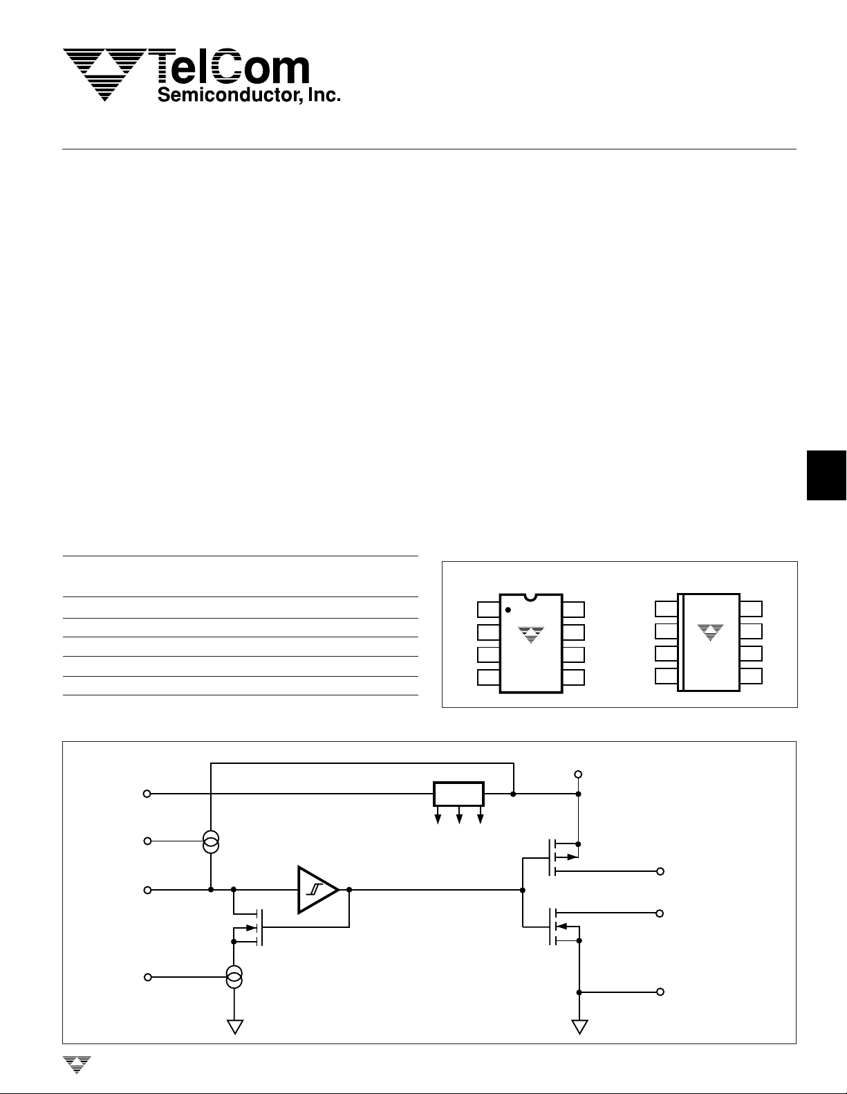
PIN CONFIGURATIONS (DIP and SOIC)
V
V
V
18
R2
27
V
IN
TC96C555CPA
36
REF
V
R1
TC96C555EPA
45
R2
GND
OUT
OUT
V
DD
18
V
IN
2
V
REF
36
V
R1
45
TC96C555COA
TC96C555EOA
GND
7
OUT
OUT
V
DD
2
3
4
5
FUNCTIONAL BLOCK DIAGRAM
V
REF
3
4
V
R1
V
IN
V
R2
3V
2
1
3V
I
SOURCE
I
SINK
TELCOM SEMICONDUCTOR, INC.
V
DD
+4V
2V
1V
Q
3
V
REF
1V 2V 3V
8
Q
1
7
OUTPUT A
OUTPUT B
Q
2
6
GND
5
6
7
8
TC96C555-7 10/21/96
4-159
Page 2

TC96C555
3A OUTPUT PROGRAMMABLE
POWER OSCILLA TOR
ABSOLUTE MAXIMUM RATINGS
Supply Voltage ......................................................... +20V
Input Voltage, Pin 1 or 4.................V
Maximum Chip Temperature.................................+150°C
Storage Temperature Range ................– 65°C to +150°C
Package Thermal Resistance
CerDIP R
CerDIP R
PDIP R
PDIP R
................................................................ 150°C/W
ΘJ-A
...................................................................50°C/W
ΘJ-C
.................................................................... 125°C/W
ΘJ-A
.......................................................................42°C/W
ΘJ-C
+0.3 to GND –0.3
DD
SOIC R
SOIC R
Operating Temperature Range
C Version...............................................0°C to +70°C
E Version ..........................................– 40°C to +85°C
M Version .......................................– 55°C to +125°C
Package Power Dissipation (TA ≤ 70°C)
Plastic DIP ......................................................730mW
CerDIP............................................................800mW
SOIC...............................................................470mW
ELECTRICAL CHARACTERISTICS: unless otherwise specified T
.................................................................... 155°C/W
ΘJ-A
.......................................................................45°C/W
ΘJ-C
= +25°C with 5V ≤ VDD ≤ 18V.
A
Symbol Parameter Test Condition Min Typ Max Unit
Programmable Current Range
Pin 4 Input Current for I
Pin 1 Input Current for I
Control (V
SOURCE
Control (V
SINK
REF
REF
- VR1) / R
- VR2) / R
CHG
Fig. 2
DIS
Fig. 2
5.0 — 150 µA
5.0 — 150 µA
Reference Section
V
REF
V
DRIFT
TCV
V
R1, VR2
V
REF
V
ih
V
il
V
ih
I
REF
REF
- V
- V
Line Regulation of V
Load Regulation of V
V
Drift Over Lifetime — — 5 %
REF
V
Tempco
REF
Voltage at Pin 1 & 4 2.85 3.0 3.15 V
R
Voltage Across R
Pin 2, High Switching Threshold
Pin 2, Low Switching Threshold
il
Delta High to Low Threshold
V
Pin 3 Short to GND Pin 5
REF
CHG
REF
REF
and R
DIS
ELECTRICAL CHARACTERISTICS: unless otherwise specified T
VDD = 15V, I
REF
= 10µA
3.8 4 4.2 V
VDD = 7V to 18V — 0.6 1 %/V
I
= 0 to 1mA — 0.1 0.2 %/mA
REF
– 55 ≤ Temp ≤ 125°C
— 1100 2000 ppm/°C
0.85 1 1.15 V
VDD = 15V 1.8 2 2.2 V
VDD = 15V 0.8 1 1.2 V
VDD = 15V 0.9 1.0 1.1 V
VDD = 15V — 8 15 mA
= +25°C with 10V ≤ V
A
DD
≤ 18V:
Symbol Parameter Test Condition Min Typ Max Unit
Oscillator
Voltage Stability VDD = 7 to 18V – 1 5 %/V
Temperature Stability – 55 ≤ Temp ≤ 125°C – 0.4 – %/°C
Power Supply
Power Supply Current IDD0 ≤ VIN ≤ 3V – 2 3 mA
Switching Time
t
R
t
F
t
D1
t
D2
1
Rise Time C1 = 1800pF – 23 30 nsec
Fall Time C1 = 1800pF – 20 30 nsec
Delay Time C1 = 1800pF – 140 180 nsec
Delay Time C1 = 1800pF – 100 140 nsec
Output
V
OH
V
OL
R
O
R
O
I
PK
4-160
High Output Voltage
V
DD
– 0.025
–– V
Low Output Voltage – – 0.025 V
Output Res Hi State VDD = 15V – 3.5 5 Ω
Output Res Lo State V
= 15V – 2.5 5 Ω
DD
Peak Output Current VDD = 18V – 3 – A
TELCOM SEMICONDUCTOR, INC.
Page 3
3A OUTPUT PROGRAMMABLE
POWER OSCILLA TOR
TC96C555
ELECTRICAL CHARACTERISTICS: specifications over operating temperature range unless otherwise
specified 5.0V < V
Symbol Parameter Test Condition Min Typ Max Unit
Programmable Current Range
Pin 4 Input Current for I
Pin 1 Input Current for I
Control (V
SOURCE
Control (V
SINK
REF-VR1
REF-VR2
Reference Section
V
REF
VDD = 7 to 18V Line Regulation of V
I
= 0 to 1mA Load Regulation of V
REF
V
DRIFT
TCV
REF
V
R1, VR2
V
REF-VR
V
ih
V
il
V
to V
ih
il
I
REF
VDD = 15V I
REF
REF
V
Drift Over Lifetime – – 5 %
REF
V
Tempco – 55 ≤ Temp ≤ 125°C – 1100 2000 ppm/°C
REF
Voltage Pin at 1 and 4 VDD = 15V 2.7 3 3.3 V
Voltage Across R
Pin 2, High Switching Threshold VDD = 15V 1.75 2 2.25 V
Pin 2, Low Switching Threshold VDD = 15V 0.75 1 1.25 V
Delta High to Low Threshold VDD = 15V 0.9 1.0 1.1 V
V
Pin 3 Short to GND Pin 5 VDD = 15V – – 18 mA
REF
CHG
and R
DIS
= 10µA 3.6 4 4.4 V
REF
Oscillator
Voltage Stability VDD = 7V to 18V – 1 8 %/V
Temperature Stability – 55 ≤ Temp ≤ 125°C – 0.4 – %/°C
Power Supply
I
DD
Switching Time
t
R
t
F
t
D1
t
D2
Power Supply Current 0 ≤ VIN ≤ 3V – – 4 mA
1
Rise Time C1 = 180pF, Fig. 1 – 33 40 nsec
Fall Time C1 = 1800pF, Fig. 1 – 30 40 nsec
Delay Time Fg. 1 – 180 220 nsec
Delay Time Fig. 1 – 160 200 nsec
Output
V
OH
V
OL
R
O
R
O
I
PK
NOTE :1Switching times guaranteed by design.
The typical values are from 125°C measurements.
Static-sensitive device. Unused devices must be stored in conductive material. Protect devices from static discharge and static fields. Stresses above those
listed under Absolute Maximum Ratings may cause permanent damage to the device. These are stress ratings only and functional operation of the device
at these or any other conditions above those indicated in the Operational Specifications is not implied. Any exposure to Absolute Maximum Rating
Conditions may affect device reliability.
High Output Voltage
Low Output Voltage – – 0.025 V
Output Res Hi State V
Output Res Lo State VDD = 15V – 3.4 6 Ω
Peak Output Current VDD = 18V – 2 – A
= 15V – 4.5 6 Ω
DD
DD
) / R
) / R
<18V.
Fig. 2
CHG
Fig. 2
DIS
5.0 – 100 µA
5.0 – 100 µA
– 0.9 1.5 %/V
– 0.1 0.4 %/mA
0.8 1 1.2 V
V
– 0.025
DD
–– V
1
2
3
4
5
6
7
TELCOM SEMICONDUCTOR, INC.
8
4-161
Page 4

TC96C555
TYPICAL CHARACTERISTICS
3A OUTPUT PROGRAMMABLE
POWER OSCILLA TOR
Fall Time vs. Capacitive Load
VDD = 5V, 10V, 18V
500
Freq = 55KHz
Temp = 25
400
300
200
Fall Time (nsec)
100
0
100 1000 10,000
°
C
C (pF)
LOAD
Rise Time vs. Temperature
60
50
40
VDD = 5V, 10V, 15V
V
= 0 – 5V
IN
C
= 1000pF
LOAD
5V
10V
18V
20,000
Rise TIme vs. Capacitive Load
500
Freq = 55KHz
Temp = 25°C
400
300
200
Rise Time (nsec)
100
0
100 1000 10,000
VDD = 5V, 10V, 18V
C (pF)
LOAD
Fall Time vs. Temperature
60
50
40
VDD = 5V, 10V, 15V
V
= 0 – 5V
IN
C
= 1000pF
LOAD
5V
10V
18V
20,000
5V
30
Rise Tme (nsec)
10V
20
15V
10
–55 –35 5 25 45 65 85 105 125–15
Temperature (°C)
Delay Time vs. Supply Voltage
140
TD1
Temp = –55°C
120
TD2
100
80
60
Delay Time (nsec)
40
V
= 0 – 5V
20
IN
C
= 1000pF
LOAD
0
4681012
Supply Voltage
14 16 18
30
Fall Time (nsec)
5V
20
15V
10
–55 –35 5 25 45 65 85 105 125–15
10V
Temperature (°C)
Delay Time vs. Supply Voltage
Temp = 25°C
350
300
250
200
TD1
150
Delay Time (nsec)
TD2
100
V
= 0 – 5V
50
IN
C
= 1000pF
LOAD
0
4681012
Supply Voltage
14 16 18
4-162
TELCOM SEMICONDUCTOR, INC.
Page 5

3A OUTPUT PROGRAMMABLE
POWER OSCILLA TOR
TYPICAL CHARACTERISTICS (Cont.)
Delay Time vs. Supply Voltage
250
200
TD2
TD1
Temp = 125
°C
250
200
Delay Time vs. Temperature
VDD = 18V
1
TC96C555
2
150
100
Delay Time (nsec)
50
V
= 0 – 5V
IN
C
= 1000pF
LOAD
0
4681012
Supply Voltage
Oscillation Frequency vs. Supply Voltage
Temp at 25°C, – 55°C, 125°C
11.9
125°C
11.7
11.5
25°C
11.3
-55°C
11.1
Frequency (kHz)
10.9
R
= 22K
10.7
DIS
R
= 44K
CHG
C = 1000pF
14 16 18
150
TD1
100
Delay Time (nsec)
Frequency (kHz)
TD2
50
V
= 0 – 5V
IN
C
= 1000pF
LOAD
0
–55 –35 5 25 45 65 85 105 125–15
Temperature (°C)
Oscillation Frequency vs. Temperature
11.9
11.7
11.5
11.3
11.1
10.9
10.7
V
R
C = 1000pF
VS = 5V, 10V, 18V
18V
= 22K
DIS
= 44K
CHG
15V
10V
3
4
5
4681012
Supply Voltage
IDD vs. Supply Voltage
Temp = – 55°C, 25°C, 125°C
3000
2500
2000
–55
°C
(µA)
1500
DD
I
1000
500
0
4681012
25
°C
125
°C
V
= 0V
IN
Supply Voltage
14 16 18
14 16 18
TELCOM SEMICONDUCTOR, INC.
–55 –35 5 25 45 65 85 105 125–15
Temperature (°C)
IDD vs. Supply Voltage
Temp = – 55°C, 25°C, 125°C
3000
2500
2000
–55°C
(µA)
1500
DD
I
1000
500
0
4681012
25
°C
125
°C
V
= 3V
IN
Supply Voltage
6
7
14 16 18
8
4-163
Page 6

TC96C555
TYPICAL CHARACTERISTICS (Cont.)
3A OUTPUT PROGRAMMABLE
POWER OSCILLA TOR
2500
2000
1500
(µA)
DD
1000
I
500
0
–55 –35 5 25 45 65 85 105 125–15
4.2
4.1
4.0
REF
3.9
V
3.8
3.7
IDD vs. Temperature
VDD = 5V, 10V, 15V
15V
10V
5V
V
= 3V
IN
Temperature (°C)
V
vs. Supply Voltage
REF
Temp at 25°C, – 55°C, 125°C
-55°C
25°C
125°C
2000
1500
(µA)
1000
DD
I
500
0
–55 –35 5 25 45 65 85 105 125–15
4.1
4.0
3.9
REF
V
3.8
V
10V
5V
18V
IN
IDD vs. Temperature
VDD = 5V, 10V, 15V
15V
10V
5V
= 0V
Temperature (°C)
V
vs. Temperature
REF
VDD = 5V, 10V, 18V
4-164
4681012
Supply Voltage
R
vs. Supply Voltage
OUT
10
(Ω)
OUT
R
8
6
4
2
0
125
25
–55
V
= 0V
IN
4681012
Output HIGH
°C
°C
°C
Supply Voltage
14 16 18
14 16 18
3.7
–55 –35 5 25 45 65 85 105 125–15
Temperature (°C)
R
vs. Supply Voltage
OUT
Output LOW
7
6
125
°C
5
(Ω)
4
25
OUT
R
°C
3
–55
°C
2
1
V
= 3V
IN
0
4681012
Supply Voltage
TELCOM SEMICONDUCTOR, INC.
14 16 18
Page 7

3A OUTPUT PROGRAMMABLE
POWER OSCILLA TOR
TYPICAL CHARACTERISTICS (Cont.)
R
vs. Temperature
OUT
Output HIGH
Temperature (°C)
(Ohm)
OUT
R
APPLICATIONS
10
8
6
5V
4
10V
2
18V
0
–55 –35 5 25 45 65 85 105 125–15
1
TC96C555
R
vs. Temperature
OUT
7
6
5
4
5V
(Ohm)
3
OUT
10V
R
2
18V
V
= 0V
IN
1
0
–55 –35 5 25 45 65 85 105 125–15
Output LOW
Temperature (°C)
V
= 3V
IN
2
3
The oscillator timing can easily be controlled by two
external resistors, R
and R
set the two constant current sources for charging
DIS
CHG
and R
, and capacitor C. R
DIS
CHG
and discharging C. The source current is always flowing
when in operation. When the capacitor has charged to a 2V
threshold, the current sink circuit is enabled to discharge the
VDD = 18V
TEST CIRCUIT
3
V
REF
4
≤ 10nsec
V
REF
1V 2V 3V
2V
1V
Q
3
2
1
INPUT
100KHz Square Wave
t
= t
RISE
FALL
V
REF
3
R
CHG
4
V
R
DIS
2
V
C
1
V
R2
R1
IN
4V
I
SOURCE
I
SINK
8
TC96C555
GND
5
V
1µF
WIMA
MKS-2
7
6
CERAMIC
C1 = 1800pF
Figure 1. Output Switching Time
DD
8
10µF
Q
1
7
OUTPUT
6
Q
2
GND
5
capacitor to the 1V threshold. When 1V is reached, the
current sink turns OFF to start another cycle.
Resistor R
is connected from V
CHG
at Pin 3 to V
REF
4 to program the charging current. Current is set with resistor
R
connected from V
DIS
Pin 3 to VR2 Pin 1. Both currents
REF
can range from 5µA to 150µA.
0.1µF
OUTPUT
V
IN
OUTPUT
+5V
INPUT
0V
18V
OUTPUT
0V
2V
1V
V
DD
0V
10%
90%
t
D1
t
F
10%
T
CHG
90%
t
D2
t
R
90%
10%
R1
Pin
4
5
6
7
Figure 2. Fixed Frequency Power Oscillator
TELCOM SEMICONDUCTOR, INC.
Figure 3. VIN and Output Waveform
8
4-165
Page 8

TC96C555
APPLICATIONS (Cont.)
Maximum Frequency
R
= 13K, R
CHG
900
700
500
400
300
Frequency in KHz
200
100
100K
10K
100
Frequency in Hz
0.1
Figure 4. Typical Maximum and Minimum
Operating Frequency vs. Capacitor
20 60 8010
Minimum Frequency
R
CHG
1K
10
1
100pF .01µF.1µF10pF
30 50
C in pF
= 200K, R
.001µF
C in pF
= 6.8K
dis
40 100
= 100K
dis
1µF
+12V
3A OUTPUT PROGRAMMABLE
POWER OSCILLA TOR
This circuit will convert a 6 to 15V input to a 5V output of
200 milliamps. Normal operating frequency is 50kHz. Peak
to peak ripple is 50 millivolts. A change from 100mA to
200mA produces a 50mV peak change in V
ery in 200µs.
The TC96C555 is used here as a duty cycle modulator
in a buck output circuit. The source current is modulated to
control the duty cycle. Sink current is fixed at 100µA with a
resistor (R4) of 10K. Transistor Q1, (2N2907A), is used for
current modulation into TC96C555 Pin 4, the charge current
program input. Shunt regulator TL431 is used for voltage
sense and regulation feedback. The TL431 has an internal
reference of 2.495V. Terminal R is compared with this
reference to control conduction of cathode C to anode A. R2
and R3 are selected to give proper bias current to the TL431.
C2 and R7 are for loop compensation and are optimized for
a recovery time of 200µs. The TC96C555 outputs, Pin 7 and
6, are tied together so that when output is HIGH, current
conducts from VDD Pin 8 to output Pin 7 to charge the
inductor, L1. When output is OFF or LOW, energy stored in
L1 will continue to conduct through TC96C555 Pin 6 to the
lower internal MOSFET and out to Pin 5, the ground return.
This circuit does not have current limiting. A fuse is recommended for protection. Figure 6 shows the duty cycle as a
function of the source current. Figure 8 shows the frequency
vs control voltage.
, with recov-
OUT
4-166
L1, 3mH
TL431
C5
100µF
C
C3
100µF
C2
.1µF
100K
R7
R
A
R1
10K
Q1
2N2907A
R2
560Ω
470pF
R4
10K
C6
4.7µF
C1
C4
.1µF
8
V
4
3
1
2
DD
V
R1
V
REF
V
R2
TC96C555
V
IN
GND
7
OUT
OUT
6
5
R3, 390Ω
Figure 5. +5V Buck Regulator Power Supply with 82% Efficiency at 200mA Output
V
OUT
10K
R5
10K
R6
TELCOM SEMICONDUCTOR, INC.
Page 9

3A OUTPUT PROGRAMMABLE
Voltage Controlled Oscillator
R
CHG
= 51k, R
dis
= 25.5k
Frequency in Hz
3.25V 5V
Control Voltage
1000K
100K
10K
1K
100
10
4V 7V
3.5V
0.1
µF
1000pF
100pF
10pF
0.01µF
POWER OSCILLA TOR
1
TC96C555
APPLICATIONS (Cont.)
Duty Cycle vs. Charge Current
100
Duty Cycle in %
16 38 50 1638
80
60
40
20
0
10 30 50 70 90
Figure 6. Duty Cycle vs. Charge Current
Frequency in kHz
20 40 60 80 100
Charge Current in µA
I
SINK
= 100µA
+12V
By connecting both resistors, R
CHG
and R
DIS
, to a
voltage source instead of connecting to the 4V reference of
Pin 3, one can increase or decrease the output frequency.
Increasing the voltage source to 5V will double the oscillator
frequency by doubling the voltage across both R
R
. Decreasing the voltage source to 3.5V will drop the
DIS
CHG
and
frequency in half.
2
3
4
CONTROL
VOLTAGE
SOURCE
8
V
V
V
V
V
REF
R1
IN
R2
DD
TC96C555
GND
3
R
CHG
R
DIS
Figure 7. Voltage Controlled Power Oscillator
C
4
2
1
OUT
OUT
.1µF
Figure 8. Frequency vs Control
7
6
OUTPUT
5
6
7
8
TELCOM SEMICONDUCTOR, INC.
4-167
 Loading...