

Page 1
LOW POWER, BANDGAP VOL T AGE REFERENCES
1
TC9491A
TC9491B
2
FEATURES
■ Temperature Coefficient ......................... 50ppm/°C
■ Wide Operating Current Range .......15µA to 20mA
■ Dynamic Impedance ......................................... 0.6Ω
■ Output Tolerance ...................................... 1% or 2%
■ Output Voltage Option ..................................1.220V
■ TO-92 Plastic Package
■ 8-Pin Plastic Small Outline (SO) Package
APPLICATIONS
■ ADC and DAC Reference
■ Current Source Generation
■ Threshold Detectors
■ Power Supplies
■ Multi-meters
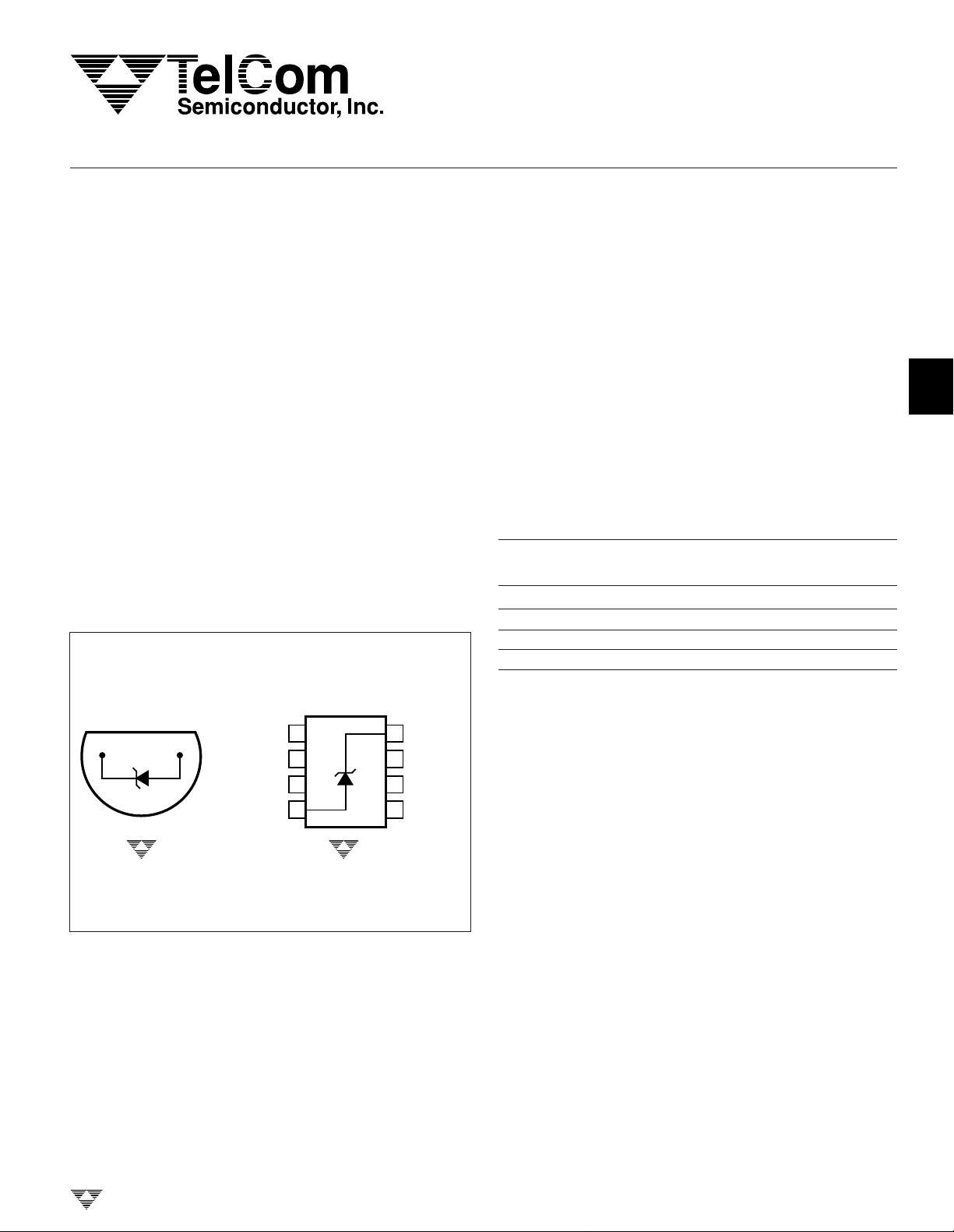
PIN CONFIGURATIONS
TO-92 PLASTIC
(BOTTOM VIEW)
SURFACE MOUNT
PLASTIC PACKAGE
GENERAL DESCRIPTION
The TC9491 (1.220V output) bipolar, two-terminal,
bandgap voltage references offer precision performance
without premium price. These devices do not require thinfilm resistors, greatly lowering manufacturing complexity
and cost.
A 50ppm/°C output temperature coefficient and a 15µA
to 20mA operating current range make these devices attractive for multimeter, data acquisition converter, and telecommunication voltage references.
ORDERING INFORMATION
Part No. Package Temperature Tempco.
Range
TC9491ACOA 8-Pin SOIC 0°C to +70°C 50 ppm°C
TC9491BCOA 8-Pin SOIC 0°C to +70°C 100 ppm°C
TC9491ACZM TO-92 0°C to +70°C 50 ppm°C
TC9491BCZM TO-92 0°C to +70°C 100 ppm°C
3
4
5
1
3
TC9491ACZB
TC94191BCZB
TELCOM SEMICONDUCTOR, INC.
1
NC = NO INTERNAL CONNECTION
NC
NC
NC
ANODE
2
3
4
TC9491ACOA
TC94191BOA
CATHODE
8
NC
7
NC
6
NC
5
6
7
8
TC9491A/B-3 8/23/96
3-15
Page 2
TC9491A
TC9491B
LOW POWER, BANDGAP
VOL T AGE REFERENCES
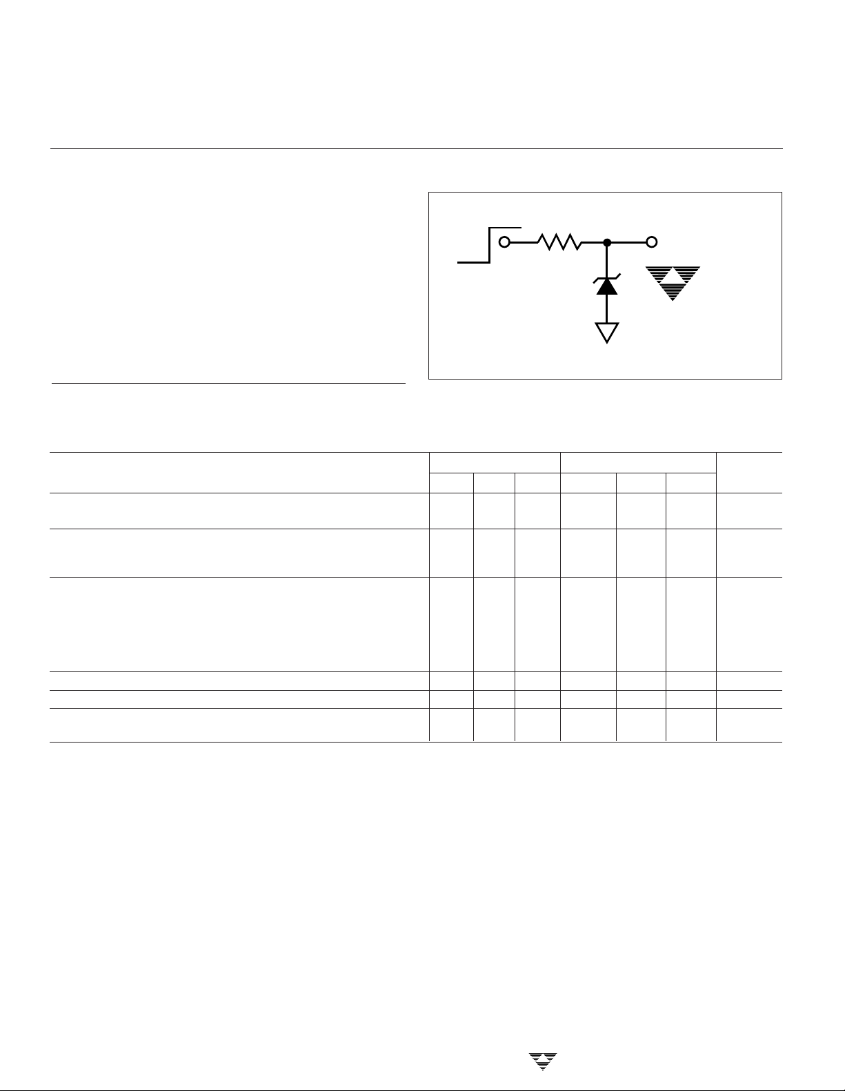
ABSOLUTE MAXIMUM RATINGS*
RESPONSE TIME TEST CIRCUIT
Forward Current .................................................... +10mA
Reverse Current.................................................... +30mA
Storage Temperature Range ................– 65°C to +150°C
Operating Temperature Range
INPUT
36 kΩ
OUTPUT
TO-92 Package ..................................... 0°C to +70°C
COA Surface Mount Package ............... 0°C to +70°C
Lead Temperature (Soldering, 10 sec)
TO-92 Package .............................................. +300°C
TC9491
COA Surface Mount Package ........................ +300°C
Power Dissipation
Limited by Forward/Reverse Current
*Functional operation above the absolute maximum stress ratings is not
implied.
ELECTRICAL CHARACTERISTICS: T
= +25°C, unless otherwise specified.
A
TC9491A TC9491B
Symbol Parameter Test Conditions Min Typ Max Min Typ Max Unit
V
(BR)R
I
RMIN
∆V
(BR)R
Z Reverse Dynamic Impedance IR = 100µA — 0.6 — — 0.6 — Ω
∆V
(BR)
S Long Term Stability I
Reverse Breakdown Voltage IR ≤ 20mA 1.200 1.22 1.250 1.200 1.220 1.250 V
TA = 0°C to +70°C 1.180 — 1.290 1.219 — 1.260
Minimum Operating Current µA
= +25°C — 8.0 15 — 8.0 15
T
A
TA = 0°C to +70°C——20——20
Reverse Breakdown Voltage
Change with Current
I
= IR = 1.0mA, TA = +25°C — — 1.0 — — 1.0
Rmin
= 0°C to +70°C — — 1.5 — — 1.5 mV
T
A
1.0mA = I
T
= 0°C to +70°C——20——25
A
/∆T Average Temperature Coefficient 10µA = IR = 20mA — — 50 — — 100 ppm/°C
= 20mA, TA = +25°C——10——20
R
= 100µA, — 20 — — 20 — ppm/kHR
R
TA = +25°C ±0.1°C
3-16
TELCOM SEMICONDUCTOR, INC.
Page 3
LOW POWER, BANDGAP
VOLTAGE REFERENCES
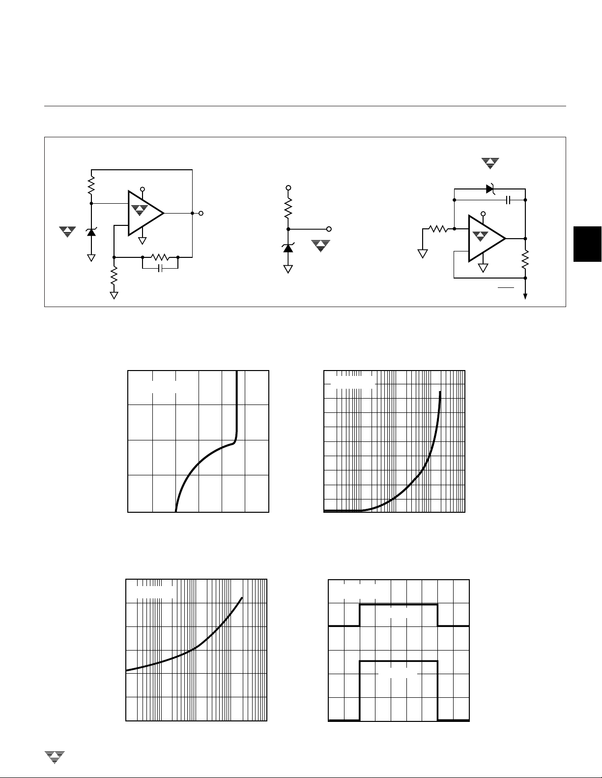
TYPICAL APPLICATIONS
1
TC9491A
TC9491B
10V Reference Battery Powered 1.25V Reference
3
2
30 kΩ
+15V
+
TC911
–
7
6
4
180 kΩ
0.1 µF
50 k Ω
1.22V
TC9491
TYPICAL CHARACTERISTICS
Output Voltage vs. Reverse Current
1000
= +25°C
T
A
100
10
2
2
3
TC9491
+15V
–
TC911
+
I
OUT
1µF
7
6
4
1.22V
=
R
SET
R
SET
3
+9V
V
= 10V
OUT
360 kΩ
81 kΩ
1.25V
TC9491
4
Output Voltage Change vs. Reverse Current
10
= +25°C
T
A
8
6
5
4
1
REVERSE CURRENT (µA)
0.1
0 0.25 0.5 0.75 1.0 1.25
OUTPUT VOLTAGE (V)
Forward Voltage vs. Forward Current
1.2
TA = +25°C
1.0
0.8
0.6
0.4
FORWARD VOLTAGE (V)
0.2
0
0.01 0.1 1 10 100
FORWARD CURRENT (mA)
TELCOM SEMICONDUCTOR, INC.
1.5
2
OUTPUT VOLTAGE CHANGE (mV)
0
0.01 0.1 1 10 100
REVERSE CURRENT (mA)
Response Time
10.0
= +25°C
T
A
5.0
1.5
VOLTAGE (V)
1.0
0.5
INPUT
0
OUTPUT
0
0 200 400 600
TIME (µsec)
6
7
8
3-17
 Loading...