


TC4420/TC4429
5-Pin TO-220
V
DD
GND
INPUT
GND
OUTPUT
TC4420
TC4429
Tab is
Common
to V
DD
8-Pin CERDIP/
1
2
3
4
V
DD
5
6
7
8
OUTPUT
GND
V
DD
INPUT
NC
GND
OUTPUT
TC4420
TC4429
TC4420 TC4429
V
DD
OUTPUT
GND
OUTPUT
PDIP/SOIC
Note 1: Duplicate pins must both be connected for proper operation.
2: Exposed pad of the DFN package is electrically isolated.
8-Pin DFN
(2)
V
DD
INPUT
NC
GND
2
3
4
5
6
7
8
1
TC4420
TC4429
V
DD
OUTPUT
GND
OUTPUT
TC4420 TC4429
V
DD
OUTPUT
GND
OUTPUT
6A High-Speed MOSFET Drivers
Features
• Latch-Up Protected: Will Withstand >1.5A
Reverse Output Current
• Logic Input Will Withstand Negative Swing Up To
5V
• ESD Protected: 4 kV
• Matched Rise and Fall Times:
- 25 ns (2500 pF load)
• High Peak Output Current: 6A
• Wide Input Supply Voltage Operating Range:
- 4.5V to 18V
• High Capacitive Load Drive Capability: 10,000pF
• Short Delay Time: 55 ns (typ.)
• CMOS/TTL Compatible Input
• Low Supply Current With Logic ‘1’ Input:
-450µA (typ.)
• Low Output Impedance: 2.5
• Output Voltage Swing to Within 25 mV of Ground
or V
DD
• Space-Saving 8-Pin SOIC and 8-Pin 6x5 DFN
Packages
Applications
General Description
The TC4420/TC4429 are 6A (peak), single-output
MOSFET drivers. The TC4429 is an inverting driver
(pin-compatible with the TC429), while the TC4420 is a
non-inverting driver. These drivers are fabricated in
CMOS for lower power and more efficient operation
versus bipolar drivers.
Both devices have TTL/CMOS compatible inpu ts that
can be driven as high a s V
without upset or damage to th e device. T his elimi nates
the need for external level-shifting circuitry and its
associated cost and size. The output swing is rail-to-rail,
ensuring better dri ve voltage margin, espe cially during
power-up/power-down sequencing. Propagational
delay time is only 55 ns (typ.) and the output rise and fall
times are only 25 ns (typ.) into 2500 pF across the
usable power supply range.
Unlike other drivers, the TC4420/TC4429 are virtually
latch-up proof. They replace three or more discrete
components, saving PCB area, parts and improving
overall system reliability.
+ 0.3V or as low as –5V
DD
• Switch-Mode Power Supp lie s
• Motor Controls
• Pulse Transformer Driver
• Class D Switching Amplifiers
(1)
Package Types
2002-2012 Microchip Technology Inc. DS21419D-page 1

TC4420/TC4429
Effective
Input
TC4420
Output
Input
GND
V
DD
300 mV
4.7V
C = 38 pF
TC4429
500 µA
Non-Inverting
Inverting
Functional Block Diagram
DS21419D-page 2 2002-2012 Microchip Technology Inc.

TC4420/TC4429
1.0 ELECTRICAL
CHARACTERISTICS
Absolute Maximum Ratings†
Supply Voltage.....................................................+20V
† Stresses above those listed under “Absolute Maximum
Ratings” may cause permanent damage to the device. These
are stress ratings only and functional operation of the device
at these or any other conditions above those indicated in the
operation sections of the specifications is not implied.
Exposure to Absolute Maximum Rating conditions for
extended periods may affect device reliability.
Input Voltage..................................– 5V to VDD + 0.3V
Input Current (VIN > VDD)...................................50 mA
Power Dissipation (T
70°C)
A
5-Pin TO-220....................................................1.6W
CERDIP.......................................................800 mW
DFN............................................ ...................Note 2
PDIP............................................................730 mW
SOIC............................................................470 mW
Package Power Dissipation (T
25°C)
A
5-Pin TO-220 (With Heatsink) ........................12.5W
Thermal Impedances (To Case)
5-Pin TO-220 R
......................................10°C/W
J-C
DC CHARACTERISTICS
Electrical Specifications: Unless otherwise noted, TA = +25°C with 4.5V VDD 18V.
Parameters Sym Min Typ Max Units Conditions
Input
Logic ‘1’, High Input
Voltage
Logic ‘0’, Low Input Voltage V
Input Voltage Range V
Input Current I
Output
High Output Voltage V
Low Output Voltage V
Output Resistanc e, Hi gh R
Output Resistanc e, Low R
Peak Output Current I
Latch-Up Protection
Withstand Reverse Current
Switching Time (Note 1)
Rise Time t
Fall Time t
Delay Time t
Delay Time t
Power Supply
Power Supply Current I
Operating Input Voltage V
Note 1: Switching times ensured by design.
2: Package power dissipation is dependent on the copper pad area on the PCB.
V
I
REV
IH
IL
IN
IN
OH
OL
OH
OL
PK
2.4 1.8 — V
—1.30.8V
–5 — VDD+0.3 V
–10 — +10 µA 0VVINV
VDD – 0.025 — — V DC TEST
— — 0.025 V DC TEST
—2.12.8 I
—1.52.5 I
—6.0—AV
— > 1.5 — A Duty cycle2%, t 300 µsec
R
F
D1
D2
S
DD
—2535nsFigure 4-1, CL = 2,500 pF
—2535nsFigure 4-1, CL = 2,500 pF
—5575nsFigure 4-1
—5575nsFigure 4-1
—
—
0.45
55
1.5
150
mAµAVIN = 3V
4.5 — 18 V
OUT
OUT
V
DD
IN
= 0V
DD
= 10 mA, VDD = 18V
= 10 mA, VDD = 18V
= 18V
2002-2012 Microchip Technology Inc. DS21419D-page 3

TC4420/TC4429
DC CHARACTERISTICS (OVER OPERATING TEMPERATURE RANGE)
Electrical Specifications: Unless otherwise noted, over operating temperature range with 4.5V VDD 18V.
Parameters Sym Min Typ Max Units Conditions
Input
Logic ‘1’, High Input
Voltage
Logic ‘0’, Low Input Voltage V
Input Voltage Range V
Input Current I
Output
High Output Voltage V
Low Output Voltage V
Output Resistanc e, Hi gh R
Output Resistanc e, Low R
Switching Time (Note 1)
Rise Time t
Fall Time t
Delay Time t
Delay Time t
Power Supply
Power Supply Current I
Operating Input Voltage V
Note 1: Switching times ensured by design.
V
IH
IL
IN
IN
OH
OL
OH
OL
R
F
D1
D2
S
DD
2.4 — — V
——0.8V
–5 — VDD + 0.3 V
–10 — +10 µA 0VVINV
VDD – 0.025 — — V DC TEST
— — 0.025 V DC TEST
—35 I
—2.35 I
—3260nsFigure 4-1, CL = 2,500 pF
—3460nsFigure 4-1, CL = 2,500 pF
—50100nsFigure 4-1
—65100nsFigure 4-1
—
—
0.45
60
3
400
4.5 — 18 V
= 10 mA, VDD = 18V
OUT
= 10 mA, VDD = 18V
OUT
mAµAVIN = 3V
V
= 0V
IN
DD
TEMPERATURE CHARACTERISTICS
Electrical Specifications: Unless otherwise noted, all parameters apply with 4.5V V
Parameters Sym Min Typ Max Units Conditions
Temperature Ranges
Specified Temperature Range (C) T
Specified Temperature Range (I) T
Specified Temperature Range (E) T
Specified Temperature Range (V) T
Maximum Junction Temperature T
Storage Temperature Range T
Package Thermal Resistances
Thermal Resistance, 5L-TO-220
Thermal Resistance, 8L-CERDIP
Thermal Resistance, 8L-6x5 DFN
Thermal Resistance, 8L-PDIP
Thermal Resistance, 8L-SOIC
A
A
A
A
J
A
JA
JA
JA
JA
JA
0—+70°C
–25 — +85 °C
–40 — +85 °C
–40 — +125 °C
— — +150 °C
–65 — +150 °C
—71—°C/W
—150—°C/W
— 33.2 — °C/W Typical four-layer board
—125—°C/W
—155—°C/W
18V.
DD
with vias to ground plane.
DS21419D-page 4 2002-2012 Microchip Technology Inc.

TC4420/TC4429
V = 12V
DD
V = 5V
DD
60
40
20
10
1000
10,000
Capcitive Load (pF)
V = 18V
DD
80
100
Time (nsec)
50
40
30
20
10
0
–60 –20 20 60 100
140
TA (°C)
Delay Time (nsec)
D1
t
D2
t
C = 2200 pF
L
V = 18V
DD
0
2.0 TYPICAL PERFORMANCE CURVES
Note: The graphs and ta bles provided followi ng thi s n ote are a statistical s umm ar y based on a limited number of
samples and are provided for informational purposes only. The performance characteristics listed herein
are not tested or guaranteed. In some graphs or tables, the data presented may be outside the specified
operating range (e.g., outside specified power supply range) and therefore outside the warranted range.
Note: Unless otherwise indicated, TA = +25°C with 4.5V VDD 18V.
120
100
C = 10,000 pF
80
60
Time (nsec)
40
20
0
579111315
Supply Voltage (V)
L
C = 4700 pF
L
C = 2200 pF
L
FIGURE 2-1: Rise Time vs. Supply Voltage.
100
80
C = 10,000 pF
60
40
Time (nsec)
20
0
57 9111315
Supply Voltage (V)
L
C = 4700 pF
L
C = 2200 pF
L
FIGURE 2-4: Fall Time vs. Supply Voltage.
100
80
60
40
V = 5V
DD
V = 12V
Time (nsec)
20
10
1000
DD
Capacitive Load (pF)
V = 18V
DD
10,00
FIGURE 2-2: Rise Time vs. Capacitive Load.
FIGURE 2-3: Propagation Delay Time vs. Temperature.
2002-2012 Microchip Technology Inc. DS21419D-page 5
FIGURE 2-5: Fall Time vs. Capacitive Load.
84
V = 15V
DD
70
56
42
28
Supply Current (mA)
14
0
0 100 1000
500 kHz
200 kHz
Capacitive Load (pF)
20 kHz
10,000
FIGURE 2-6: Supply Current vs. Capacitive Load.

TC4420/TC4429
–60 –20 20 60 100
140
TA (°C)
t
RISE
t
50
40
30
20
10
0
Time (nsec)
C = 2200 pF
V = 18V
DD
FALL
L
65
60
55
50
45
40
35
Delay Time (nsec)
4 6 81012141618
Supply Voltage (V)
t
D2
t
D1
100
0
0 100 1000
10,000
Frequency (kHz)
Supply Current (mA)
10
1000
18V
10V
5V
C = 2200 pF
L
5
200
160
120
80
40
0
Delay Time (nsec)
567 11 13
15
Load = 2200 pF
Input 2.4V
Input 3V
Input 5V
Input 8V and 10V
8 9 10 12 14
V (V)
DD
Note: Unless otherwise indicated, TA = +25°C with 4.5V VDD 18V.
5
FIGURE 2-7: Rise and Fall Times vs. Temperature.
100 mA
10 mA
5913
7111
Supply Voltage (V)
50 mA
OUT
R ( )Ω
4
3
2
FIGURE 2-10: High-State Output Resistance vs Supply Voltage.
FIGURE 2-8: Propagation Delay Time vs. Supply Voltage.
FIGURE 2-9: Supply Current vs. Frequency.
DS21419D-page 6 2002-2012 Microchip Technology Inc.
FIGURE 2-11: Effect of Input Amplitude on Propagation Delay.
2.5
2
OUT
R ( )Ω
1.5
1
5913
71115
Supply Voltage (V)
100 mA
50 mA
10 mA
FIGURE 2-12: Low-State Output Resistance vs. Supply Voltage.

Note: Unless otherwise indicated, TA = +25°C with 4.5V VDD 18V.
4
3
2
1
0
Crossover Area (A•S) x 10
-8
567 11 13
15
8 9 10 12 14
Supply Voltage (V)
The values on this graph represent the loss seen
by the driver during one complete cycle. For a
single transition, divide the value by 2.
FIGURE 2-13: Crossover Energy.
TC4420/TC4429
2002-2012 Microchip Technology Inc. DS21419D-page 7

TC4420/TC4429
3.0 PIN DESCRIPTIONS
The descriptions of the pins are listed in Table 3-1.
TABLE 3-1: PIN FUNCTION TABLE
Pin No.
8-Pin CERDIP/
PDIP/SOIC
11—VDDSupply input, 4.5V to 18V
2 2 1 INPUT Control input, TTL/CMOS compatible input
3 3 — NC No Connection
4 4 2 GND Ground
5 5 4 GND Ground
6 6 5 OUTPUT CMOS push-pull output
7 7 — OUTPUT CMOS push-pull output
883V
—PAD— NCExposed Metal Pad
——TABV
3.1 Supply Input (VDD)
The VDD input is the bias supp ly for the MO SFET driver
and is rated for 4.5V to 18V with respect to the ground
pins. The VDD input should be bypassed to ground with
a local ceramic capacitor. The value of the capacito r
should be chos en base d on the c apacitiv e load th at is
being driven. A minimum val ue of 1. 0µF is suggested.
Pin No.
8-Pin DFN
Pin No.
5-Pin TO-220
Symbol Description
DD
DD
Supply input, 4.5V to 18V
Metal Tab is at the VDD Potential
3.3 CMOS Push-Pull Output
The MOSFET driver output is a low-impedance,
CMOS, push-pull style output capable of driving a
capacitive load with 6.0A peak currents. The MOSFET
driver output is capable of withstanding 1.5A peak
reverse currents of either polarity.
3.4 Ground
3.2 Control Input
The MOSFET driver input is a high-impedance,
TTL/CMOS compatible input. The input circuitry of the
TC4420/TC4429 MOSFET driver also has a “speedup” capacitor. This helps to decrease the propagation
delay times of the driver. Because of this, input signals
with slow rising or falling edges should not be us ed, a s
this can result in double-pulsing of the MOSFET driver
output.
The ground pins are the return path for the bias current
and the high peak currents that discharge the load
capacitor . The ground pins sh ould be tied into a ground
plane or have very short traces to the bias supply
source return.
3.5 Exposed Metal Pad
The exposed met al p ad of the 6x5 DFN pac ka ge i s n ot
internally connected to any potential. Therefore, this
pad can be connected to a ground plane or other
copper plane on a printed circuit board (PCB) to aid in
heat removal from the package.
DS21419D-page 8 2002-2012 Microchip Technology Inc.

4.0 APPLICATIONS INFORMATION
Inverting Driver
Non-Inverting Driver
Input
t
D1
t
F
t
R
t
D2
Input: 100 kHz,
square wave,
t
RISE
= t
FALL
10 ns
Output
Input
Output
t
D1
t
F
t
R
t
D2
+5V
10%
90%
10%
90%
10%
90%
+18V
0V
90%
10%
10%
10%
90%
+5V
+18V
0V
0V
0V
90%
26
7
54
18
CL = 2,500 pF
0.1 µF
4.7 µF
Input
V
DD
= 18V
Output
0.1 µF
Note: Pinout shown is for the PDIP, SOIC, DFN and CERDIP packages.
TC4429
TC4420
TC4420/TC4429
FIGURE 4-1: Switching Time Test Circuits.
2002-2012 Microchip Technology Inc. DS21419D-page 9

TC4420/TC4429
5-Lead TO-220
XXXXXXXXX
XXXXXXXXX
YYWWNNN
Example:
TC4420CAT
0419256
8-Lead CERDIP (300 mil)
Example:
XXXXXXXX
XXXXXNNN
YYWW
TC4420
MJA256
0419
8-Lead DFN
Example
:
XXXXXXX
XXXXXXX
XXYYWW
NNN
TC4420
EMF
0419
256
Legend: XX...X Customer-specific information
Y Year code (last digit of calendar year)
YY Year code (last 2 digits of calendar year)
WW Week code (week of January 1 is week ‘01’)
NNN Alphanumeric traceability code
Pb-free JEDEC designator for Matte Tin (Sn)
* This package is Pb-free. The Pb-free JEDEC designator ( )
can be found on the outer packaging for this package.
Note: In the event the full Microchip part num ber can not be ma rke d on one li ne, it will
be carried over to the next line, thus limiting the number of available
characters for customer-specific information.
3
e
5.0 PACKAGING INFORMATION
5.1 Package Marking Information
DS21419D-page 10 2002-2012 Microchip Technology Inc.
3
e

Package Marking Information (Continued)
XXXXXXXX
XXXXXNNN
YYWW
8-Lead PDIP (300 mil)
Example:
TC4420
CPA256
0419
8-Lead SOIC (150 mil)
Example:
XXXXXXXX
XXXXYYWW
NNN
TC4420
EOA0419
256
TC4420/TC4429
2002-2012 Microchip Technology Inc. DS21419D-page 11

TC4420/TC4429
L H1
Q
E
b
e1
e
C1
J1
F
A
D
a
(5X)
ØP
EJECTOR PIN
e3
Drawing No. C04-036
Notes:
Dimensions D and E1 do not include mold flash or protrusions. Mold flash or
protrusions shall not exceed .010" (0.254mm) per side.
JEDEC equivalent: TO-220
*Controlling Parameter
Mold Draft Angle
Lead Width
Lead Thickness
a
C1
b
.014
Dimension Limits
Overall Height
Lead Length
Overall Width
Lead Pitch
A
L
E
.540
MIN
e
Units
.060
INCHES*
.022 0.36 0.56
MILLIMETERS
.190
.560 13.72
MINMAX
4.83
14.22
MAX
.160 4.06
3° 7° 3° 7°
Overall Length D
1.020.64.040.025
Overall Lead Centers e1 .263
.385
.560
.273 6.68 6.93
.072 1.52 1.83
.415 9.78 10.54
.590 14.22 14.99
Through Hole Diameter P .146 .156 3.71 3.96
J1Base to Bottom of Lead .090 2.29.115 2.92
Through Hole Center
Q
.103 2.87.113 2.62
Flag Thickness F .045 1.40.055 1.14
Flag Length H1 .234 6.55.258 5.94
Space Between Leads e3 .030 1.02.040 0.76
Note: For the most current package drawings, please see the Microchip Packaging Specification located
at http://www.microchip.com/packaging
5-Lead Plastic Transistor Outline (AT) (TO-220)
DS21419D-page 12 2002-2012 Microchip Technology Inc.

8-Lead Ceramic Dual In-line – 300 mil (JA) (CERDIP)
10.169.158.13.400.360.320
eB
Overall Row Spacing
0.510.460.41.020.018.016BLower Lead Width
1.651.401.14.065.055.045
B1
Upper Lead Width
0.380.290.20.015.012.008
c
Lead Thickness
5.084.133.18.200.163.125LTip to Seating Plane
10.169.789.40.400.385.370DOverall Length
7.626.735.84.300.265.230
E1
Ceramic Pkg. Width
8.137.757.37.320.305.290EShoulder to Shoulder Width
1.020.770.51.040.030.020
A1
Standoff §
5.084.574.06.200.180.160ATop to Seating Plane
2.54.100
p
Pitch
88
n
Number of Pins
MAX
NOM
MINMAX
NOM
MINDimension Limits
MILLIMETERSINCHES*Units
JEDEC Equivalent: MS-030
Drawing No. C04-010
*Controlling Parameter
Note: For the most current package drawings, please see the Microchip Packaging Specification located
at http://www.microchip.com/packaging
E1
TC4420/TC4429
n
2
1
D
E
A2
A
eB
c
B1
A1
B
p
L
2002-2012 Microchip Technology Inc. DS21419D-page 13

TC4420/TC4429
Note: For the most current package drawings, please see the Microchip Packaging Specification located
at http://www.m ic roc hip.c om /p a ckagi ng
8-Lead Plastic Dual Flat No Lead Package (MF) 6x5 mm Body (DFN-S) – Saw Singulated
DS21419D-page 14 2002-2012 Microchip Technology Inc.

TC4420/TC4429
B1
B
A1
A
L
A2
p
E
eB
c
E1
n
D
1
2
Units INCHES* MILLIMETERS
Dimension Limits MIN NOM MAX MIN NOM MAX
Number of Pins
n
88
Pitch
p
.100 2.54
Top to Seating Plane A .140 .155 .170 3.56 3.94 4.32
Molded Package Thickness A2 .115 .130 .145 2.92 3.30 3.68
Base to Seating Plane A1 .015 0.38
Shoulder to Shoulder Width E .300 .313 .325 7.62 7.94 8.26
Molded Package Width E1 .240 .250 .260 6.10 6.35 6.60
Overall Length D .360 .373 .385 9.14 9.46 9.78
Tip to Seating Plane L .125 .130 .135 3.18 3.30 3.43
Lead Thickness
c
.008 .012 .015 0.20 0.29 0.38
Upper Lead Width B1 .045 .058 .070 1.14 1.46 1.78
Lower Lead Width B .014 .018 .022 0.36 0.46 0.56
Overall Row Spacing § eB .310 .370 .430 7.87 9.40 10.92
Mold Draft Angle Top
51015 51015
Mold Draft Angle Bottom
51015 51015
* Controlling Parameter
Notes:
Dimensions D and E1 do not include mold flash or protrusions. Mold flash or protrusions shall not exceed
JEDEC Equivalent: MS-001
Drawing No. C04-018
.010” (0.254mm) per side.
§ Significant Characteristic
Note: For the most current package drawings, please see the Microchip Packaging Specification located
at http://www .m ic roc hip .c om/ p ac k agi ng
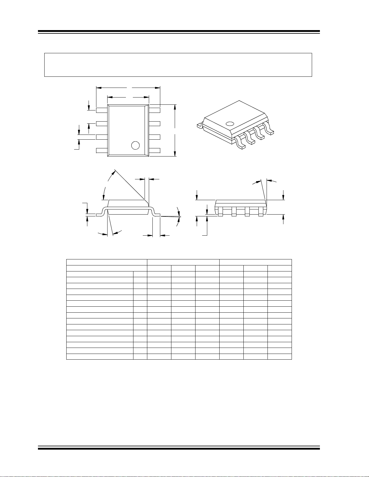
8-Lead Plastic Dual In-line (PA) – 300 mil (PDIP)
2002-2012 Microchip Technology Inc. DS21419D-page 15
TC4420/TC4429
Foot Angle
048048
1512015120
Mold Draft Angle Bottom
1512015120
Mold Draft Angle Top
0.510.420.33.020.017.013BLead Width
0.250.230.20.010.009.008
c
Lead Thickness
0.760.620.48.030.025.019LFoot Length
0.510.380.25.020.015.010hChamfer Distance
5.004.904.80.197.193.189DOverall Length
3.993.913.71.157.154.146E1Molded Package Width
6.206.025.79.244.237.228EOverall Width
0.250.180.10.010.007.004A1Standoff §
1.551.421.32.061.056.052
A2
Molded Package Thickness
1.751.551.35.069.061.053AOverall Height
1.27.050
p
Pitch
88
n
Number of Pi ns
MAXNOMMINMAXNOMMINDimension Limits
MILLIMETERSINCHES*Units
2
1
D
n
p
B
E
E1
h
L
c
45
A2
A
A1
* Controlling Parameter
Notes:
Dimensions D and E1 do not include mold flash or protrusions. Mold flash or protrusions shall not exceed
.010” (0.254mm) per side.
JEDEC Equivalent: MS-012
Drawing No. C04-057
§ Significant Characteristic
Note: For the most current package drawings, please see the Microchip Packaging Specification located
at http://www.microchip.com/packaging
8-Lead Plastic Small Outline (OA) – Narrow, 150 mil (SOIC)
DS21419D-page 16 2002-2012 Microchip Technology Inc.

6.0 REVISION HISTORY
Revision D (December 2012)
Added a note to each package outline drawing.
TC4420/TC4429
2002-2012 Microchip Technology Inc. DS21419D-page 17

TC4420/TC4429
NOTES:
DS21419D-page 18 2002-2012 Microchip Technology Inc.

TC4420/TC4429
Device: TC4420: 6A High-Speed MOSFET Driver, Non-Inverting
TC4429: 6A High-Speed MOSFET Driver, Inverting
Temperature Range: C = 0°C to +70°C (PDIP, SOIC, and TO-220 Only)
I = -25°C to +85°C (CERDIP Only)
E = -40°C to +85°C
V = -40°C to +125°C
Package: AT = TO-220, 5-lead (C-Temp Only)
JA = Ceramic Dual In-line (300 mil Body), 8-lead
(I-Temp Only)
MF = Dual, Flat, No-Lead (6X5 mm Body), 8-lead
MF713 = Dual, Flat, No-Lead (6X5 mm Body), 8-lead
(Tape and Reel)
PA = Plastic DIP (300 mil Body), 8-lead
OA = Plastic SOIC, (150 mil Body), 8-lead
OA713 = Plastic SOIC, (150 mil Body), 8-lead
(Tape and Reel)
PB Free G = Lead-Free device*
= Blank
* Available on selected packages. Contact your local sales
representative for availability
PART NO. X XX
PackageTemperature
Range
Device
Examples:
a) TC4420CAT: 6A High-Speed MOSFET
Driver, Non-inverting,
TO-220 package,
0°C to +70°C.
b) TC4420EOA:
6A High-Speed MOSFET
Driver, Non-inverting,
SOIC package,
-40°C to +85°C.
c) TC4420VMF:
6A High-Speed MOSFET
Driver, Non-inverting,
DFN package,
-40°C to +125°C.
a) TC4429CAT:
6A High-Speed MOSFET
Driver, Inverting,
TO-220 package,
0°C to +70°C
b) TC4429EPA:
6A High-Speed MOSFET
Driver, Inverting,
PDIP package,
-40°C to +85°C
c) TC4429VMF:
6A High-Speed MOSFET
Driver, Inverting,
DFN package,
-40°C to +125°C
XXX
Tape and
Reel
X
PB Free
PRODUCT IDENTIFICATION SYSTEM
To order or obtain information, e.g., on pricing or delivery, refer to the factory or the listed sales office.
Sales and Support
Data Sheets
Products supported by a preliminary Data Sheet may have an errata sheet describing minor operational differences and
recommended workarounds. To determine if an errata sheet exists for a particular device, please contact one of the following:
1. Your local Microchip sales office
2. The Microchip Worldwide Site (www.microchip.com)
Please specify which device, revision of silicon and Data Sheet (include Literature #) you are using.
Customer Notification System
Register on our web site (www.microchip.com/cn) to receive the most current information on our products.
2002-2012 Microchip Technology Inc. DS21419D-page 19

TC4420/TC4429
NOTES:
DS21419D-page 20 2002-2012 Microchip Technology Inc.

Note the following details of the code protection feature on Microchip devices:
YSTEM
CERTIFIED BY DNV
== ISO/TS 16949 ==
• Microchip products meet the specification contained in their particular Microchip Data Sheet.
• Microchip believes that its family of products is one of the most secure families of its kind on the market t oday, when used in the
intended manner and under normal conditions.
• There are dishonest and possibly illegal methods used to breach the code protection feature. All of these methods, to our
knowledge, require using the Microchip products in a manner outside the operating specifications contained in Microchip’s Data
Sheets. Most likely, the person doing so is engaged in theft of intellectual property.
• Microchip is willing to work with the customer who is concerned about the integrity of their code.
• Neither Microchip nor any other semiconductor manufacturer can guarantee the security of their code. Code protection does not
mean that we are guaranteeing the product as “unbreakable.”
Code protection is constantly evolving. We at Microchip are com mitted to continuously improving the c ode prot ection f eatures of our
products. Attempts to break Microchip’s code protection feature may be a violation of t he Digit al Mill ennium Copyright Act. If such act s
allow unauthorized access to your software or other copyrighted work, you may have a right to sue for relief under that Act.
Information contained in this publication regarding device
applications and t he lik e is provided only for your convenience
and may be su perseded by upda t es . It is y our responsibility to
ensure that your application meets with your specifications.
MICROCHIP MAKES NO REPRESENTATIONS OR
WARRANTIES OF ANY KIND WHETHER EXPRESS OR
IMPLIED, WRITTEN OR ORAL, STATUTORY OR
OTHERWISE, RELATED TO THE INFORMATION,
INCLUDING BUT NOT LIMITED TO ITS CONDITION,
QUALITY, PERFORMANCE, MERCHANTABILITY OR
FITNESS FOR PURPOSE. Microchip disclaims all liability
arising from this information and its use. Use of Microchip
devices in life supp ort and/or safety ap plications is entir ely at
the buyer’s risk, and the buyer agrees to defend, indemnify and
hold harmless M icrochip from any and all dama ges, claims,
suits, or expenses re sulting from such use. No licens es are
conveyed, implicitly or otherwise, under any Microchip
intellectual property rights.
Trademarks
The Microchip name and logo, the Microchip logo, dsPIC,
FlashFlex, K
PICSTART, PI C
and UNI/O are registered trademarks of Microchip T echnology
Incorporated in the U.S.A. and other countries.
FilterLab, Hampshire, HI-TECH C, Linear Active Thermistor,
MTP, SEEVAL and The Embedded Control Solutions
Company are registered trademarks of Microchip Technology
Incorporated in the U.S.A.
Silicon Storage Technology is a registered trademark of
Microchip Technology Inc. in other countries.
Analog-for-the-Digital Age, Application Maestro, BodyCom,
chipKIT, chipKIT logo, CodeGuard, dsPICDEM,
dsPICDEM.net, dsPICworks, dsSPEAK, ECAN,
ECONOMONITOR, FanSense, HI-TIDE, In-Circuit Serial
Programming, ICSP, Mindi, MiWi, MPASM, MPF, MPLAB
Certified logo, MPLIB, MPLINK, mTouch, Omniscient Code
Generation, PICC, PICC-18, PICDEM, PICDEM.net, PICkit,
PICtail, REAL ICE, rfLAB, Select Mode, SQI, Serial Quad I/O,
Total Endurance, TSHARC, UniWinDriver, WiperLock, ZENA
and Z-Scale are trademarks of Microchip Technology
Incorporated in the U.S.A. and other countries.
SQTP is a service mark of Microchip T echnology Incorporated
in the U.S.A.
GestIC and ULPP are registered trademarks of Microchip
Technology Germany II GmbH & Co. & KG, a subsidiary of
Microchip T echnology Inc., in other countries.
All other trademarks mentioned herein are property of their
respective companies.
© 2002-2012, Microchip Technology Incorporated, Printed in
the U.S.A., All Rights Reserved.
Printed on recycled paper.
ISBN: 9781620767948
EELOQ, KEELOQ logo, MPLAB, PIC, PICmicro,
32
logo, rfPIC, SST, SST Logo, SuperFlash
QUALITY MANAGEMENT S
2002-2012 Microchip Technology Inc. DS21419D-page 21
Microchip received ISO/TS-16949:2009 certification for its worldwide
headquarters, design and wafer fabrication facilities in Chandler and
Tempe, Arizona; Gresham, Oregon and design centers in California
and India. The Company’s quality system processes and procedures
are for its PIC
devices, Serial EEPROMs, microperipherals, nonvolatile memory and
analog products. In addition, Microchip’s quality system for the design
and manufacture of development systems is ISO 9001:2000 certified.
®
MCUs and dsPIC® DSCs, KEELOQ
®
code hopping

Worldwide Sales and Service
AMERICAS
Corporate Office
2355 West Chandler Blvd.
Chandler, AZ 85224-6199
Tel: 480-792-7200
Fax: 480-792-7277
Technical Support:
http://www.microchip.com/
support
Web Address:
www.microchip.com
Atlanta
Duluth, GA
Tel: 678-957-9614
Fax: 678-957-1455
Boston
Westborough, MA
Tel: 774-760-0087
Fax: 774-760-0088
Chicago
Itasca, IL
Tel: 630-285-0071
Fax: 630-285-0075
Cleveland
Independence, OH
Tel: 216-447-0464
Fax: 216-447-0643
Dallas
Addison, TX
Tel: 972-818-7423
Fax: 972-818-2924
Detroit
Farmington Hills, MI
Tel: 248-538-2250
Fax: 248-538-2260
Indianapolis
Noblesville, IN
Tel: 317-773-8323
Fax: 317-773-5453
Los Angeles
Mission Viejo, CA
Tel: 949-462-9523
Fax: 949-462-9608
Santa Clara
Santa Clara, CA
Tel: 408-961-6444
Fax: 408-961-6445
Toronto
Mississauga, Ontario,
Canada
Tel: 905-673-0699
Fax: 905-673-6509
ASIA/PACIFIC
Asia Pacific Office
Suites 3707-14, 37th Floor
Tower 6, The Gateway
Harbour City, Kowloon
Hong Kong
Tel: 852-2401-1200
Fax: 852-2401-3431
Australia - Sydney
Tel: 61-2-9868-6733
Fax: 61-2-9868-6755
China - Beijing
Tel: 86-10-8569-7000
Fax: 86-10-8528-2104
China - Chengdu
Tel: 86-28-8665-5511
Fax: 86-28-8665-7889
China - Chongqing
Tel: 86-23-8980-9588
Fax: 86-23-8980-9500
China - Hangzhou
Tel: 86-571-2819-3187
Fax: 86-571-2819-3189
China - Hong Kong SAR
Tel: 852-2943-5100
Fax: 852-2401-3431
China - Nanjing
Tel: 86-25-8473-2460
Fax: 86-25-8473-2470
China - Qingdao
Tel: 86-532-8502-7355
Fax: 86-532-8502-7205
China - Shanghai
Tel: 86-21-5407-5533
Fax: 86-21-5407-5066
China - Shenyang
Tel: 86-24-2334-2829
Fax: 86-24-2334-2393
China - Shenzhen
Tel: 86-755-8864-2200
Fax: 86-755-8203-1760
China - Wuhan
Tel: 86-27-5980-5300
Fax: 86-27-5980-5118
China - Xian
Tel: 86-29-8833-7252
Fax: 86-29-8833-7256
China - Xiamen
Tel: 86-592-2388138
Fax: 86-592-2388130
China - Zhuhai
Tel: 86-756-3210040
Fax: 86-756-3210049
ASIA/PACIFIC
India - Bangalore
Tel: 91-80-3090-4444
Fax: 91-80-3090-4123
India - New Delhi
Tel: 91-1 1-4160-8631
Fax: 91-11-4160-8632
India - Pune
Tel: 91-20-2566-1512
Fax: 91-20-2566-1513
Japan - Osaka
Tel: 81-66-152-7160
Fax: 81-66-152-9310
Japan - Yokohama
Tel: 81-45-471- 6166
Fax: 81-45-471-6122
Korea - Daegu
Tel: 82-53-744-4301
Fax: 82-53-744-4302
Korea - Seoul
Tel: 82-2-554-7200
Fax: 82-2-558-5932 or
82-2-558-5934
Malaysia - Kuala Lumpur
Tel: 60-3-6201-9857
Fax: 60-3-6201-9859
Malaysia - Penang
Tel: 60-4-227-8870
Fax: 60-4-227-4068
Philippines - Manila
Tel: 63-2-634-9065
Fax: 63-2-634-9069
Singapore
Tel: 65-6334-8870
Fax: 65-6334-8850
Tai wan - Hsin Chu
Tel: 886-3-5778-366
Fax: 886-3-5770-955
Taiwan - Kaohsiung
Tel: 886-7-213-7828
Fax: 886-7-330-9305
Taiwan - Taipei
Tel: 886-2-2508-8600
Fax: 886-2-2508-0102
Thailand - Bangkok
Tel: 66-2-694-1351
Fax: 66-2-694-1350
EUROPE
Austria - Wels
Tel: 43-7242-2244-39
Fax: 43-7242-2244-393
Denmark - Copenhagen
Tel: 45-4450-2828
Fax: 45-4485-2829
France - Paris
Tel: 33-1-69-53-63-20
Fax: 33-1-69-30-90-79
Germany - Munich
Tel: 49-89-627-144-0
Fax: 49-89-627-144-44
Italy - Milan
Tel: 39-0331-742611
Fax: 39-0331-466781
Netherlands - Drunen
Tel: 31-416-690399
Fax: 31-416-690340
Spain - Madrid
Tel: 34-91-708-08-90
Fax: 34-91-708-08-91
UK - Wokingham
Tel: 44-118-921-5869
Fax: 44-118-921-5820
11/27/12
DS21419D-page 22 2002-2012 Microchip Technology Inc.
 Loading...