

Page 1
TAFE1040
3 V, 10-BIT 42 MSPS, AREA CCD ANALOG FRONT-END
SLVS284 – FEBRUAR Y 2000
features
D
Single-Chip CCD Analog Front-End
D
10-Bit, 42 MSPS, A/D Converter
D
Single 3-V Supply Operation
D
Programmable Timing Signal Delays
D
Low Power: 180 mW Typ, 2-mW
applications
D
Video Camcorde
D
Digital Still Camera
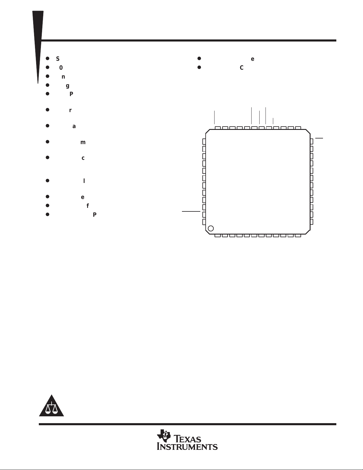
PFB PACKAGE
(TOP VIEW)
Power-down Mode
D
Differential Nonlinearity Error
– <±0.6 LSB Typ
D
Integral Nonlinearity Error
– <±1.5 LSB Typ
D
Programmable Gain Amplifier (PGA) With
0 dB to 36 dB Gain Range (0.045 dB/Step)
D
Automatic or Programmable Black Level
and Offset Calibration With Digital Filter
and Bad Pixel Limits
D
Additional DACs for External Analog
Setting
D
Serial Interface for Register Configuration
D
Internal Reference Voltages
D
48-Pin TQFP Package
description
The TAFE1040 is a complete area CCD analog
front-end/digitizer designed for digital camera
applications. The TAFE1040 performs all the
AGND5
RBD
RMD
RPD
AVDD5
VSS
AVDD1
AGND1
SR
SV
CLAMP
CLREF
BLKG
TPP
35 34 33 32 3136 30
37
38
39
40
41
42
43
44
45
46
47
48
23
1
PIN
DIN
TPM
AVDD4
5678
4
AVDD2
AGND2
AGND4
OBCLP
DVDD
DGND
RESETCSSDIN
STBY
28 27 2629
D0D1D2
10 11 12
9
SCLK
ADCCLK
25
D3D4D5
24
23
22
21
20
19
18
17
16
15
14
13
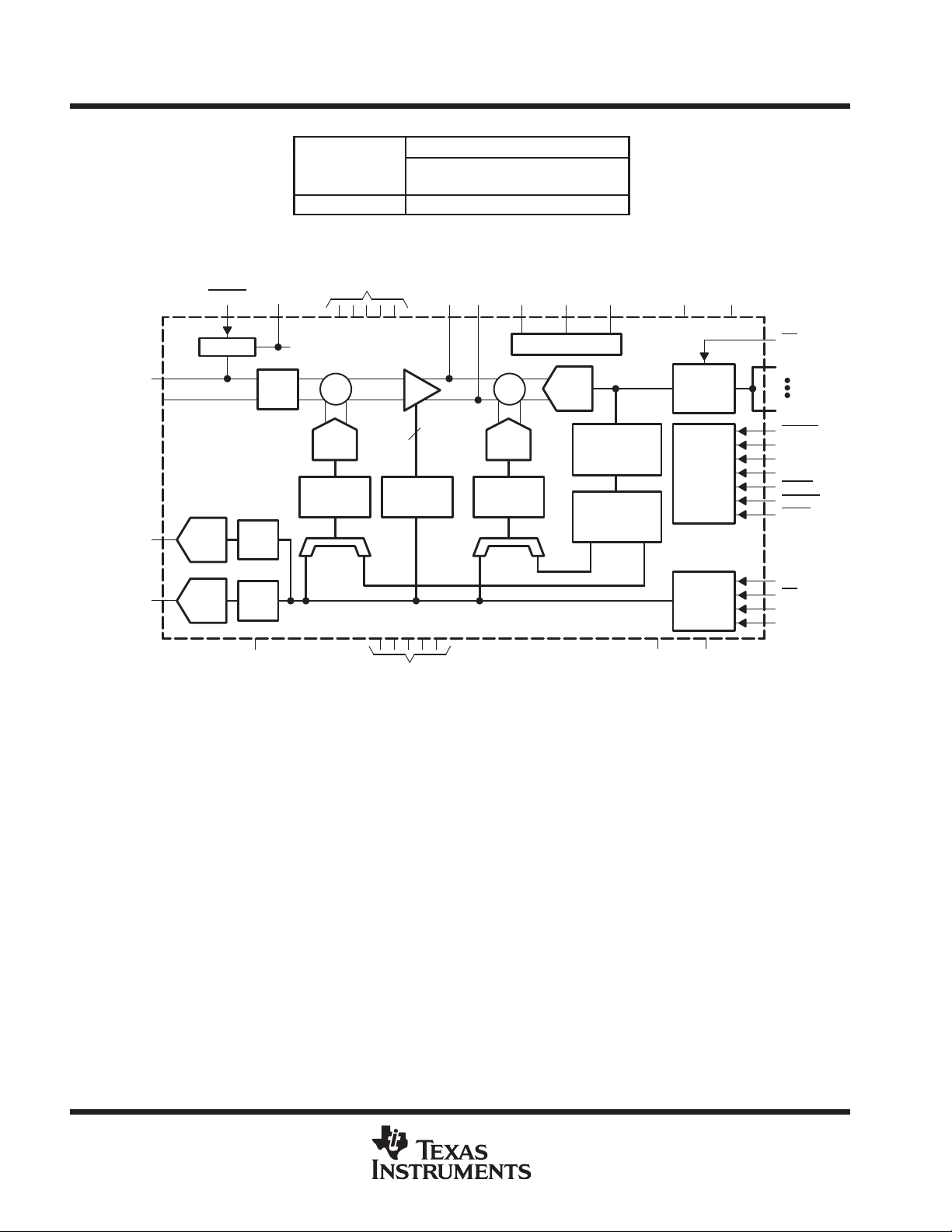
analog processing functions necessary to maxmize the dynamic range, corrects various errors associated with the CCD sensor, and then digitizes the results
with an on-chip high-speed analog-to-digital converter (ADC). The key components of the T AFE1040 include:
input clamp circuitry for the CCD and analog video signals, a correlated double sampler (CDS), a programmable
gain amplifier (PGA) with 0 dB to 36 dB gain range, two internal digital-to-analog converters (DAC) for automatic
or programmable optical black level and offset calibration, a 10-bit, 42 MSPS pipeline ADC, a parallel data port
for easy microprocessor interface and a serial port for configuring internal control registers, two additional DACs
for external system control, and internal reference voltages.
OE
SCKP
DACO2
DACO1
AGND3
A VDD3
DIGND
DIVDD
D9
D8
D7
D6
PRODUCT PREVIEW
Designed in advanced CMOS process, the T AFE1040 operates from a single 3-V power supply with a normal
power consumption of 180 mW at 42 MSPS and a 2-mW power-down mode.
Very high throughput rate, single 3 V operation, low power consumption, and fully integrated analog processing
circuitry make the T AFE1040 an ideal area CCD signal processing solution for the high-resolution digital camera
and camcorder applications.
The part is available in a 48-pin TQFP package and is specified over –20°C to 75°C operating temperature
range.
Please be aware that an important notice concerning availability, standard warranty, and use in critical applications of
Texas Instruments semiconductor products and disclaimers thereto appears at the end of this data sheet.
PRODUCT PREVIEW information concerns products in the formative or
design phase of development. Characteristic data and other
specifications are design goals. Texas Instruments reserves the right to
change or discontinue these products without notice.
POST OFFICE BOX 655303 • DALLAS, TEXAS 75265
Copyright 2000, Texas Instruments Incorporated
1
Page 2
TAFE1040
3 V, 10-BIT 42 MSPS, AREA CCD ANALOG FRONT-END
SLVS284 – FEBRUAR Y 2000
AVAILABLE OPTIONS
PACKAGE DEVICES
functional block diagram
T
A
–20°C to 75°C TAFE1040CPFB
TQFP
(PFB)
DIN
DACO1
DACO2
CLAMP CLREF
CLAMP
8-Bit
DAC
8-Bit
DAC
DAC
Reg
DAC
Reg
VSS
1.2 V Reference
CDS
AVDD1–5
Σ
8-Bit
DAC
Offset
Regulator
PGA
PGA
Regulator
AGND1–5
TPP TPM RPD RBD RMD DVDD DIVDD
Internal Reference
Σ
10
8-Bit
DAC
Offset
Regulator
10-Bit
DAC
Optical
Black
Pixel Limits
Digital
Averager/
Filter
Three
State
Latch
Timing
and
Control
Logic
Serial
Port
DIGNDDGND
OE
D0
D9
RESET
CLK
SV
SR
BLKG
OBCLP
STBY
SCKP
CS
SCLK
SDIN
PRODUCT PREVIEW
2
POST OFFICE BOX 655303 • DALLAS, TEXAS 75265
Page 3

I/O
DESCRIPTION
TAFE1040
3 V, 10-BIT 42 MSPS, AREA CCD ANALOG FRONT-END
SLVS284 – FEBRUAR Y 2000
Terminal Functions
TERMINAL
NAME NO.
ADCCLK 25 I ADC clock input
DGND 5 Digital ground
AGND1 44 Analog ground for internal CDS circuits
AGND2 4 Analog ground for internal PGA circuits
AGND3 20 Analog ground for internal DAC circuits
AGND4 32 Analog ground for internal ADC circuits
AGND5 37 Analog ground for internal REF circuits
AVDD1 43 Analog supply voltage for internal CDS circuits, 3 V
AVDD2 3 Analog supply voltage for internal PGA circuits, 3 V
AVDD3 19 Analog supply voltage for internal DAC circuits, 3 V
AVDD4 33 Analog supply voltage for internal ADC circuits, 3 V
AVDD5 41 Analog supply voltage for internal ADC circuits, 3 V
BLKG 36 I Control input. The CDS operation is disabled when the BLKG is pulled low.
CLAMP 47 I CCD signal clamp control input
CLREF 48 O Clamp reference voltage output
CS 28 I Chip select. A logic low on this input enables the TLV097A.
DACO1 21 O Digital-to-analog converter output1
DACO2 22 O Digital-to-analog converter output2
DIGND 18 Digital interface circuit ground
DIN 1 I Input signal from CCD
DIVDD 17 Digital interface circuit supply voltage, 1.8 V–4.4 V
DVDD 6 Digital supply voltage, 3 V
D0–D9 7–16 O 10-Bit 3-state ADC output data or offset DACs test data
OBCLP 31 I Optical black level and offset calibration control input. Active low
OE 24 I Output data enable. Active low
PIN 2 I Input signal from CCD
RBD 38 O Internal bandgap reference for external decoupling
RESET 29 I Hardware reset input, active low. This signal forces a reset of all internal registers.
RMD 39 O REF– output for external decoupling
RPD 40 O Ref+ output for external decoupling
SCKP 23 I This pin selects the polarity of SCLK. 0 – active low (high when SCLK is not running), 1 – active high (low when
SCLK 26 I Serial clock input. This clock synchronizes the serial data transfer.
SDIN 27 I Serial data input to configure the internal registers
SR 45 I CCD reference level sample clock input
STDY 30 I Hardware power-down control input, active low
SV 46 I CCD signal level sample clock input
TPM 34 O Mux’ed test output: PGA noninverting output or inverted PGA clock
TPP 35 O Mux’ed test output: PGA inverting output or inverted CDS clock
VSS 42 Silicon substrate, normally connected to analog ground
SCLK is not running)
PRODUCT PREVIEW
POST OFFICE BOX 655303 • DALLAS, TEXAS 75265
3
Page 4

IMPORTANT NOTICE
T exas Instruments and its subsidiaries (TI) reserve the right to make changes to their products or to discontinue
any product or service without notice, and advise customers to obtain the latest version of relevant information
to verify, before placing orders, that information being relied on is current and complete. All products are sold
subject to the terms and conditions of sale supplied at the time of order acknowledgement, including those
pertaining to warranty, patent infringement, and limitation of liability.
TI warrants performance of its semiconductor products to the specifications applicable at the time of sale in
accordance with TI’s standard warranty. Testing and other quality control techniques are utilized to the extent
TI deems necessary to support this warranty . Specific testing of all parameters of each device is not necessarily
performed, except those mandated by government requirements.
CERTAIN APPLICA TIONS USING SEMICONDUCT OR PRODUCTS MAY INVOLVE POTENTIAL RISKS OF
DEATH, PERSONAL INJURY, OR SEVERE PROPERTY OR ENVIRONMENTAL DAMAGE (“CRITICAL
APPLICATIONS”). TI SEMICONDUCTOR PRODUCTS ARE NOT DESIGNED, AUTHORIZED, OR
WARRANTED TO BE SUITABLE FOR USE IN LIFE-SUPPORT DEVICES OR SYSTEMS OR OTHER
CRITICAL APPLICA TIONS. INCLUSION OF TI PRODUCTS IN SUCH APPLICATIONS IS UNDERST OOD TO
BE FULLY AT THE CUSTOMER’S RISK.
In order to minimize risks associated with the customer’s applications, adequate design and operating
safeguards must be provided by the customer to minimize inherent or procedural hazards.
TI assumes no liability for applications assistance or customer product design. TI does not warrant or represent
that any license, either express or implied, is granted under any patent right, copyright, mask work right, or other
intellectual property right of TI covering or relating to any combination, machine, or process in which such
semiconductor products or services might be or are used. TI’s publication of information regarding any third
party’s products or services does not constitute TI’s approval, warranty or endorsement thereof.
Copyright 2000, Texas Instruments Incorporated
 Loading...