

Page 1
Single Operational Amplifiers
Bipolar IC
Features
● Wide common-mode range
● Large supply voltage range
● Large control range
● Wide temperature range (TAA 762)
● High output frequency compensation
● Open collector output
TAA 762
TAA 765
Applications
● Amplifier
● Comparator
● Level converter
● Driver
P-DIP-6-1
P-DSO-6-1
Type Ordering Code Package
TAA 762 A Q67000-A2271 P-DIP-6-1
TAA 762 G Q67000-A2273 P-DSO-6-1 (SMD)
TAA 765 A Q67000-A524 P-DIP-6-1
TAA 765 G Q67000-A599-G403 P-DSO-6-1 (SMD)
Particularly economic and versatile op amps. Owing to their excellent performance
qualities they are well suited for a wide scope of applications, as in control engineering,
automotive electronics, AF circuits, analog computers, etc.
Semiconductor Group 1 09.94
Page 2
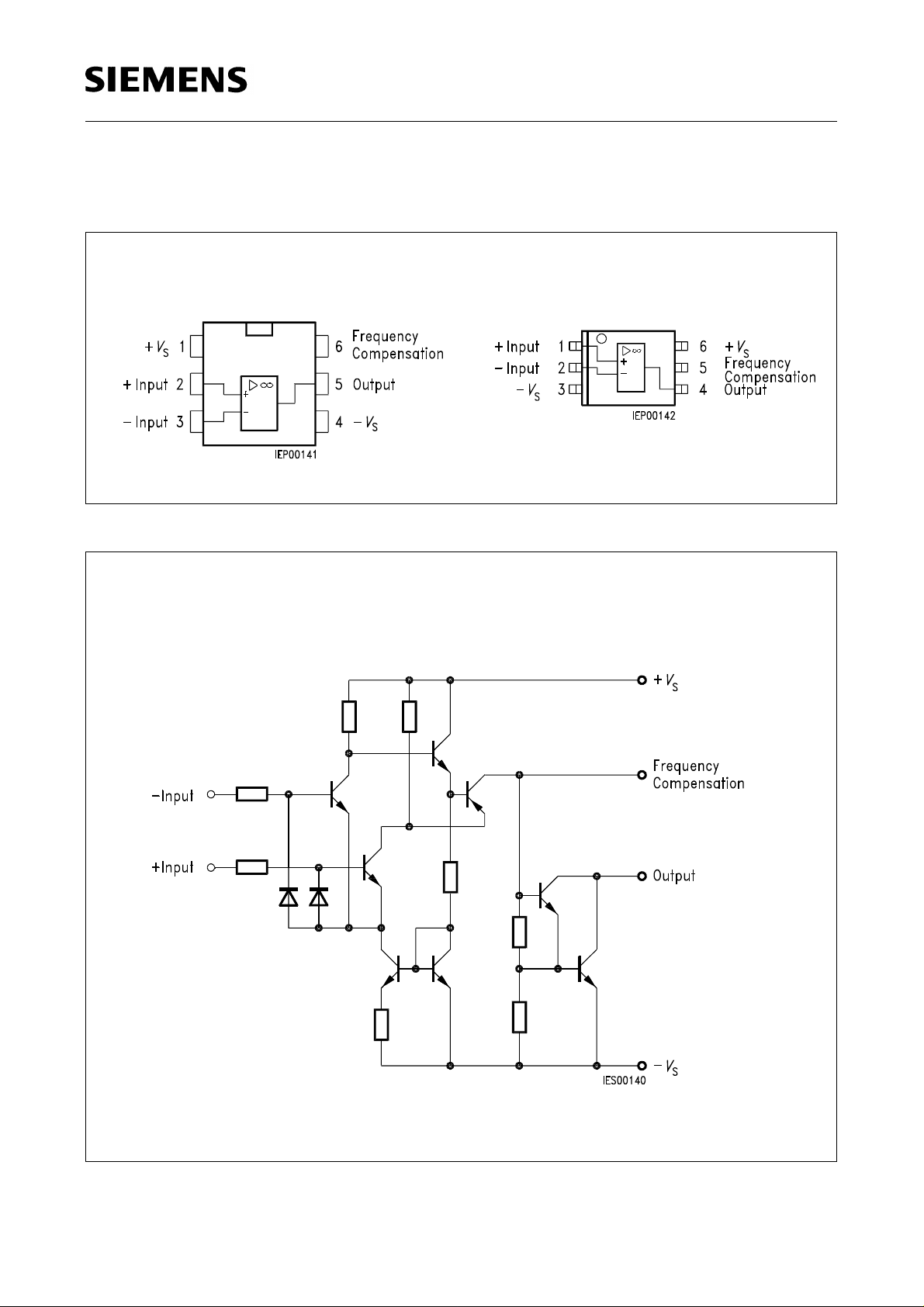
Pin Configurations
(top view)
TAA 762
TAA 765
TAA 762 A
TAA 765 A
TAA 762 G
TAA 765 G
Circuit Diagram
Semiconductor Group 2
Page 3
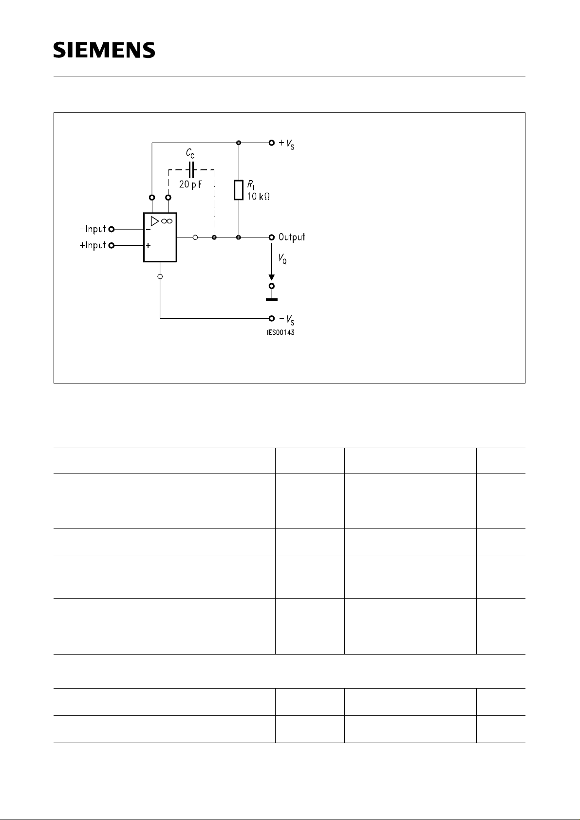
TAA 762
TAA 765
C
= output frequency compensation;
C
R
= load resistance (collector resistance)
L
Connection Diagram
Absolute Maximum Ratings (TAA 762)
Parameter Symbol Limit Values Unit
Supply voltage
Output current
Differential input voltage
Junction temperature
Storage temperature range
V
I
V
T
T
S
Q
ID
j
stg
± 18 V
70 mA
± V
S
150
– 55 to 125
V
°C
°C
Thermal resistance
system - air TAA 762 A
TAA 762 G
R
R
th SA
th SA
115
200
K/W
K/W
Operating Range (TAA 762)
Supply voltage
Ambient temperature
V
T
Semiconductor Group 3
S
A
± 1.5 to ± 18 V
– 55 to 125 °C
Page 4
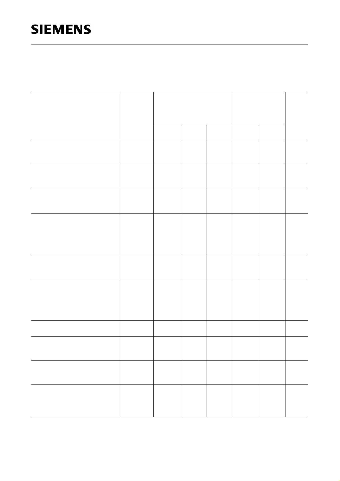
Characteristics (TAA 762)
V
= ± 5 V to ± 15 V; RL= 2 kΩ,
S
unless otherwise specified
TAA 762
TAA 765
Parameter Symbol Limit Values
T
= 25 °C
A
min. typ. max. min. max.
Open-loop supply
current consumption
Input offset voltage
R
= 50 Ω
G
Input offset current
Input current
I
V
I
I
S
IO
I
IO
–4 4 –6 6 mV
– 100 ± 50
1.5 2.5 2.5
100
0.3
0.7
Control range
V
= ± 15 V
S
R
= 620 Ω, VS = ± 15 V
L
V
= ± 15 V, f = 100 kHz
S
Input impedance
V
V
V
Z
Qpp
Qpp
Qpp
I
14.9
14.9
–14
– 12.5
± 10
200 kΩ
f = 1 kHz
Limit Values
T
= – 55
A
to 125 °C
– 300 300
1.0
14.8
14.8
–14
–12VV
Unit
mA
nA
µA
V
Open-loop voltage gain
f = 1 kHz
R
= 10 kΩ, f = 1 kHz
L
f = 1 MHz
Output reverse current
Common-mode
input voltage range
Common-mode
rejection
Supply voltage
rejection
G
= 100
V
G
G
G
I
V
k
k
V0
V0
V0
QR
IC
CMR
SVR
85 87
92
43
80 dB
dB
dB
15µA
–
V
S
+2
V
S
–2 –
V
S
+3
V
–3
S
V
80 85 75 dB
25 200 200 µV/V
Semiconductor Group 4
Page 5
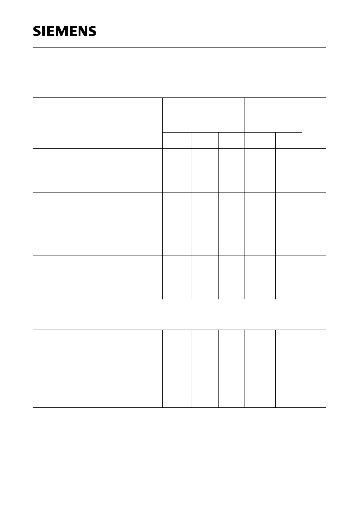
Characteristics (TAA 762) (cont’d)
V
= ± 5 V to ± 15 V; RL= 2 kΩ,
S
unless otherwise specified
TAA 762
TAA 765
Parameter Symbol Limit Values
T
= 25 °C
A
min. typ. max. min. max.
Temperature coefficient of
R
= 50
G
Ω
Temperature coefficient of
R
= 50
G
Slew rate of
Ω
V
Q
for
V
I
lO
IO
non-inverting operation
α
α
SR
VIO
IIO
6
0.3
9
25
1.5
(test circuit 1)
Slew rate of
inverting operation
V
Q
for
SR
18
(test circuit 2)
Noise voltage
V
n
3 µV
(in acc. with DIN 45 405;
referred to input;
R
= 2.5 kΩ)
S
Limit Values
T
= – 55
A
to 125 °C
25
1.5
Unit
µV/K
nA/K
V/µs
V/µs
Characteristics (TAA 762)
V
= ± 2V;RL= 2 kΩ
S
Input offset voltage
R
= 50 Ω
G
Input offset current
Input current
Open-loop voltage gain
V
I
I
G
IO
IO
I
V0
–4 4 –6 6 mV
–70
80 75 dB
f = 1 kHz
Semiconductor Group 5
0.2
70
0.5
– 200 200
0.8
nA
µA
Page 6
TAA 762
TAA 765
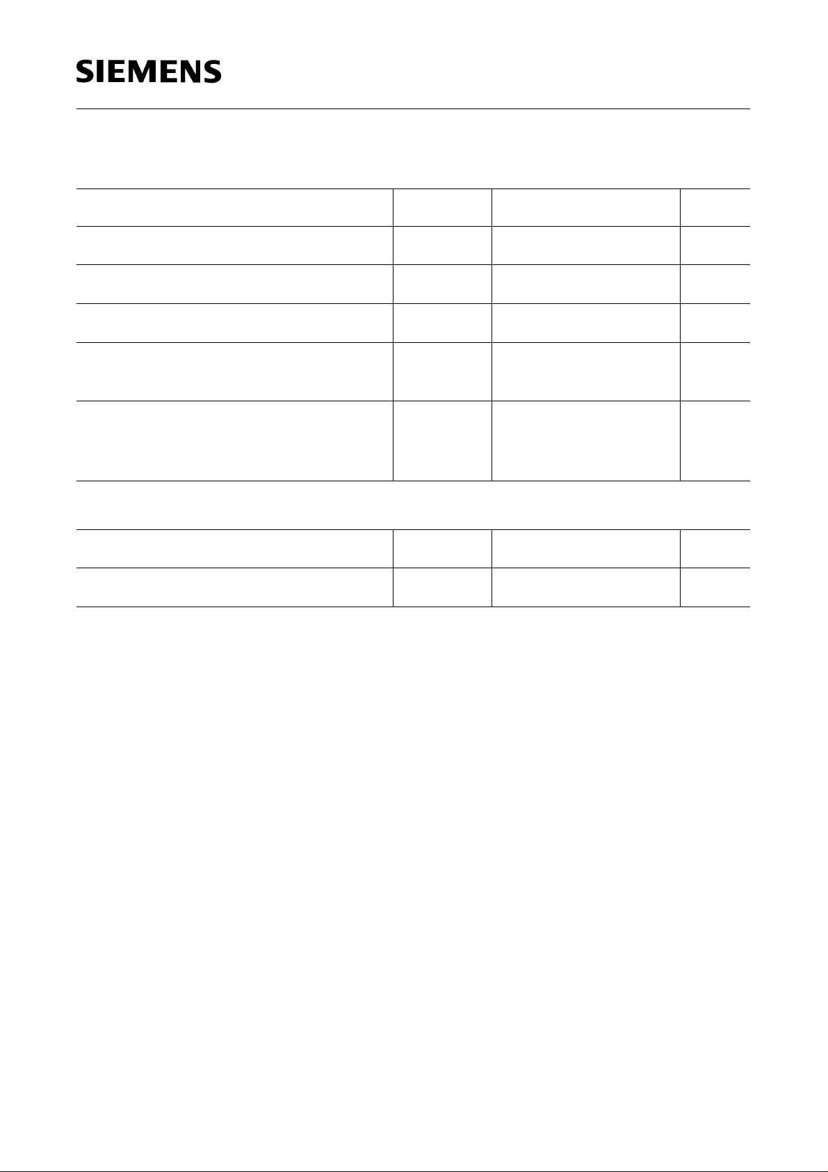
Absolute Maximum Ratings (TAA 765)
Parameter Symbol Limit Values Unit
Supply voltage
Output current
Differential input voltage
Junction temperature
Storage temperature range
Thermal resistance
system - air TAA 765 A
TAA 765 G
Operating Range (TAA 765)
Supply voltage
Ambient temperature
V
I
V
T
T
R
R
V
T
S
Q
ID
j
stg
th SA
th SA
S
A
± 18 V
70 mA
± V
S
150
– 55 to 125
115
200
V
°C
°C
K/W
K/W
± 1.5 to ± 18 V
– 25 to 85 °C
Semiconductor Group 6
Page 7
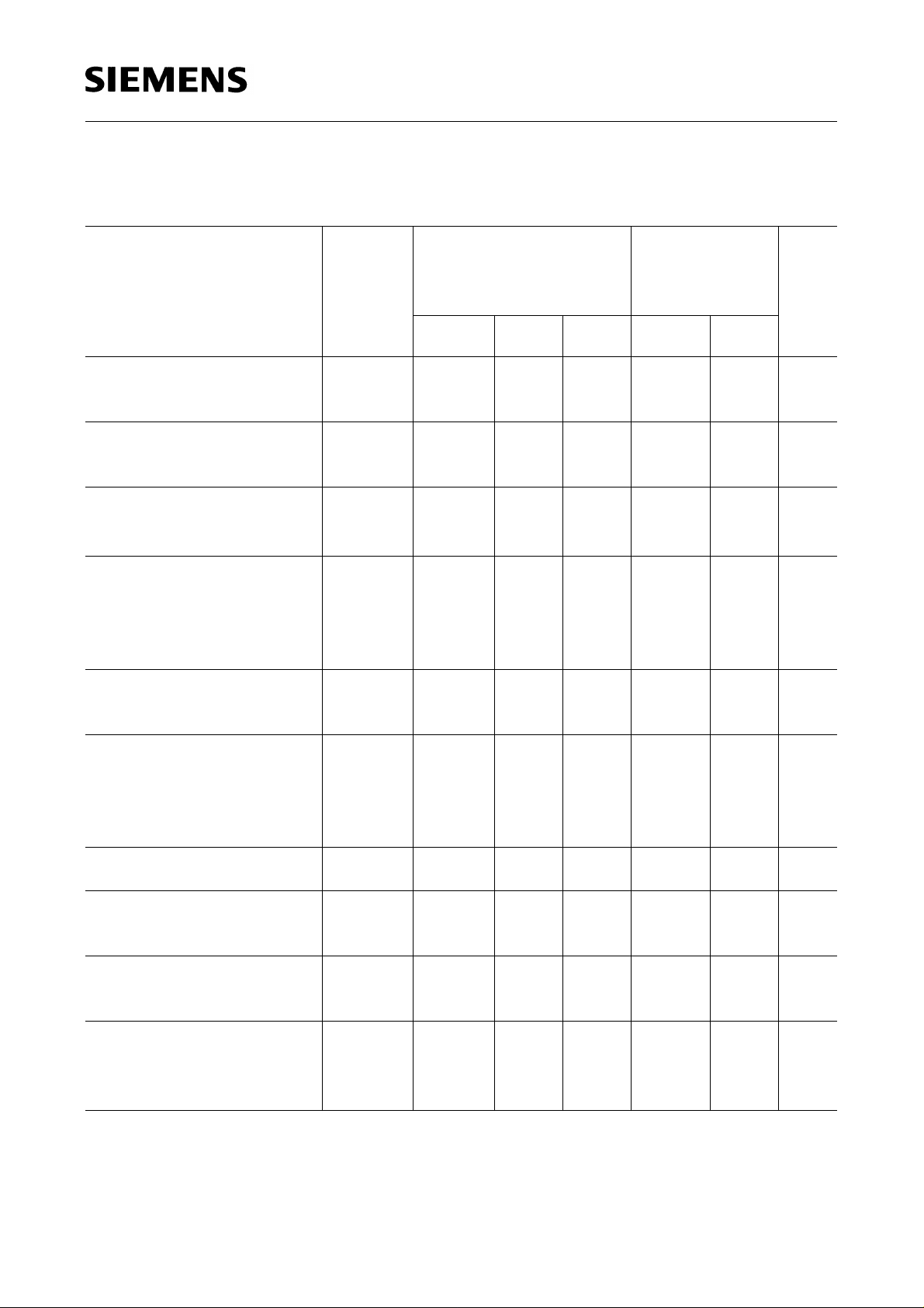
Characteristics (TAA 765)
V
= ± 5 V to ± 15 V; RL= 2 kΩ, unless otherwise specified
S
TAA 762
TAA 765
Parameter Symbol Limit Values
T
= 25 °C
A
min. typ. max. min. max.
Open-loop supply
current consumption
Input offset voltage
R
= 50 Ω
G
Input offset current
Input current
I
V
I
I
S
IO
I
IO
– 5.5 5.5 – 7 7 mV
– 200 ± 80
1.5 2.5 2.5 mA
0.5
Control range
V
= ± 15 V
S
R
= 620 Ω, VS = ± 15 V
L
V
= ± 15 V, f = 100 kHz
S
Input impedance
V
V
V
Z
Qpp
Qpp
Qpp
I
14.9
14.9
± 10
200 kΩ
f = 1 kHz
200
0.8
–14
– 12.5
Limit Values
T
= – 25
A
to 85 °C
– 300 300
1.0
14.8
14.8
–14
–12VV
Unit
nA
µA
V
Open-loop voltage gain
f = 1 kHz
R
= 10 kΩ, f = 1 kHz
L
f = 1 MHz
Output reverse current
Common-mode
input voltage range
Common-mode
rejection
Supply voltage
rejection
G
= 100
V
G
G
G
I
V
k
k
V0
V0
V0
QR
IC
CMR
SVR
80 85
90
43
80 dB
dB
dB
10 20 µA
–
V
+2
S
V
–2 –
S
V
+3
S
V
–3
S
V
75 83 75 dB
25 200 200 µV/V
Semiconductor Group 7
Page 8
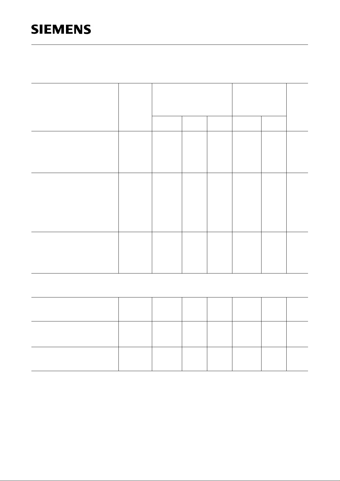
Characteristics (TAA 765) (cont’d)
V
= ± 5 V to ± 15 V; RL= 2 kΩ, unless otherwise specified
S
TAA 762
TAA 765
Parameter Symbol Limit Values
T
= 25 °C
A
min. typ. max. min. max.
Temperature coefficient of
R
= 50
G
Ω
Temperature coefficient of
R
= 50
G
Slew rate of
Ω
V
Q
for
V
I
IO
non-inverting operation
α
lO
VIO
α
VIO
SR
6
0.3
9
(test circuit 1)
Slew rate of
inverting operation
V
Q
for
SR
18
(test circuit 2)
Noise voltage
V
n
3 µV
(in acc. with DIN 45 405;
referred to input;
R
= 2.5 kΩ)
S
25
1.5
Limit Values
T
= – 25
A
to 85 °C
25
1.5
Unit
µV/K
nA/K
V/µs
V/µs
Characteristics (TAA 765)
V
= ± 2V;RL= 2 kΩ
S
Input offset voltage
R
= 30 Ω
G
Input offset current
Input current
Open-loop voltage gain
f = 1 kHz
V
I
I
G
IO
I
IO
V0
– 6 6 – 7.5 7.5 mV
– 150
0.2
150
0.6
– 200 200
0.8
nA
µA
75 75 dB
Semiconductor Group 8
Page 9
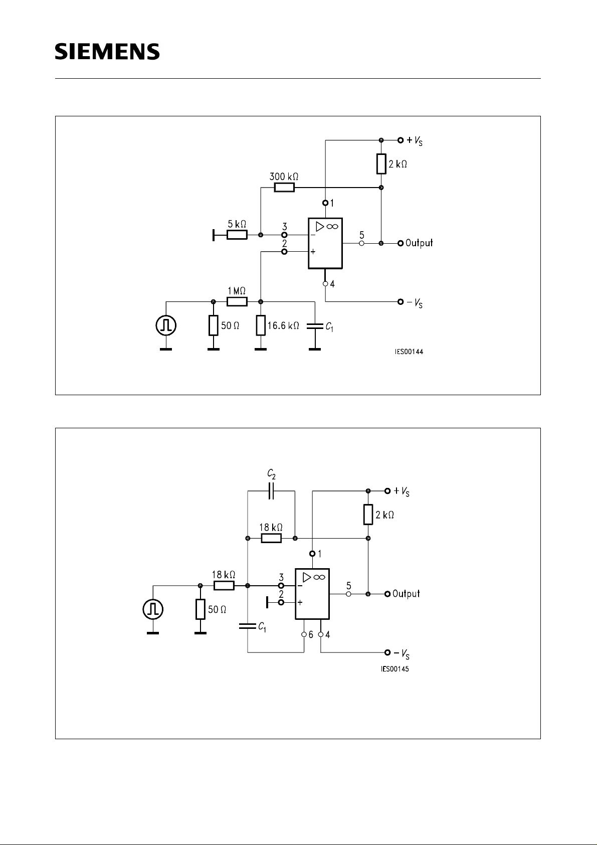
TAA 762
TAA 765
C1 for min. overshoot (approx. 22 pF)
Test Circuit 1 for Slew Rate (non-inverting operation)
C2 causes a frequency-dependent compensation to reduce rise times (approx. 390 pF)
C1 for min. overshoot (approx. 3.9 pF)
Test Circuit 2 for Slew Rate (inverting operation)
Semiconductor Group 9
Page 10
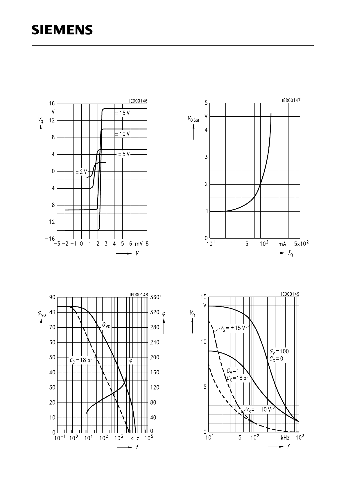
TAA 762
TAA 765
Transfer Characteristic
Output Voltage versus Input Voltage
V
= parameter, RL= 2 kΩ
S
Saturation Voltage versus
Output Current
T
= 25 °C
A
Open-Loop Voltage Gain and
Phase versus Frequency
V
= ± 15 V; RL = 2 kΩ
S
Frequency Dependence of Large
Signal Modulation Output Voltage
versus Frequency
Semiconductor Group 10
Page 11
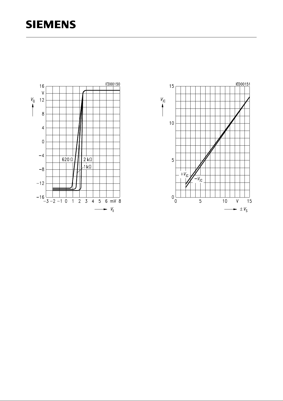
TAA 762
TAA 765
Transfer Characteristic
Output Voltage versus Input Voltage
V
= ± 15 V; RL= parameter
S
Common-Mode Voltage Range
Common-Mode Input
Voltage versus Supply Voltage
Semiconductor Group 11
Page 12
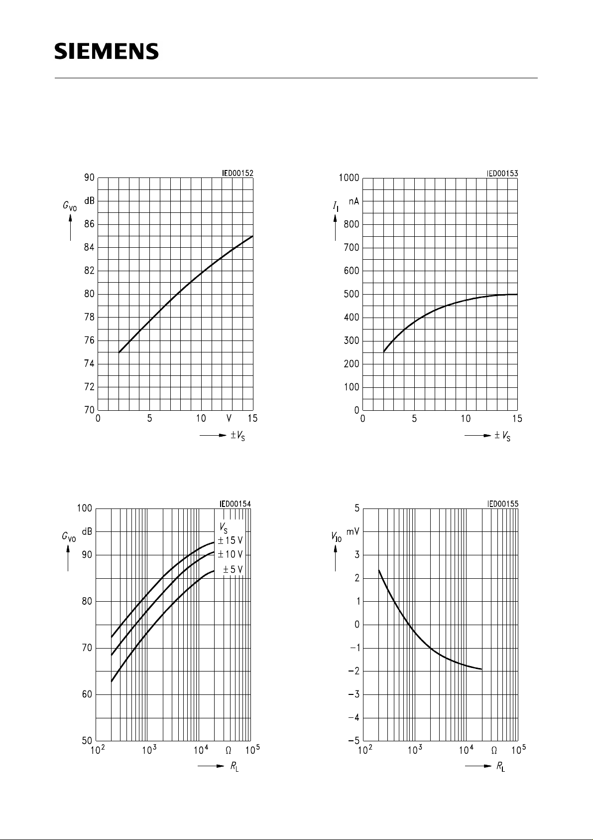
TAA 762
TAA 765
Open-Loop Voltage Gain versus
Supply Voltage
T
= 25 °C, RL= 2 kΩ
A
Input Current versus
Supply Voltage
Open-Loop Voltage Gain versus
Load Resistance
T
= 25 °C
A
Input Offset Voltage versus
Load Resistance
V
= ± 15 V
S
Semiconductor Group 12
Page 13
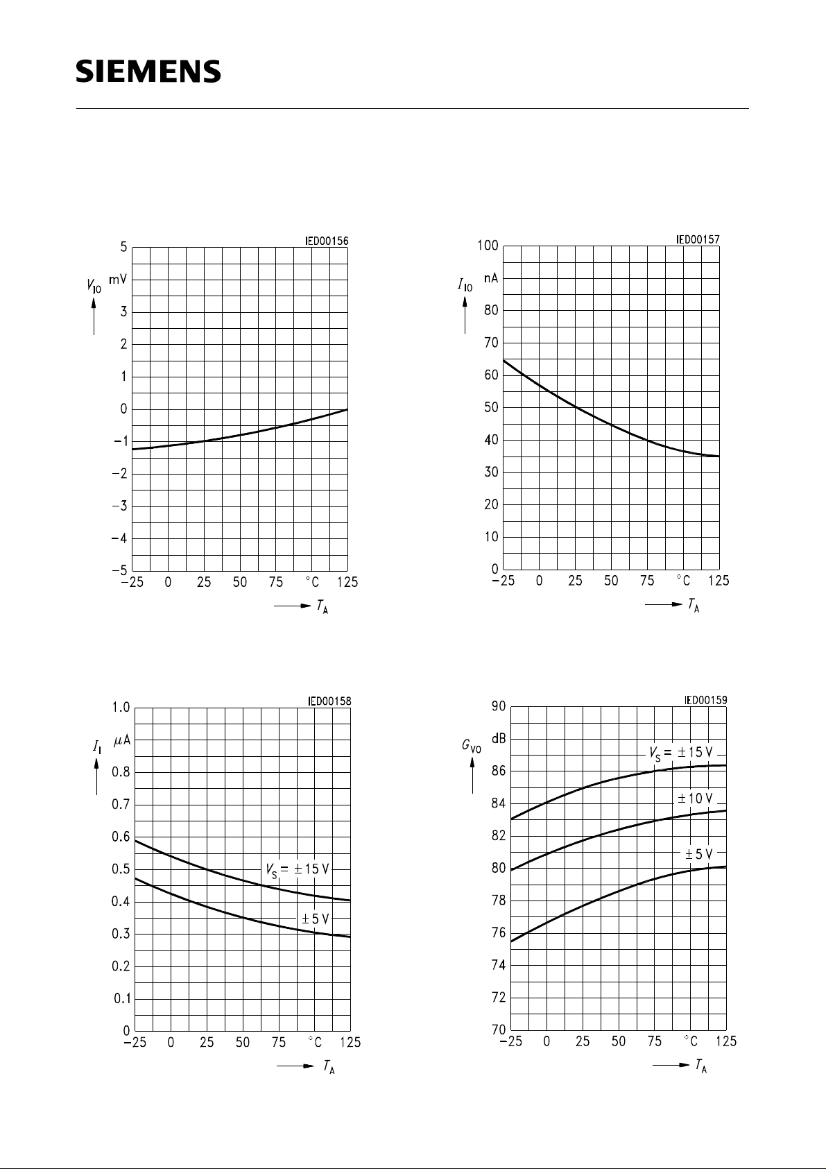
TAA 762
TAA 765
Input Offset Voltage versus
Ambient Temperature
R
= 2 kΩ; VS = ± 15 V
L
Input Offset Current versus
Ambient Temperature
R
= 2 kΩ; VS = ± 15 V
L
Input Current versus
Ambient Temperature
R
= 2 kΩ
L
Open-Loop Voltage Gain versus
Ambient Temperature
R
= 2 kΩ; f = 1 kHz
L
Semiconductor Group 13
 Loading...