

Page 1

Single PNP-Operational Amplifiers
Bipolar IC
Features
● PNP input
● Supply voltage range between 3 V and 36 V
● Low current consumption, 0.25 mA typ.
● Extremely large control range
● Low output saturation voltage, almost
independent of load current
● Output current up to 70 mA (100 mA max.)
● Wide common-mode range
● Wide operating temperature range (TAF 1453)
● Open collector output
Applications
TAE 1453
TAF 1453
P-DSO-6-1
● Amplifier
● Level converter
● Driver
● Zero voltage switch
● Comparator
Type Ordering Code Package
TAE 1453 G Q67000-A2106 P-DSO-6-1 (SMD)
TAF 1453 G Q67000-A2209 P-DSO-6-1 (SMD)
These operational amplifiers are circuits for universal applications having a PNP-input
differential stage and an open collector output. Apart from one resistor, only active
components are used. The integrated regulator provides for all parameters a large
degree of independence from the supply voltage.
Semiconductor Group 1 01.96
Page 2
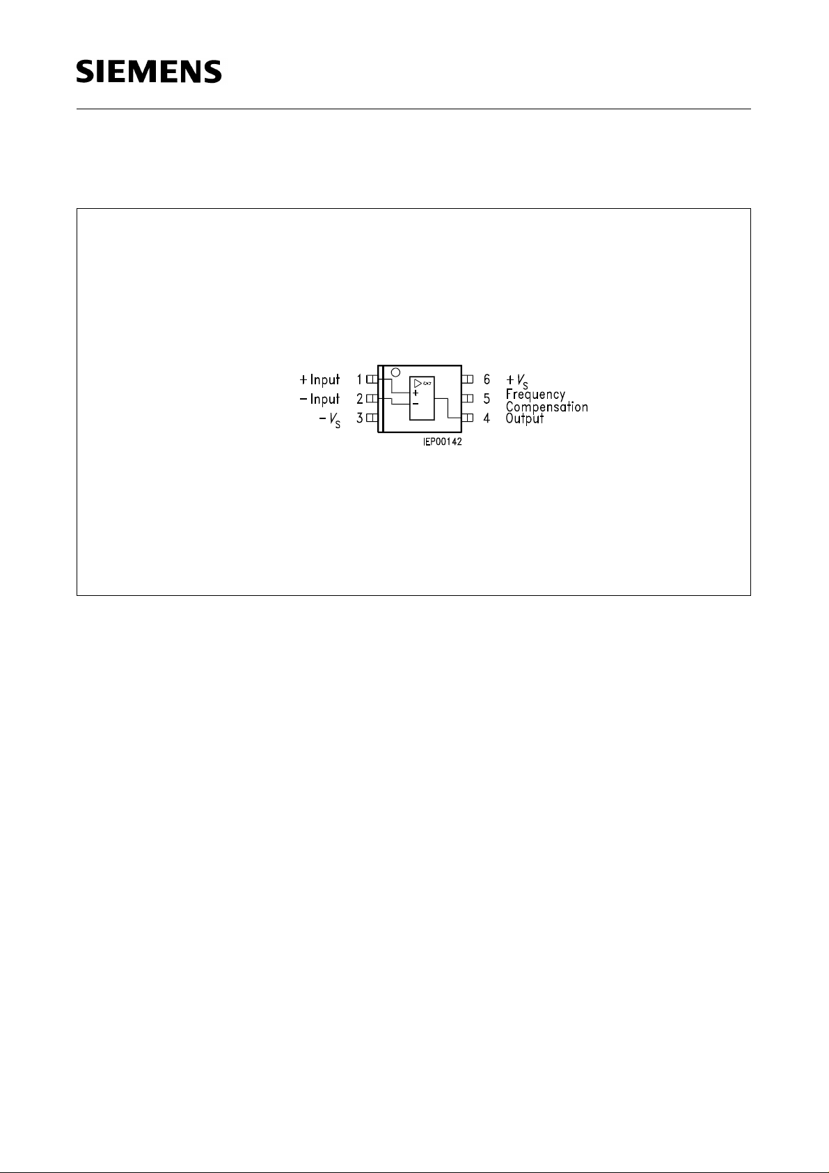
Pin Configurations
(top view)
TAE 1453
TAF 1453
TAE 1453 G
TAF 1453 G
Semiconductor Group 2
Page 3
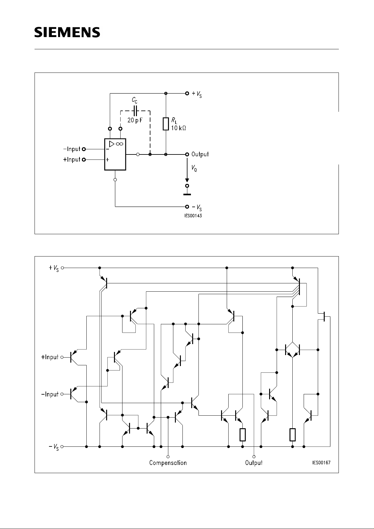
C
= output frequency
C
compensation (if required);
R
= load resistance
L
(collector resistance)
TAE 1453
TAF 1453
Connection Diagram
Circuit Diagram
Semiconductor Group 3
Page 4
TAE 1453
TAF 1453
Absolute Maximum Ratings (TAE 1453 G)
Parameter Symbol Limit Values Unit
Supply voltage V
Output current
Differential input voltage
Junction temperature
Storage temperature range
I
V
T
T
Thermal resistance
system - air TAE 1453 G
R
Operating Range (TAE 1453 G)
Supply voltage
Ambient temperature
V
T
S
Q
ID
j
stg
th SA
S
A
± 18 V
100 mA
± V
S
150
– 55 to 150
V
°C
°C
200 K/W
± 2 to ± 18
V
(± 1.5 V with
slightly increased
offset voltage)
– 25 to 85 °C
Characteristics (TAE 1453 G)
V
= ± 5Vto±15 V; RL = 10 kΩ, unless otherwise specified
S
Parameter Symbol Limit Values
T
= 25 °C
A
min. typ. max. min. max.
Open-loop
I
S
0.25 0.4 0.45 mA
current consumption
Input offset voltage,
Input offset current
Input current
R
= 50 Ω V
G
IO
I
IO
I
I
– 5.5 5.5 – 7 7 mV
–15
40
15
150
Limit
Values
T
= – 25
A
to 85 °C
– 100
100
200
Unit
nA
nA
Semiconductor Group 4
Page 5

Characteristics (TAE 1453 G) (cont’d)
V
= ± 5Vto±15 V; RL = 10 kΩ, unless otherwise specified
S
TAE 1453
TAF 1453
Parameter Symbol Limit Values
T
= 25 °C
A
min. typ. max. min. max.
Control range
R
= 2 kΩ, VS = ± 15 V
L
R
= 620 Ω, VS = ± 15 V
L
R
= 2 kΩ, VS = ± 15 V,
L
V
V
V
Q pp
Q pp
Q pp
14.9
14.9
10
– 14.7
– 14.5
–10
f = 100 kHz
Input impedance,
Open-loop voltage gain
Output reverse current
Common-mode input
voltage range
f = 1 kHz Z
G
I
V
I
QR
IC
V0
200 kΩ
78 85 78 dB
10 20 µA
– V
S
– 0.2
V
– 1.8
Limit
Unit
Values
T
= – 25
A
to 85 °C
14.9
14.9
– 14.7
– 14.4VV
V
V
S
–
V
S
S
V
– 2.0
Common-mode rejection
Supply voltage rejection
G
= 100
V
Temperature coefficient of
R
= 50 Ω
G
Temperature coefficient of
R
= 50 Ω
G
Slew rate
for non-inverting operation
Slew rate
for inverting operation
1)
C
= 15 pF
k
I
V
IO
IO
k
CMR
k
SVR
α
α
SR
SR
IIO
VIO
75 80 75 dB
25 100 120 µV/V
0.1
6
6
6
3
3
11
10
nA/K
µV/K
V/µs
V/µs
1)
1)
Semiconductor Group 5
Page 6

Characteristics (TAE 1453 G)
V
= ± 2.5 V, RL = 10 kΩ
S
TAE 1453
TAF 1453
Parameter Symbol Limit Values
T
= 25 °C
A
Limit
Values
T
= – 25
A
Unit
to 85 °C
min. typ. max. min. max.
Input offset voltage,
Input offset current
Input current
Open-loop voltage gain
R
= 50 Ω V
G
I
I
G
IO
I
IO
V0
– 6 6 – 7.5 7.5 mV
–15
40
15
150
– 100
100
200nAnA
70 70 dB
Absolute Maximum Ratings (TAF 1453 G)
Parameter Symbol Limit Values Unit
Supply voltage
Output current
V
I
S
Q
± 18 V
100 mA
Differential input voltage
Junction temperature
Storage temperature range
Thermal resistance
system - air TAF 1453 G
Operating Range (TAF 1453 G)
Supply voltage
Ambient temperature
V
T
T
R
V
T
ID
j
stg
th SA
S
A
± V
S
150
– 55 to 125
V
°C
°C
200 K/W
± 2 to ± 18
V
(± 1.5 V with
slightly increased
offset voltage)
– 55 to 125 °C
Semiconductor Group 6
Page 7

Characteristics (TAF 1453 G)
V
= ± 5Vto±15 V; RL = 10 kΩ, unless otherwise specified
S
TAE 1453
TAF 1453
Parameter Symbol Limit Values
T
= 25 °C
A
min. typ. max. min. max.
Open-loop current consumption
I
S
0.25 0.35 0.45 mA
(Output in H state)
Input offset voltage,
Input offset current
Input current
R
= 50 Ω V
G
IO
I
IO
I
I
–4 4 –6 6 mV
–10
40
10
100
Control range
R
= 2 kΩ, VS = ± 15 V
L
R
= 620 Ω, VS = ± 15 V
L
R
= 2 kΩ, VS = ± 15 V, f = 100 kHz
L
Input impedance,
f = 1 kHz Z
V
V
V
Q pp
Q pp
Q pp
I
14.9
14.9
10
– 14.7
– 14.5
–10
200 kΩ
Limit
Values
T
= – 55
A
to 125 °C
–75 75
150nAnA
14.9
14.9
– 14.7
– 14.4VV
Unit
V
Open-loop voltage gain
Output reverse current
Common-mode input
voltage range
Common-mode rejection
Supply voltage rejection
G
= 100
V
Temperature coefficient of
R
= 50 Ω
G
Temperature coefficient of
R
= 50 Ω
G
I
V
IO
IO
G
I
V
k
k
α
α
V0
QR
IC
CMR
SVR
IIO
VIO
80 85 75 dB
15µA
– V
S
– 0.2
V
S
– 1.5
V
–
S
+ 0.2
V
S
– 1.8
V
80 85 75 dB
25 100 100 µV/V
0.1
6
0.8
25
nA/K
µV/K
Semiconductor Group 7
Page 8

Characteristics (TAF 1453 G)
V
= ± 2.5 V, RL = 10 kΩ
S
TAE 1453
TAF 1453
Parameter Symbol Limit Values
T
= 25 °C
A
min. typ. max. min. max.
Slew rate
SR
6
for non-inverting operation
Slew rate
SR
6
for inverting operation
Input offset voltage, RG = 50 Ω V
Input offset current
Input current
Open-loop voltage gain
1)
C
= 15 pF
k
I
I
G
IO
IO
I
V0
–4 4 –6 6 mV
–50
40
50
100
75 70 dB
Limit
Values
T
= – 55
A
to 125 °C
2
2
12
11
–75 75
150nAnA
Unit
V/µs
V/µs
1)
1)
Semiconductor Group 8
Page 9

Typical Characteristics of Electrical Parameters
Load Characteristics
Output Saturation Voltage versus
Output Current
TAE 1453
TAF 1453
Output Saturation Voltage versus Output Current
Semiconductor Group 9
Page 10

Supply Current versus Supply Voltage
TAE 1453
TAF 1453
Input Current and Input Offset Current
versus Supply Voltage
Semiconductor Group 10
Page 11

Input Offset Voltage versus Supply Voltage
TAE 1453
TAF 1453
V
Behavior at Low Operating Voltages
IO
Input Offset Voltage versus Supply Voltage
Semiconductor Group 11
 Loading...