

TA8805F,TA1207F
r
r
y
t
y
r
TOSHIBA BIPOLAR LINEAR INTEGRATED CIRCUIT SILICON MONOLITHIC
TA8805F,TA1207F
FOR LCD TVS, PIF AND SIF SYSTEM
FEATURES
PIF circuit
• High input sensitivity
• 3-stage variable-gain PIF amplifier
• Output with black noise inverter (TA8805F)
• Output without black noise inverter (TA1207F)
• High-speed response peak AGC with dual time constant
• Reverse RF AGC output (Emitter follower type)
• Built-in AFT detection circuit with AFT mute
SIF circuit
• 4-stage SIF amplifier
• Quadrature-type detection circuit
• Use of a ceramic discriminator device makes the SIF circuit
adjustment-free
• Electronic volume control
• Built-in audio amplifier (output power : 30 mW (Typ.) )
Weight: 0.32 g(Typ.)
000707EBA1
• TOSHIBA is continually working to improve the quality and reliability of its products. Nevertheless, semiconductor devices in general
can malfunction or fail due to their inherent electrical sensitivity and vulnerability to physical stress. It is the responsibility of the
buyer, when utilizing TOSHIBA products, to comply with the standards of safety in making a safe design for the entire system, and
to avoid situations in which a malfunction or failure of such TOSHIBA products could cause loss of human life, bodily injury o
damage to property.
In developing your designs, please ensure that TOSHIBA products are used within specified operating ranges as set forth in the
most recent TOSHIBA products specifications. Also, please keep in mind the precautions and conditions set forth in the “Handling
Guide for Semiconductor Devices,” or “TOSHIBA Semiconductor Reliability Handbook” etc..
• The TOSHIBA products listed in this document are intended for usage in general electronics applications (computer, personal
equipment, office equipment, measuring equipment, industrial robotics, domestic appliances, etc.). These TOSHIBA products are
neither intended nor warranted for usage in equipment that requires extraordinarily high quality and/or reliability or a malfunction o
failure of which may cause loss of human life or bodily injury (“Unintended Usage”). Unintended Usage include atomic energ
control instruments, airplane or spaceship instruments, transportation instruments, traffic signal instruments, combustion control
instruments, medical instruments, all types of safety devices, etc.. Unintended Usage of TOSHIBA products listed in this documen
shall be made at the customer’s own risk.
• The products described in this document are subject to the foreign exchange and foreign trade laws.
• The information contained herein is presented only as a guide for the applications of our products. No responsibility is assumed b
TOSHIBA CORPORATION for any infringements of intellectual property or other rights of the third parties which may result from its
use. No license is granted by implication or otherwise under any intellectual property or other rights of TOSHIBA CORPORATION o
others.
• The information contained herein is subject to change without notice.
2001-02-26 1/17
TA8805F,TA1207F
BLOCK DIAGRAM
BLOCK DIAGRAM
(TA8805F)
(TA1207F)
2001-02-26 2/17
TERMINAL FUNCTION
TA8805F,TA1207F
PIN
No.
1 2 PIF AGC1
3 RF AGC Output
4 RF AGC Delay
PIN NAME FUNCTION INTERFACE
PIF AGC
2
This IC is adopted dual time constant
AGC circuit to
improve AGC responsibility.
To mute picture, connect to
GND
RF AGC output terminal.
(Emitter follower type)
Output current : 3 mA (Typ.)
Changing comparator
reference voltage adjusts RF AGC
delay point.
5 PIF VCC
6 7 PIF Input 1
PIF Input 2
8 PIF GND
Connect bypass capacitor between this
terminal and PIF GND with shortest
wiring.
PIF input terminal.
Input impedance 5 kΩ (Typ.)
Connect bypass capacitor between this
terminal and PIF VCC with shortest
wiring.
—
—
2001-02-26 3/17
TA8805F,TA1207F
PIN
No.
PIN NAME FUNCTION INTERFACE
9 SIF Input
10 SIF VCC
11 Volume
12 Audio Output
13 SIF GND
Connect B.P.F. between this
terminal and pin 23.
Connect bypass capacitor
between this terminal and SIF
GND with shortest wiring.
Control audio amp. gain.
(Control range 70 dB (Typ.) )
Audio signal output terminal.
(Output power : 30 mW (Typ.) )
Connect bypass capacitor between this
terminal and SIF VCC with shortest
wiring.
—
—
14 Audio Input
15 FM Det. Input
17 De-emphasis Audio signal output terminal.
Audio signal input terminal.
Input audio signal from pin 17 through
filter
Quadrature input terminal for FM
detection circuit.
Connect FM coil between this terminal
and pin 16.
Audio output is muted when this
terminal is connected to GND.
2001-02-26 4/17

PIN
No.
16 Limiter Output
18
Sync. Sepa. Sync. sepa. output and input terminal.
22
TA8805F,TA1207F
PIN NAME FUNCTION INTERFACE
Limiter output terminal.
Connect FM coil between this terminal
and pin 15.
Applying ceramic discriminator sets
this circuit to non-adjustable circuit.
19
Video Coil 1
20
Video Coil 2
21 AFT Coil
23 Video Output Video signal output terminal.
Connect video detection coil.
Connect AFT detection coil.
AFT output is defeated when this
terminal connected to GND.
24 AFT Output
AFT detector output terminal based on
double balanced multiplier.
AFT output is muted when AFT coil
terminal is connected to GND.
2001-02-26 5/17
TA8805F,TA1207F
MAXIMUM RATINGS
CHARACTERISTIC SYMBOL RATING UNIT
Power Supply Voltage VCC 8 V
Power Dissipation PD (Note) 500 mW
Operating Temperature T
Storage Temperature T
(Ta = 25°C)
−20~65 °C
opr
−55~150 °C
stg
Note: When using the device at above Ta = 25°C, decrease the power dissipation by 4 mW for each increase of
1°C.
RECOMMENDED POWER SUPPLY
PIN
No.
5 PIF VCC 3.5 4.5 7.5 V
9 SIF VCC 3.5 4.5 7.5 V
ELECTRIC CHARACTERISTICS
PIN NAME MIN TYP. MAX UNIT
(Unless otherwise specified, V
= 4.5 V, Ta = 25°C)
CC
DC CHARACTERISTICS
PIN
No.
1 AGC1 1st AGC filter — 4.2 —
2 AGC2 2nd AGC filter — 4.2 —
3 RF AGC RF AGC output 3.6 3.8 4.0
4 RF AGC delay RF AGC delay — — —
5 PIF VCC PIF VCC — 4.5 —
6 PIF input 1 IF input 2.5 2.9 3.2
7 PIF input 2 IF input 2.5 2.9 3.2
8 PIF GND PIF GND — 0 —
9 SIF input SIF input 4.3 4.45 4.6
10 SIF VCC SIF VCC — 4.5 —
11 Volume control Audio volume control 2.0 2.2 2.4
12 Audio output Audio output 0.9 1.3 1.7
13 SIF GND SIF GND — 0 —
14 Audio input Audio input — — 0.5
15 FM det. Input FM det. Output 3.5 3.7 3.9
16 Limiter output SIF limiter output 2.55 2.75 2.95
17 De-emphasis Audio de-emphasis 1.15 1.45 1.75
18 Sync. sepa. Output Sync. sepa. signal output — — —
19 Video coil 1 PIF carrier output 4.05 4.15 4.25
20 Video coil 2 PIF carrier output 4.05 4.15 4.25
21 AFT coil Connecting AFT coil 4.35 4.45 4.55
22 Sync. sepa. Input Sync. sepa. signal output — — —
23 Video output 1 Video signal output 1.40 1.85 2.30
24 AFT output AFT output 1.3 1.8 3.2
PIN NAME FUNCTION MIN TYP. MAX UNIT
V
2001-02-26 6/17

TA8805F,TA1207F
AC CHARACTERISTICS
(Unless otherwise specified, V
= 4.5 V, Ta = 25°C)
CC
PIF circuit
TEST
CHARACTERISTIC SYMBOL
Power Supply Current at No Signal I
Output Signal Voltage VD 2 (Note 1) 0.7 1.0 1.3 V
PIF Input Signal Voltage Sensitivity V
Maximum input Signal Voltage V
−3 dB Video Band Width BW 2 (Note 4) 5 6.5 — MHz
Dependence of Output Signal Voltage
On Power Supply Voltage
Deferential Gain DG — 5 10 %
Deferential Phase DP
Signal-Noise Ratio S / N 2 (Note 7) 40 45 — dB
Intermodulation IM 4 (Note 8) 30 35 — dB
Suppression of Picture Career CR 2 (Note 9) 45 50 — dB
Sync. Voltage Level Vp 2
Output Voltage at No Signal Vz 2 (Note 10) 1.6 2.0 2.4 V
Black Noise Inverter Level V
Black Noise Clamp Level V
AFT Control Steepness ∆f / ∆V 10 20 30 kHz / V
AFT maximum Output Voltage V
AFT minimum Output Voltage V
AFT Mute Voltage V
PIF Amp. Input Impedance
Video Signal Output Impedance P
Video Amp. Output Impedance R
PIF
i MIN
i MAX
V
/ VCC 2 (Note 5) — ±5 — % / V
D
BTH
BCL
MAX
MIN
MUTE
RIN 2 — — 5 — kΩ
C
IN
OUT
OUT
CIR-
CUIT
1 — — 11 16 mA
2 (Note 2) — 43 50 dBµV
2 (Note 3) 95 114 — dBµV
3 (Note 6)
87.5%AM, standard color-bar
signal
0.4 0.6 0.8
2
4.0 4.3 4.5
— 0.3 0.5
2 — — 3.8 — pF
2 Load : 100 kΩ / 100 kΩ
2 — — 200 — Ω
2 — — 200 — Ω
CONDITION MIN TYP. MAX UNIT
p-p
— 4 8 °
0.6 0.8 1.0 V
(Note 11)
(TA8805F)
1.0 1.2 1.4
2.1 2.25 2.4
V
V
2001-02-26 7/17

TA8805F,TA1207F
SIF circuit
TEST
CHARACTERISTIC SYMBOL
Power Supply Current at No Signal I
Output Signal Voltage VOD 2 (Note 12) 120 150 180 mV
SIF Input Signal Voltage Sensitivity V
Total Harmonic Distortion THD (DET) 2 (Note 14) — 0.4 1.0 %
AM Rejection AMR 5 (Note 15) 30 45 — dB
Signal-Noise Ratio S / N DET 2 (Note 16) 50 65 — dB
−3 dB Bandwidth BW − 3dB 2 (Note 17) 180 230 — kHz
Dependence of Output Signal Voltage
On Power Supply Voltage
Audio Amp. Voltage Gain GAF 2 (Note 19) 7.0 10.0 13.0 dB
Audio Amp. Total Harmonic Distortion THDAF 2 (Note 20) — 0.3 1.0 %
Audio Amp. Maximum Attenuation ATT
Audio Amp. S / N S / NAF 2 (Note 22) 40 50 — dB
Audio Amp. Output Power PO 2 (Note 23) 15 30 — mW
SIF
LIM
V
/ VCC 2 (Note 18) —— 10 15 % / V
OD
MAX
Sync. sepa. circuit
CIR-
CUIT
1 — — 6 11 mA
2 (Note 13) 30 35 40 dBµV
2 (Note 21) 60 70 — dB
CONDITION MIN TYP. MAX UNIT
rms
CHARACTERISTIC SYMBOL
Sync. Sepa. input Voltage V
Sync. Sepa. Minimum Output Voltage V
Sync. Sepa. Maximum Output Voltage V
SYNC.IN
SYNC.MIN
SYNC.MAX
TEST
CIR-
CUIT
2 — 1.8 2.1 3.0 V
2 0 0.2 0.4 V
2
Load : 47 kΩ
CONDITION MIN TYP. MAX UNIT
4.3 4.5 — V
2001-02-26 8/17

TEST CONDITION
<PIF circuit>
Note 1: Output signal voltage
PIF input : f
Measure output video signal voltage.
Note 2: PIF input signal voltage sensitivity
PIF input : f
Measure output video signal voltage (that voltage is 0 dB). Lower input signal voltage gradually,
measure input PIF signal voltage when output video signal voltage is −3 dB.
Note 3: Maximum input signal voltage
PIF input : f
Measure output video signal voltage (that voltage is 0 dB). Raise input signal voltage gradually,
measure input PIF signal voltage when output video signal voltage is +3 dB
Note 4: −3 dB video band width
(1) PIF input :
f
= 58.75 MHz, 84 dBµV, CW
o
Measure IF AGC voltage and supply that voltage from external source.
(2) Input following composite signals to the PIF input :
SG : 1 58.75 MHz, 84 dBµV (frequency : fixed)
SG : 2 58.65~45 MHz, 64 dBµV (frequency : variable)
Monitor spectrum of output signal at pin 24. Change frequency of SG : 2, measure frequency of
SG : 2, when video output signal is −3 dB.
Difference between that frequency and 58.75 MHz is −3 dB band width.
Note 5: Dependence of output signal voltage on power supply voltage
PIF input : f
Measure the output video signal voltage when power supply voltage are 3.5 V and 5.5 V. (4.5 ± 1.0 V)
Compare those voltage and the output video signal voltage when power supply voltage is 4.5 V.
Note 6: Deferential gain / Deferential phase
PIF input : f
free
Measure deferential gain and deferential phase.
= 58.75 MHz, 87.5%AM, 84 dBµV, standard TV signal (V / S = 10 : 4 Ramp)
o
= 58.75 MHz, fm = 15.75 kHz, 30%AM, 84 dBµV
o
= 58.75 MHz, fm = 15.75 kHz, 30%AM, 84 dBµV
o
= 58.75 MHz, 87.5%AM, 84 dBµV, standard TV signal (V / S = 10 : 4 Ramp)
o
= 58.75 MHz, 87.5%AM, 84 dBµV, standard TV signal (V / S = 10 : 4 Ramp) IF AGC :
o
TA8805F,TA1207F
2001-02-26 9/17

Note 7: Signal-noise ratio
(1) PIF input : f
= 58.75 MHz, fm = 15.75 kHz, 30%AM, 84 dBµV
o
Measure IF AGC voltage and supply that voltage from external source.
(2) Measure output video signal voltage. : V
(3) PIF input :
= 58.75 MHz, 84 dBµV, CW
fo
Measure output video signal voltage. : V
Signal-noise ratio is calculated by following equality.
Signal-noise ratio = 20
ogl
(V1 × 6 / V2) [dB]
Note 8: Intermodulation
(1) PIF input : f
= 58.75 MHz, 84 dBµV, CW
o
Supply DC voltage to IF AGC from external source to fix IF AGC voltage.
(2) PIF input : following composite signals
f
= 58.75 MHz, 84 dBµV, CW
o
f
= 55.17 MHz, 74 dBµV, CW Input
c
f
= 54.25 MHz, 74 dBµV, CW
s
Measure the difference of signal level at pin 24 920 kHz component and 3.58 MHz component
(Chroma sub-carrier).
Note 9: Suppression of picture career
(1) PIF input : f
= 58.75 MHz, fm = 15.75 kHz, 78%AM, 84 dBµV
o
Measure IF AGC voltage and supply that voltage from external source.
(2) Measure output video signal voltage. : V
(3) PIF input : f
= 58.75 MHz, 84 dBµV, CW
o
Measure signal level of 58.75 MHz component at pin 24. : V
Signal-noise ratio is calculated by following equality.
Suppression of picture career = 20 ×
Note 10: Output voltage at no signal
PIF input : no input IF AGC : GND
Measure output video signal DC voltage.
Note 11: Black noise inverter level / Black noise clamp level
PIF input : f
= 58.75 MHz, fm = 15.75 kHz, 78%AM, 84 dBµV
o
Supply 0 V to IF AGC from external source. Raise that voltage gradually, measure black noise
inverter level.
TA8805F,TA1207F
1
2
1
2
ogl
(V1 / V2) [dB]
2001-02-26 10/17

<SIF circuit>
Note 12: Output signal voltage
SIF input : f
= 4.5 MHz, fm = 400 Hz, 25 kHz / devi, 84 dBµV
o
Measure output audio signal voltage.
Note 13: SIF input signal voltage sensitivity
SIF input : f
= 4.5 MHz, fm = 400 Hz, 25 kHz / devi, 84 dBµV
o
Measure output audio signal voltage (that voltage is 0 dB). Lower input SIF signal voltage gradually,
measure input SIF signal voltage when output audio signal voltage is −3 dB.
Note 14: Total harmonic distortion
SIF input : f
= 4.5 MHz, fm = 400 Hz, 7.5 kHz / devi, 84 dBµV
o
Note 15: AM Rejection
SIF input :
(1) FM : f
(2) AM : f
= 4.5 MHz, fm = 400 Hz, 25 kHz / devi, 84 dBµV
o
= 4.5 MHz, fm = 400 Hz, 30%AM, 84 dBµV
o
Measure difference of output audio signal voltage between (1) and (2).
Note 16: Signal-noise ratio
SIF input : f
Measure audio signal output voltage. : V
SIF input : f
Measure audio signal output voltage. : V
= 4.5 MHz, fm = 400 Hz, 25 kHz / devi, 84 dBµV
o
[mV
1
= 4.5 MHz, fm = 400 Hz, 25 kHz / devi, 84 dBµV
o
[mV
2
rms
rms
]
]
Signal-noise ratio is calculated by following equality.
Signal-noise ratio = 20
ℓog
(V1 / V2) [dB]
Note 17: −3 dB bandwidth
SIF input : f
= 4.5 MHz, fm = 400 Hz, 25 kHz / devi, 84 dBµV
o
Measure audio signal output voltage (that voltage is 0 dB). Then change input signal frequency,
measure bandwidth that audio signal output voltage within −3 dB.
Note 18: Dependence of output signal voltage on power supply voltage
SIF input : f
= 4.5 MHz, fm = 400 Hz, 25 kHz / devi, 84 dBµV
o
Measure the audio signal output voltage when power supply voltage are 3.5 V and 5.5 V. (4.5 ± 1.0 V)
Compare those voltage and audio signal output voltage when power supply voltage is 4.5 V.
Note 19: Audio amp. voltage gain
Audio input : f = 1 kHz, V
= 100 mV
IN
, Pin 11 : VCC
rms
TA8805F,TA1207F
2001-02-26 11/17

Note 20: Audio amp. total harmonic distortion
Audio input : f = 1 kHz, V
= 100 mV
IN
Note 21: Audio amp. maximum attenuation
Audio input : f = 1 kHz, V
Audio output (Pin 11: V
CC
IN
) = V
= 100 mV
Audio output (Pin 11: GND) = V
ATT
= 20 ℓog (V
max
max
/ V
min
Note 22: Audio amp. S / N
(1) Audio input : f = 1 kHz, V
Measure audio output : V
(2) Audio input : No signal
Measure audio output : V
S / N = 20 ℓog (V1 / V2) [dB]
Note 23: Audio amp. output power
Audio input : f = 1 kHz, Pin 11 = V
Raise input signal voltage gradually, measure output signal voltage when THD is 5%.
P
= V2 / 8 [W]
o
, Pin 11 = VCC
rms
rms
max
min
)
= 100 mVrms, Pin 11 = VCC
IN
1
2
, Load = 8Ω
CC
TA8805F,TA1207F
2001-02-26 12/17

TA8805F,TA1207F
TEST CIRCUIT 1
TEST CIRCUIT 2
(DC CHARACTERISTIC)
(AC CHARACTERISTIC)
2001-02-26 13/17

TA8805F,TA1207F
TEST CIRCUIT 3
TEST CIRCUIT 4
(DG, DP)
(INTERMODULA T ION)
TEST CIRCUIT 5
(AMR)
2001-02-26 14/17

COIL ADJUSTMENT
Video coil
Measure video signal output DC voltage.
IF AGC : Fix voltage for external voltage source/
PIF input : 58.75MHz, 84dBµV, CW
Adjust video coil so that video signal output DC voltage is lowest.
AFT coil
Measure video signal output AFT voltage.
PIF input : 54~62MHz(sweep signal), 84dBµV
Adjust AFT coil so that AFT output signal is following figure.
TA8805F,TA1207F
SIF coil
SIF input : fo = 4.5MHz, 84dBµV, CW
Adjust SIF coil so that pin 17 voltage is 1/2 V
CC.
2001-02-26 15/17

COILE SPECIFICATION
TA8805F,TA1207F
COIL
NAME
Video
AFT
SIF
PART NUMBER CONNECTION SPECIFICATION
611SNS-1065Z
(TOKO)
F292MCAS-3297IB
(TOKO)
APPLICATION CIRCUIT
Center frequency : 58.75 MHz
Internal capacitor : —
External capacitor : —
Frequency adjustment range : ±4%
Qu : 72 ± 20%
Size : 5 mm × 5 mm
Center frequency : 4.5 MHz
Internal capacitor : 100 pF
External capacitor : —
Frequency adjustment range : ±3%
Qu : 20 ± 20%
Size : 7 mm × 7 mm
2001-02-26 16/17

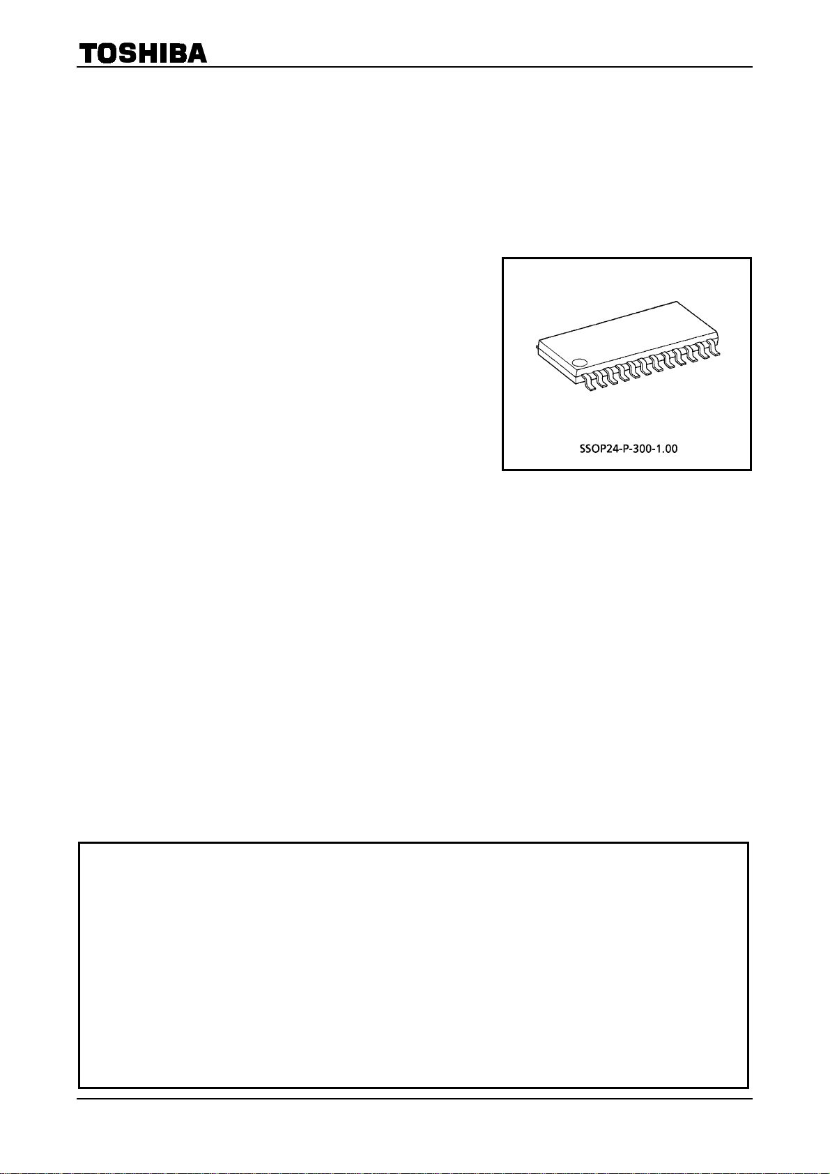
PACKAGE DIEMENSIONS
TA8805F,TA1207F
Weight: 0.32 g (Typ.)
2001-02-26 17/17
 Loading...