

Page 1

Main features
Symbol Value Unit
T1635H Series
Snubberless™ high temperature 16 A Triacs
I
T(RMS)
V
DRM/VRRM
I
GT (Q1)
16 A
600 V
35 mA
Description
Specifically designed to operate at 150° C, the
new 16 A T1635H Triacs provide an enhanced
performance in terms of power loss and thermal
dissipation. This facilitates the optimization of
heatsink dimensioning, leading to improved space
and cost effectiveness when compared to electromechanical solutions.
Based on ST Snubberless™ technology, the
T1635H series offers high commutation switching
capabilities and high noise immunity levels on the
full range of T
The T1635H series facilitates the optimization of
the control of universal motors and inductive
loads found in appliances such as vacuum
cleaners, and washing machines.
The T1635H Triacs are also suitable for use in
high temperature environment found in hot
appliances such as cookers, ovens, hobs, electric
heaters, and coffee machines.
.
j
A2
G
A2
A1
2
PAK
D
T1635H-G
A2
TO-220AB Insulated
T1635H-I
G
A2
A1
TO-220AB
T1635H-T
Order code
Part number Marking
T1635H-600G T1635H-600G
T1635H-600G-TR T1635H-600G
T1635H-600TRG T1635H-600T
T1635H-600IRG T1635H-600I
A1
A1
A2
A2
G
G
TM: Snubberless is a trademark of STMicroelectronics
August 2006 Rev 1 1/10
www.st.com
Page 2

Characteristics T1635H Series
1 Characteristics
Table 1. Absolute maximum ratings
Symbol Parameter Value Unit
2
D
I
T(RMS)
I
TSM
RMS on-state current (full sine wave)
Non repetitive surge peak on-state current
(full cycle sine wave, Tj initial = 25° C)
PA K
TO-220AB
TO-220AB Ins T
F = 60 Hz t = 16.7 ms 170
F = 50 Hz t = 20 ms 160
= 130° C
T
c
= 110° C
c
16 A
I²t I²t Value for fusing tp = 10 ms 128 A
dI/dt
V
DSM/VRSM
I
GM
P
G(AV)
T
stg
T
j
Table 2. Electrical characteristics (Tj = 25° C, unless otherwise specified)
Critical rate of rise of on-state current
I
= 2xIGT, tr ≤ 100 ns
G
F = 120 Hz T
= 150° C 50 A/µs
j
Non repetitive surge peak off state voltage Tj = 25° C 700 V
Peak gate current tp = 20 µs Tj = 150° C 4 A
Average gate power dissipation Tj = 150° C 1 W
Storage junction temperature range
Operating junction temperature range
-40 to +150
-40 to +150
Symbol Test conditions Quadrant Value Unit
(1)
I
GT
V
V
IH
GT
GD
(2)
VD = 12 V, RL = 33 Ω
VD = V
, RL =3.3 kΩ II - III MIN 0.15
DRM
IT = 100 mA MAX 35
II - III MAX 35
II - III MAX 1.3
mA
V
V
mA
A
° C
2
s
I
L
dV/dt
(dI/dt)c
1. minimum IGT is guaranteed at 5% of IGT max
2. for both polarities of A2 referenced to A1
IG = 1.2 x I
(2)
VD = 67% V
(2)
Without snubber, Tj = 150° C MIN 7.1
GT
gate open, Tj = 150° C MIN 300
DRM,
2/10
I - III
MAX
II 80
50
mA
V/µs
A/ms
Page 3

T1635H Series Characteristics
Table 3. Static electrical characteristics
Symbol Test conditions Value Unit
(1)
V
V
TM
TO
R
I
DRM
I
RRM
(1)
(1)
D
ITM= 22.5 A, tp = 380 µs Tj = 25° C MAX 1.5 V
Tj = 150° C MAX 0.80 V
Tj = 150° C MAX 23 mΩ
V
Tj = 25° C
= V
V
DRM
D/VR
RRM
Tj = 150° C 6.4
MAX
= 400 V (at peak mains voltage) Tj = 150° C 4.2
5µA
1. for both polarities of A2 referenced to A1
Table 4. Thermal resistance
Symbol Parameter Value Unit
2
PA K
R
th (j-c)
Junction to case (AC)
D
TO-220AB
1.2
TO-220AB Ins 2.1
= 1 cm² D2PA K 4 5
S
CU
R
th (j-a)
Junction to ambient
TO-220AB
TO-220AB Ins
60
mA
°C/W
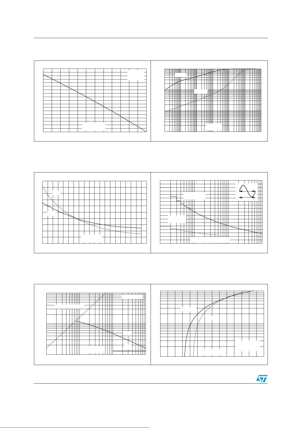
Figure 1. Maximum power dissipation
vs RMS on-state current (full cycle)
P(W)
18
α=180 °
16
14
12
10
8
6
4
2
0
0246810121416
I
T(RMS)
(A)
180°
Figure 2. RMS on-state current vs case
temperature (full cycle)
I
(A)
T(RMS)
18
16
14
12
10
8
6
4
2
α=180 °
0
0 25 50 75 100 125 150
TC(°C)
TO-220AB
Insulated
TO-220AB/D²PAK
3/10
Page 4
Characteristics T1635H Series
Figure 3. RMS on-state current vs ambient
temperature, PCB FR4, e
I
(A)
T(RMS)
4.5
4.0
3.5
3.0
2.5
2.0
1.5
1.0
0.5
0.0
0 25 50 75 100 125 150
T
(°C)
amb
= 35 µm
CU
α=180 °
D²PAK
S
CU
=1 cm²
Figure 5. Relative variation of gate trigger
current, holding current and
latching current vs junction
temperature (typical values)
IGT,IH,IL[Tj]/IGT,IH,IL[Tj=25°C]
2.5
2.0
1.5
1.0
0.5
0.0
I
GT
IH& I
L
Tj(°C)
-40 -20 0 20 40 60 80 100 120 140 160
Figure 4. Relative variation of thermal
impedance vs pulse duration
K=[Zth/Rth]
1.E+00
Z
th(j-c)
1.E-01
1.E-02
1.E-03
1.E-03 1.E-02 1.E-01 1.E+00 1.E+01 1.E+02 1.E+03
Z
th(j-a)
tP(s)
Figure 6. Surge peak on-state current vs
number of cycles
I
(A)
TSM
180
160
140
120
Non repetitive
T
initial=25 °C
j
100
80
60
Repetitive
T
=113 °C
c
40
20
0
Number of cycles
1 10 100 1000
t=20ms
One cycle
Figure 7. Non repetitive surge peak
on-state current (sinusoidal pulse
width tp<10 ms) and corresponding
value of I²t
I
(A), I²t (A²s)
TSM
10000
dI/dt limitation: 50 A/µs
1000
tP(ms)
100
0.01 0.10 1.00 10.00
4/10
Tj initial=25 °C
I
TSM
I²t
Figure 8. On-state characteristics (maximum
values)
ITM(A)
100
Tj=150 °C
Tj=25 °C
10
Tjmax. :
V
= 0.80 V
T0
R
= 23 mW
1
0.0 0.5 1.0 1.5 2.0 2.5 3.0 3.5
VTM(V)
D
Page 5
T1635H Series Characteristics
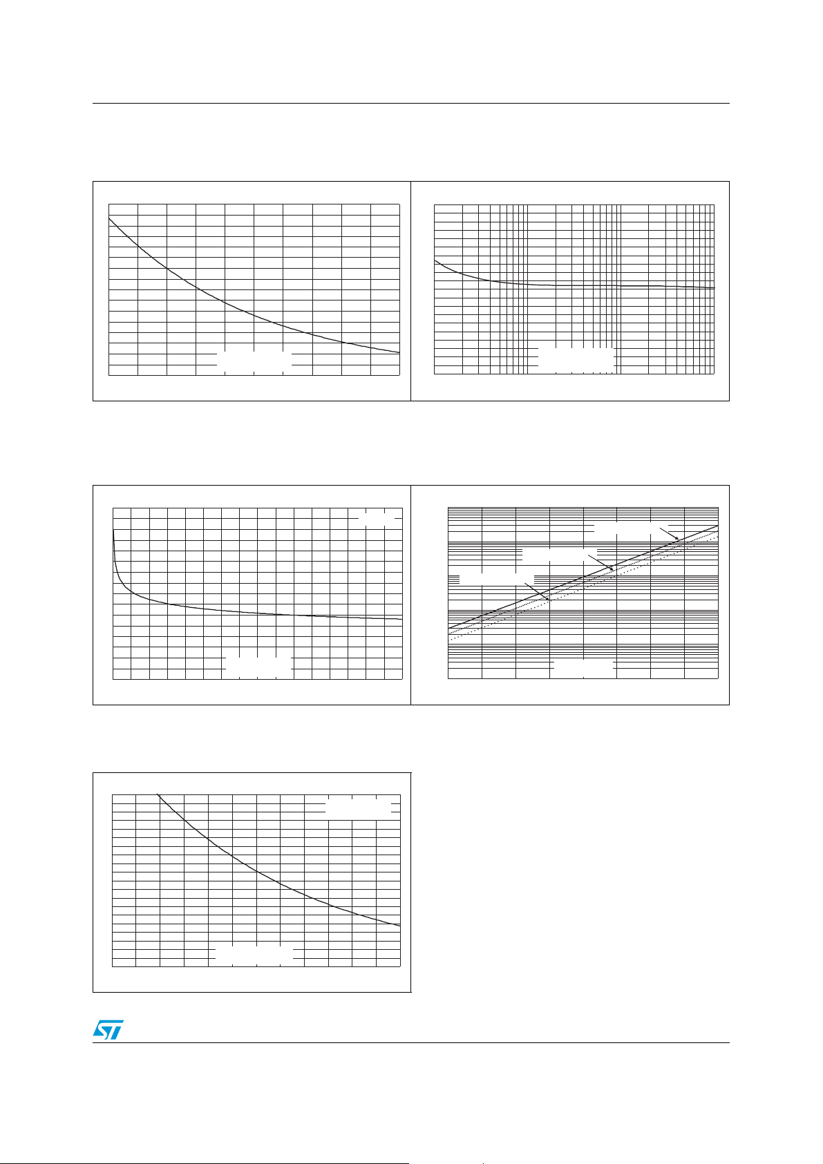
Figure 9. Relative variation of critical rate
of decrease of main current (di/dt)c
versus junction temperature
(dI/dt)c[Tj]/(dI/dt)c[Tj=150°C]
8
7
6
5
4
3
2
1
0
25 50 75 100 125 150
Tj(°C)
Figure 11. Variation of thermal resistance,
junction to ambient versus copper
surface under tab (PCB FR4,
e
35 µm)
CU
R
(°C/W)
th(j-a)
80
70
60
50
40
30
20
10
0
0 5 10 15 20 25 30 35 40
SCU(cm²)
D²PAK
Figure 10. Relative variation of critical rate of
decrease of main current (di/dt)c vs
reapplied dV/dt (typical values)
(dI/dt)c[(dV/dt)c] / Specified (dI/dt)
2.0
1.8
1.6
1.4
1.2
1.0
0.8
0.6
0.4
0.2
0.0
0.1 1.0 10.0 100.0
c
dV/dt (V/µs)
Figure 12. Leakage current versus junction
temperature for different values of
blocking voltage (typical values)
I
(mA)
DRM/IRRM
1.E+01
V
=600 VV
=600 V
DRM=VRRM
1.E+00
1.E-01
1.E-02
1.E-03
1.E-04
V
DRM=VRRM
DRM=VRRM
50 75 100 125 150
=200 VV
=200 V
V
DRM=VRRM
DRM=VRRM
=400 VV
=400 V
DRM=VRRM
Tj(°C)
Figure 13. Acceptable repetitive peak
off-state voltage versus caseambient thermal resistance
R
(°C/W)
th(c-a)
10
9
8
7
6
5
4
3
2
1
0
300 350 400 450 500 550 600
V
DRM/VRRM
(V)
R
th(j-c)
T
J
=1.2 °C/W
=150 °C
5/10
Page 6

Ordering information scheme T1635H Series
2 Ordering information scheme
T 16 35 H - 600 I (-TR)
Triac series
Current
16 = 16 A
Sensitivity
35 = 35 mA
High temperature
Voltage
600 = 600 V
Package
2
G = D PAK
I = TO-220AB Ins
T = TO-220AB
Packing mode
Blank = Tube (D PAK)
-TR = Tape and reel (
2
D PAK)
RG = Tube (TO-220AB)
2
6/10
Page 7
T1635H Series Package information
3 Package information
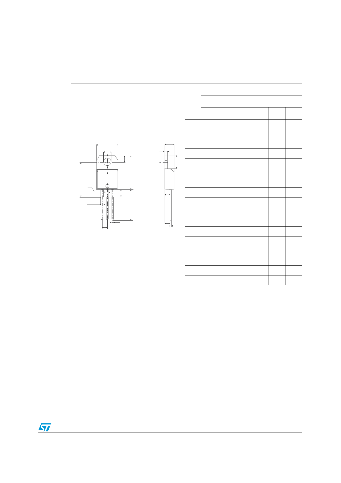
Table 5. TO-220AB and TO-220AB Insulated dimensions
Dimensions
Ref.
Millimeters Inches
Min. Typ. Max. Min. Typ. Max.
A 15.20 15.90 0.598 0.625
a1 3.75 0.147
B
Ø I
L
A
I4
l3
a1
l2
a2
C
b2
a2 13.00 14.00 0.511 0.551
B 10.00 10.40 0.393 0.409
F
b1 0.61 0.88 0.024 0.034
b2 1.23 1.32 0.048 0.051
C 4.40 4.60 0.173 0.181
c2
c1 0.49 0.70 0.019 0.027
c2 2.40 2.72 0.094 0.107
e 2.40 2.70 0.094 0.106
M
b1
e
c1
F 6.20 6.60 0.244 0.259
ØI 3.75 3.85 0.147 0.151
I4 15.80 16.40 16.80 0.622 0.646 0.661
L 2.65 2.95 0.104 0.116
l2 1.14 1.70 0.044 0.066
l3 1.14 1.70 0.044 0.066
M 2.60 0.102
7/10
Page 8
Package information T1635H Series
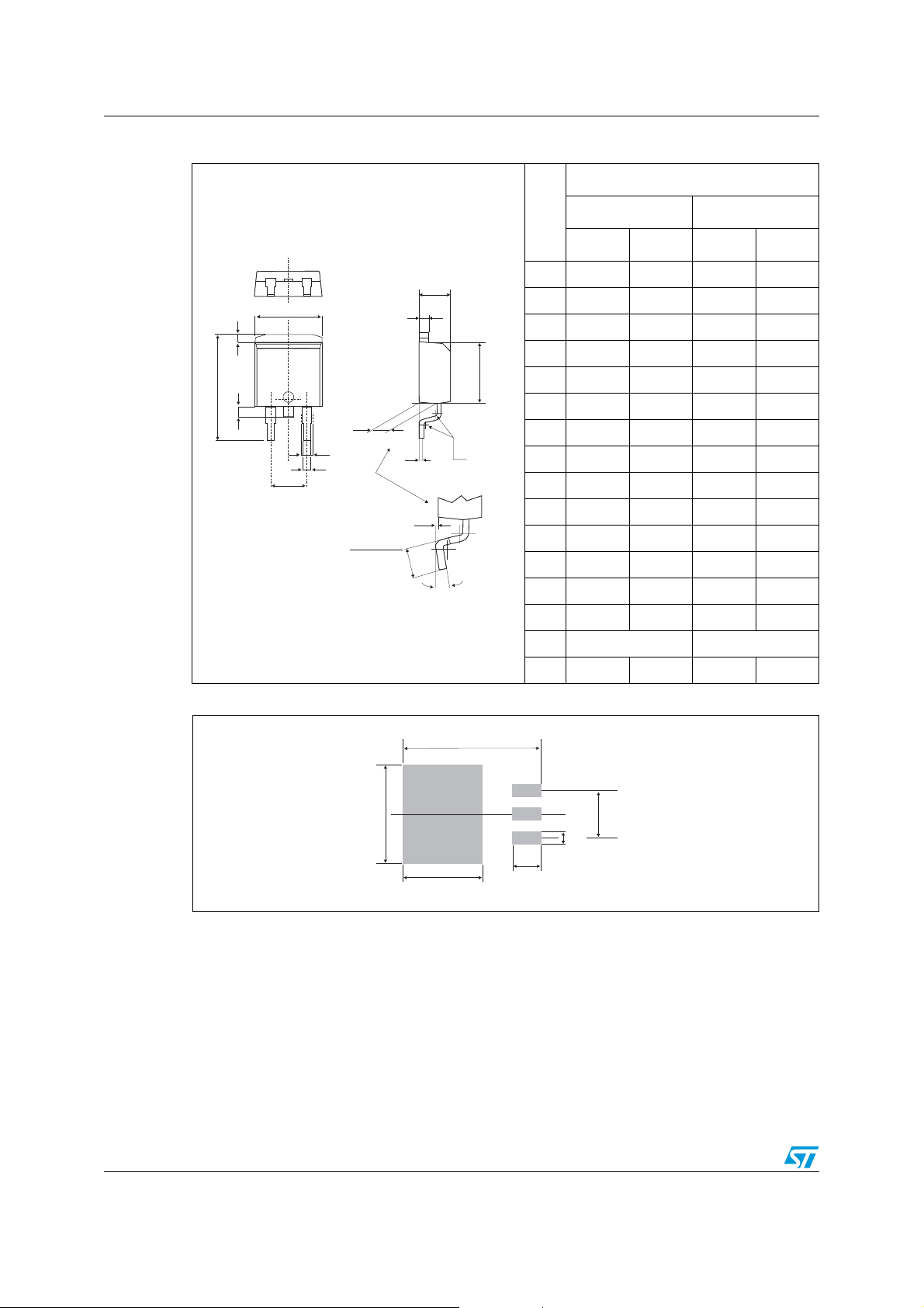
Table 6. D
L2
L
L3
2
PAK Mechanical data
E
B2
B
G
A1
2mm min.
FLAT ZONE
C2
C
DIMENSIONS
REF.
Millimeters Inches
Min. Max. Min. Max.
A 4.40 4.60 0.173 0.181
A
A1 2.49 2.69 0.098 0.106
A2 0.03 0.23 0.001 0.009
B 0.70 0.93 0.027 0.037
D
B2 1.14 1.70 0.045 0.067
C 0.45 0.60 0.017 0.024
C2 1.23 1.36 0.048 0.054
R
D 8.95 9.35 0.352 0.368
E 10.00 10.40 0.393 0.409
A2
G 4.88 5.28 0.192 0.208
L 15.00 15.85 0.590 0.624
V2
L2 1.27 1.40 0.050 0.055
L3 1.40 1.75 0.055 0.069
M 2.40 3.20 0.094 0.126
R 0.40 typ. 0.016 typ.
V2 0° 8° 0° 8°
Figure 14. D2PAK Footprint (dimensions in mm)
16.90
10.30
8.90
3.70
5.08
1.30
In order to meet environmental requirements, ST offers these devices in ECOPACK®
packages. These packages have a Lead-free second level interconnect . The category of
second level interconnect is marked on the package and on the inner box label, in
compliance with JEDEC Standard JESD97. The maximum ratings related to soldering
conditions are also marked on the inner box label. ECOPACK is an ST trademark.
ECOPACK specifications are available at: www.st.com.
8/10
Page 9
T1635H Series Ordering information
4 Ordering information
Part number Marking Package Weight Base Qty Packing mode
T1635H-600G T1635H-600G D
T1635H-600G-TR T1635H-600G D
2
PAK 1.5 g 50 Tube
2
PAK 1.5 g 1000 Tape and Reel
T1635H-600TRG T1635H-600T TO-220AB 2.3 g 50 Tube
T1635H-600IRG T1635H-600I TO-220AB Ins 2.3 g 50 Tube
5 Revision history
Date Revision Changes
31-Aug-2006 1 Initial release
9/10
Page 10

T1635H Series
Please Read Carefully:
Information in this document is provided solely in connection with ST products. STMicroelectronics NV and its subsidiaries (“ST”) reserve the
right to make changes, corrections, modifications or improvements, to this document, and the products and services described herein at any
time, without notice.
All ST products are sold pursuant to ST’s terms and conditions of sale.
Purchasers are solely responsible for the choice, selection and use of the ST products and services described herein, and ST assumes no
liability whatsoever relating to the choice, selection or use of the ST products and services described herein.
No license, express or implied, by estoppel or otherwise, to any intellectual property rights is granted under this document. If any part of this
document refers to any third party products or services it shall not be deemed a license grant by ST for the use of such third party products
or services, or any intellectual property contained therein or considered as a warranty covering the use in any manner whatsoever of such
third party products or services or any intellectual property contained therein.
UNLESS OTHERWISE SET FORTH IN ST’S TERMS AND CONDITIONS OF SALE ST DISCLAIMS ANY EXPRESS OR IMPLIED
WARRANTY WITH RESPECT TO THE USE AND/OR SALE OF ST PRODUCTS INCLUDING WITHOUT LIMITATION IMPLIED
WARRANTIES OF MERCHANTABILITY, FITNESS FOR A PARTICULAR PURPOSE (AND THEIR EQUIVALENTS UNDER THE LAWS
OF ANY JURISDICTION), OR INFRINGEMENT OF ANY PATENT, COPYRIGHT OR OTHER INTELLECTUAL PROPERTY RIGHT.
UNLESS EXPRESSLY APPROVED IN WRITING BY AN AUTHORIZED ST REPRESENTATIVE, ST PRODUCTS ARE NOT
RECOMMENDED, AUTHORIZED OR WARRANTED FOR USE IN MILITARY, AIR CRAFT, SPACE, LIFE SAVING, OR LIFE SUSTAINING
APPLICATIONS, NOR IN PRODUCTS OR SYSTEMS WHERE FAILURE OR MALFUNCTION MAY RESULT IN PERSONAL INJURY,
DEATH, OR SEVERE PROPERTY OR ENVIRONMENTAL DAMAGE. ST PRODUCTS WHICH ARE NOT SPECIFIED AS "AUTOMOTIVE
GRADE" MAY ONLY BE USED IN AUTOMOTIVE APPLICATIONS AT USER’S OWN RISK.
Resale of ST products with provisions different from the statements and/or technical features set forth in this document shall immediately void
any warranty granted by ST for the ST product or service described herein and shall not create or extend in any manner whatsoever, any
liability of ST.
ST and the ST logo are trademarks or registered trademarks of ST in various countries.
Information in this document supersedes and replaces all information previously supplied.
The ST logo is a registered trademark of STMicroelectronics. All other names are the property of their respective owners.
© 2006 STMicroelectronics - All rights reserved
STMicroelectronics group of companies
Australia - Belgium - Brazil - Canada - China - Czech Republic - Finland - France - Germany - Hong Kong - India - Israel - Italy - Japan -
Malaysia - Malta - Morocco - Singapore - Spain - Sweden - Switzerland - United Kingdom - United States of America
www.st.com
10/10
 Loading...