

Page 1
Micrel, Inc.
3.3V, 1.5GHz ÷1/÷2 DIFFERENTIAL
LVECL/LVPECL PROGRAMMABLE CLOCK
GENERATOR AND 1:15 FANOUT BUFFER
FEATURES
■ Four programmable output banks and 15 total
LVPECL-compatible differential outputs
■ Pin-compatible, plug-in replacement to
MC100LVE222FA
■ f
clock = 1.5GHz
MAX
■ 50ps output-to-output skew
■ Four output banks with independent ÷1, ÷2
frequency control
■ 100k compatible I/O
■ Power supply 3.3V ±10%
■ –40°C to +85°C temperature range
■ Available in 52-pin LQFP package
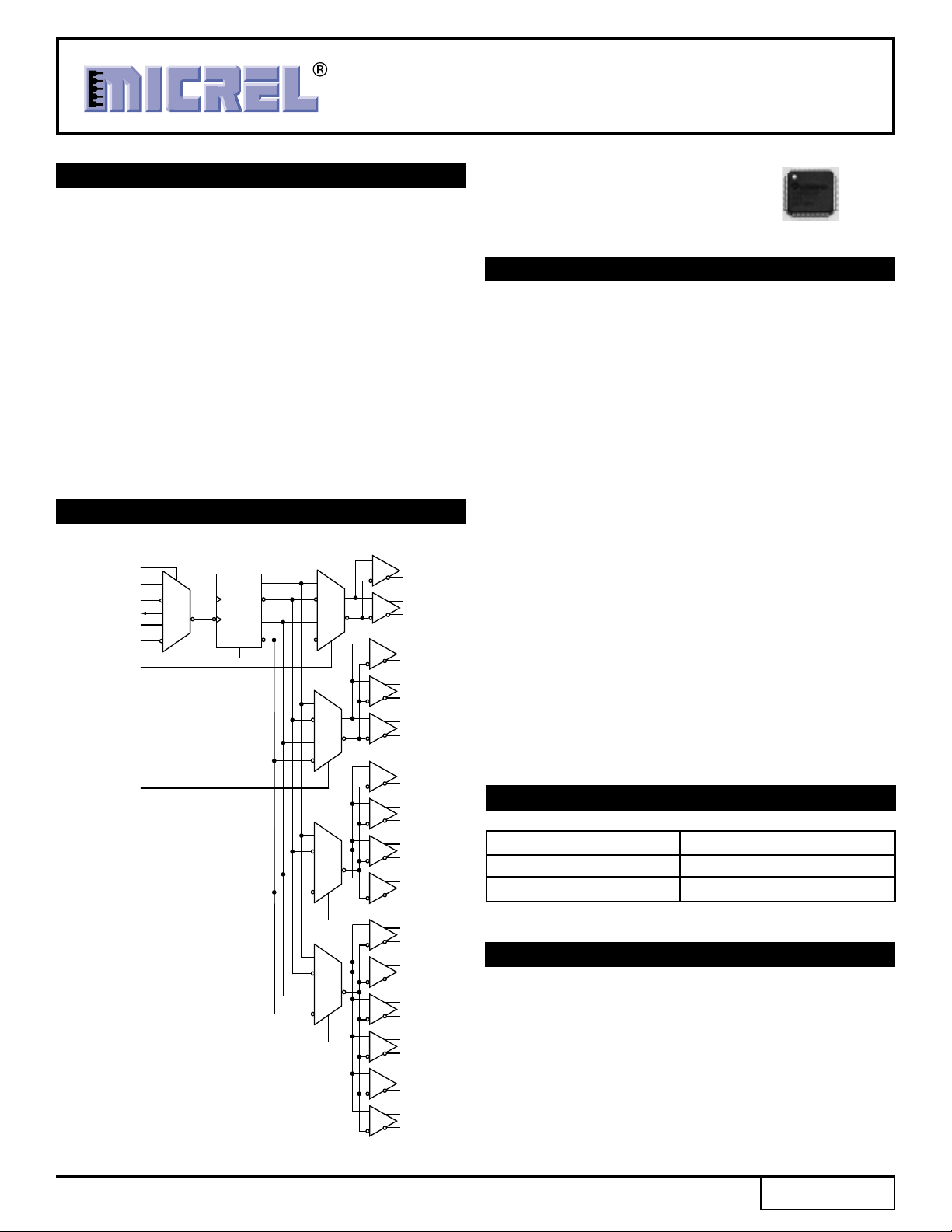
FUNCTIONAL BLOCK DIAGRAM
1:2 FOB
CLK_SEL
CLK0
/CLK0
V
CLK1
/CLK1
MR
FSELA
FSELB
FSELC
FSELD
2:1
BB
MUX
CLK
÷1
÷2
2:1
MUX
2:1
MUX
2:1
MUX
2:1
MUX
1:3 FOB
1:4 FOB
1:6 FOB
QA0
/QA0
QA1
/QA1
QB0
/QB0
QB1
/QB1
QB2
/QB2
QC0
/QC0
QC1
/QC1
QC2
/QC2
QC3
/QC3
QD0
/QD0
QD1
/QD1
QD2
/QD2
QD3
/QD3
QD4
/QD4
QD5
/QD5
Precision Edge
Precision Edge
SY100E222L
®
SY100E222L
Precision Edge
®
DESCRIPTION
The SY100E222L is a low-skew, low-jitter device capable
of receiving a high-speed LVECL/LVPECL input in either a
single-ended or differential configuration. For single-ended
configurations, a VBB output reference is supplied by the
SY100E222L. A 2:1 input multiplexer selects from two
differential input pairs by means of the CLK_SEL input select.
The internal programmable divider for each of the four
banks generates a ÷1 or ÷2 frequency of the selected input.
The ÷1/÷2 divider outputs can be asynchronously
synchronized with the master reset (MR) input so that the
outputs will start out in a known state.
The 15 total outputs are partitioned into four independently
selected output banks in a 2/3/4/6 fanout configuration. Each
of the four banks can independently select the ÷1 or ÷2
output frequency by means of the four separate frequency
select pins (FSELA-FSELD) inputs.
The SY100E222L is pin-for-pin compatible with the
MC100LVE222FA device.
The SY100E222L is part of a Micrel’s Precision Edge
product family. For other integrated clock divider plus fanout
buffer options, consider Micrel’s SY89200 family.
All support documentation can be found on Micrel’s web
site at: www.micrel.com.
CROSS REFERENCE TABLE
Micrel Part Number ON Semiconductor
SY100E222LTI MC100LVE222FA
SY100E222LTI TR MC100LVE222FAR2
APPLICATIONS
■ SONET/SDH channel applications
■ Fibre Channel multi-channel applications
■ Gigabit Ethernet multi-channel applications
®
®
Precision Edge is a registered trademark of Micrel, Inc.
M9999-111605
hbwhelp@micrel.com or (408) 955-1690
1
Rev.: B Amendment: /0
Issue Date: November 2005
Page 2
Micrel, Inc.
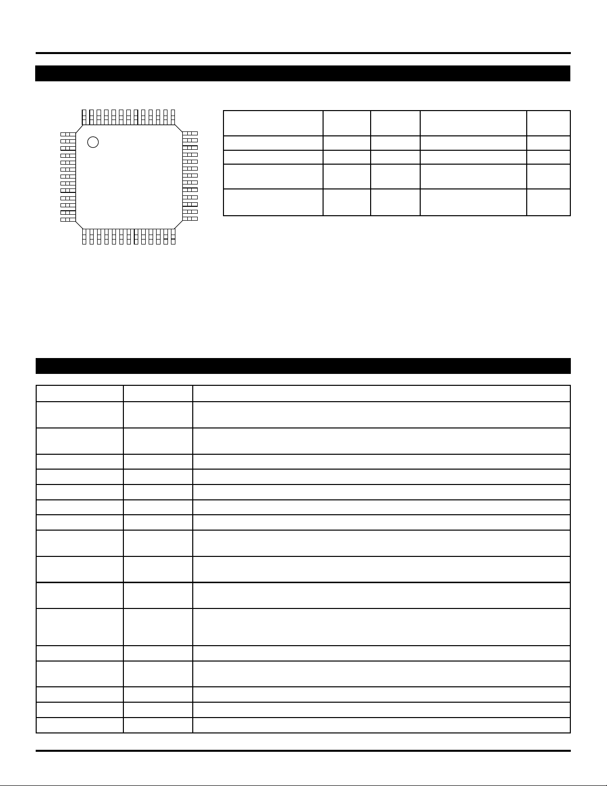
PACKAGE/ORDERING INFORMATION
Precision Edge
SY100E222L
®
VCCO
QA0
/QA0
QA1
/QA1
VCC
FSELA
FSELB
CLK0
/CLK0
CLK_SEL
CLK1
/CLK1
VBB
FSELC
FSELD
VEE
MR
52 51 50 49 48 47 46 45 44 43 42 41 40
1
2
3
4
5
6
7
8
9
10
11
12
13
14 15 16 17 18 19 20 21 22 23 24 25 26
QD5
QD4
/QD5
/QD4
VCCO
52-Pin LQFP (LQFP-52)
PIN DESCRIPTION
VCCO
/QD3
QB0
QD3
/QB0
/QD2
QB1
QD2
/QB1
/QD1
QB2
QD1
/QB2
/QD0
VCCO
39
38
37
36
35
34
33
32
31
30
29
28
27
QD0
Ordering Information
(1)
Package Operating Package Lead
Part Number Type Range Marking Finish
VCCO
QC0
SY100E222LTI LQFP-52 Industrial SY100E222L Sn-Pb
/QC0
QC1
SY100E222LTITR
/QC1
QC2
SY100E222LTY
/QC2
QC3
/QC3
VCCO
SY100E222LTYTR
NC
NC
VCCO
Notes:
1. Contact factory for die availability. Dice are guaranteed at TA = 25°C, DC Electricals only.
2. Tape and Reel.
3. Pb-Free package is recommended for new designs.
(3)
(2)
LQFP-52 Industrial SY100E222L Sn-Pb
LQFP-52 Industrial SY100E222L with Matte-Sn
Pb-Free bar-line indicator Pb-Free
(2, 3)
LQFP-52 Industrial SY100E222L with Matte-Sn
Pb-Free bar-line indicator Pb-Free
Pin Number Pin Name Pin Function
2 MR 100k ECL compatible: Master reset function resets all outputs to a differential LOW when
MR pin goes HIGH.
5, 6, CLK0, /CLK0, Differential inputs: These input pairs are the differential signal inputs to the device. Inputs
8, 9 CLK1, /CLK1 accept 100k LVPECL/LVECL levels.
7 CLK_SEL 100k ECL compatible input select. LOW = CLK0, HIGH= CLK1.
3 FSELA 100k ECL compatible bank A output select. LOW: QA0-QA1 = ÷1, HIGH: QA0-QA1 = ÷2.
4 FSELB 100k ECL compatible bank B output select. LOW: QB0-QB2 = ÷1, HIGH: QB0-QB2 = ÷2.
11 FSELC 100k ECL compatible bank C output select. LOW: QC0-QC3 = ÷1, HIGH: QC0-QC3 = ÷2.
12 FSELD 100k ECL compatible bank D output select. LOW: QD0-QD5 = ÷1, HIGH: QD0-QD5 = ÷2.
51, 49, QA0 – QA1, Bank A 100k differential output pairs controlled by FSELA.
50, 48 /QA0 – /QA1 FSELA: LOW, QA = ÷1, HIGH, QA = ÷2.
46, 44, 42, QB0 – QB2, Bank B 100k differential output pairs controlled by FSELB.
45, 43, 41 /QB0 – /QB2 FSELB: LOW, QB = ÷1, HIGH, QB = ÷2.
38, 36, 34, 32, QC0 – QC3, Bank C 100k differential output pairs controlled by FSELC.
37, 35, 33, 31 /QC0 – /QC3 FSELC: LOW, QC = ÷1, HIGH, QC = ÷2.
26, 24, 22, 20, QD0 – QD5, Bank D 100k differential output pairs controlled by FSELD.
18, 16, 25, 23, /QD0 – /QD5 FSELD: LOW, QD = ÷1, HIGH, QD = ÷2.
21, 19, 17, 15
1 VCC Positive power supply: Bypass with 0.1µF0.01µF low ESR capacitors.
14, 27, 30, 39, VCCO Positive power supply for output buffers. Bypass with 0.1µF0.01µF low ESR capacitors.
40, 47, 52
13 VEE Negative power supply. For LVPECL systems, VEE is GND.
10 VBB Reference voltage.
28, 29 NC No connect: Not internally connected (unused pins).
M9999-111605
hbwhelp@micrel.com or (408) 955-1690
2
Page 3

Micrel, Inc.
Precision Edge
SY100E222L
®
Absolute Maximum Ratings
(1)
Supply Voltage (VCC) ................................. –0.5V to + 4.0V
Input Voltage (V
Termination Current
) ......................................... –0.5V to V
IN
(3)
CC
Source or sink current on VBB (IBB).....................±0.5mA
DC Output Current
LVPECL Outputs..................................................–50mA
Operating Ratings
Supply Voltage (VCC) ..................................+3.0V to +3.6V
Ambient Temperature (TA)......................... –40°C to +85°C
Package Thermal Resistance
LQFP (θJA)
Still-Air................................................................ 70°C/W
500lfpm .............................................................. 48°C/W
(2)
Lead Temperature (soldering, 20 sec.) ...................+260°C
Storage Temperature (T
DC ELECTRICAL CHARACTERISTICS
Symbol Parameter Condition Min Typ Max Units
I
CC
Power Supply Current Max. VCC all inputs and outputs OPEN 122 139 mA
LVPECL DC ELECTRICAL CHARACTERISTICS
VCC = +3.3V ±0.3V; VEE = 0V; TA = –40°C to +85°C, typicals are TA = 25°C.
Symbol Parameter Condition Min Typ Max Units
V
OH
V
OL
V
IH
V
IL
V
IHCMR
V
BB
I
IH
I
IL
Output High Voltage RL = 50Ω to VCC–2V 2215 2345 2420 mV
Output Low Voltage RL = 50Ω to VCC–2V 1470 1595 1680 mV
Input High Voltage 2135 2420 mV
Input Low Voltage 1490 1825 mV
Input High Voltage Common Note 6
Mode Range (Differential)
Output Reference Voltage 1.92 2.04 V
Input HIGH Current 150 µA
Input LOW Current
) ...................... –65°C to +150°C
S
(4)
(4, 5)
(CLK, /CLK) V
< 500mV 1.3 2.9 V
PP
VPP ≥ 500mV 1.6 2.9 V
(CLK, CLK_SEL, FSEL, MR) 0.5 µA
(/CLK) –300 µA
Notes:
1. Permanent device damage may occur if the ratings in “Absolute Maximum Ratings” section are exceeded. This is a stress rating only and functional
operation is not implied at conditions other than those detailed in the operational sections of this data sheet. Exposure to absolute maximum ratings
conditions for extended periods may affect device reliability.
2. The data sheet limits are not guaranteed if the device is operated beyond the operating ratings.
3. Due to the limited drive capability use for input of the same package only.
4. The circuit is designed to meet the DC specifications shown in the above table after thermal equilibrium has been established.
5. Input and output parameters are for VCC = 3.3V. They vary 1:1 with VCC.
6. V
M9999-111605
hbwhelp@micrel.com or (408) 955-1690
is defined as the range within which the VIH level may vary with the device still meeting the propagation delay specification. The VIL level
IHCMR
must be such that the peak-to-peak voltage is less than 1.0V and then greater than or equal to VPP(min).
3
Page 4

Micrel, Inc.
Precision Edge
SY100E222L
®
LVECL DC ELECTRICAL CHARACTERISTICS
(5)
VCC = 0V; VEE = –3.3V ±0.3V; TA = –40°C to +85°C, typicals are TA = 25°C.
Symbol Parameter Condition Min Typ Max Units
V
OH
V
OL
V
IH
V
IL
V
IIHCMR
Output High Voltage RL = 50Ω to VCC–2V –1085 –955 –880 mV
Output Low Voltage RL = 50Ω to VCC–2V –1830 –1705 –1620 mV
Input High Voltage –1165 –880 mV
Input Low Voltage –1810 –1475 mV
Input High Voltage Common Note 6
Mode Range (Differential)
(CLK, /CLK) V
< 500mV –2.0 –0.4 V
PP
VPP ≥ 500mV –1.7 –0.4 V
V
BB
I
IH
I
IL
Output Reference Voltage –1.38 –1.26 V
Input HIGH Current 150 µA
Input LOW Current
(CLK, CLK_SEL, FSEL, MR) 0.5 µA
(/CLK) –300 µA
AC ELECTRICAL CHARACTERISTICS
(7)
VCC = +3.0 to +3.6V and VEE = 0V or VCC = 0V and VEE = –3.0 to –3.6V; TA = –40°C to +85°C, typicals are TA = 25°C.
Symbol Parameter Condition Min Typ Max Units
f
MAX
t
pd
Maximum Operating Frequency 1.2 >1.5 GHz
Propagation Delay IN (Differential), Note 8 1040 1210 1420 ps
IN (Single-ended), Note 9 1090 1335 1570 ps
MR 1000 1200 1520 ps
t
SKEW
Within-Device Skew Note 10 50 ps
Part-to-Part Skew (Differential) 300 ps
t
JITTER
V
PP
tr, t
f
Notes:
5. The circuit is designed to meet the DC specifications shown in the above table after thermal equilibrium has been established.
6. V
IHCMR
must be such that the peak-to-peak voltage is less than 1.0V and then greater than or equal to VPP(min).
7. High-frequency AC parameters are guaranteed by design and characterization.
8. The differential propagation delay is defined as the delay from the crossing points of the differential input signals to the crossing point of the
differential output signals.
9. The single-ended propagation delay is defined as the delay from the 50% point of the input signal to the 50% point of the output signal.
10. The within-device skew is defined as the worst-case difference between any two similar delay paths within a single device.
11. VPP(min) is defined as the minimum input differential voltage, which will cause no increase in the propagation delay. The VPP(min) is AC limited for
the SY100E222L as a differential input as low as 50 mV will still produce full ECL levels at the output.
Random Clock Jitter < 1 ps
Differential Input Swing Note 11 400 1000 mV
Output Rise/Fall Time (Q, /Q) (20% to 80%) 200 600 ps
is defined as the range within which the VIH level may vary with the device still meeting the propagation delay specification. The VIL level
RMS
M9999-111605
hbwhelp@micrel.com or (408) 955-1690
4
Page 5

Micrel, Inc.
SINGLE-ENDED AND DIFFERENTIAL SWINGS
VIN,
350mV (Typ.)
V
OUT
V
DIFF_IN
V
DIFF_OUT
Precision Edge
SY100E222L
,
700mV (Typ.)
®
Figure 1a. Single-Ended Voltage Swing
TIMING DIAGRAM
CLK
/CLK
MR
Q
÷1
/Q
Q
÷2
/Q
Figure 1b. Differential Voltage Swing
TRUTH TABLE
M9999-111605
hbwhelp@micrel.com or (408) 955-1690
MR
CLK_SEL
FSEL Q
0 0 0 CLK0 ÷ 1
0 0 1 CLK0 ÷ 2
0 1 0 CLK1 ÷ 1
0 1 1 CLK1 ÷ 2
1X X 0
5
Page 6

Micrel, Inc.
52-PIN LQFP (LQFP-52)
Precision Edge
SY100E222L
®
MICREL, INC. 2180 FORTUNE DRIVE SAN JOSE, CA 95131 USA
TEL + 1 (408) 944-0800 FAX + 1 (408) 474-1000 WEB http://www.micrel.com
The information furnished by Micrel in this data sheet is believed to be accurate and reliable. However, no responsibility is assumed by Micrel for its use.
Micrel Products are not designed or authorized for use as components in life support appliances, devices or systems where malfunction of a product can
reasonably be expected to result in personal injury. Life support devices or systems are devices or systems that (a) are intended for surgical implant into
the body or (b) support or sustain life, and whose failure to perform can be reasonably expected to result in a significant injury to the user. A Purchaser’s
use or sale of Micrel Products for use in life support appliances, devices or systems is at Purchaser’s own risk and Purchaser agrees to fully indemnify
M9999-111605
hbwhelp@micrel.com or (408) 955-1690
Micrel reserves the right to change circuitry and specifications at any time without notification to the customer.
Micrel for any damages resulting from such use or sale.
© 2005 Micrel, Incorporated.
6
 Loading...