

Page 1
查询SY100E137JZTR供应商
Micrel, Inc.
8-BIT RIPPLE
COUNTER
SY10E137
SY100E137
SY10E137
SY100E137
FEATURES
■ 1.8GHz min. count frequency
■ Extended 100E V
EE range of –4.2V to –5.5V
■ Synchronous and asynchronous enable pins
■ Differential clock input and data output pins
■ VBB output for single-ended use
■ Asynchronous Master Reset
■ Internal 75KΩ input pull-down resistors
■ Available in 28-pin PLCC packge
PIN NAMES
Pin Function
CLK, CLK Differential Clock Inputs
Q0–Q7, Q0–Q7 Differential Q Outputs
A_Start Asynchronous Enable Input
EN1, EN2 Synchronous Enable Inputs
MR Asynchronous Master Reset
VBB Switching Reference Output
VCCO VCC to Output
DESCRIPTION
The SY10/100E137 are very high speed binary ripple
counters. The two least significant bits were designed
with very fast edge rates, while the more significant bits
maintain standard ECLinPS output edge rates. This allows
the counters to operate at very high frequencies, while
maintaining a moderate power dissipation level.
The devices are ideally suited for multiple frequency
clock generation, as well as for counters in highperformance ATE time measurement boards.
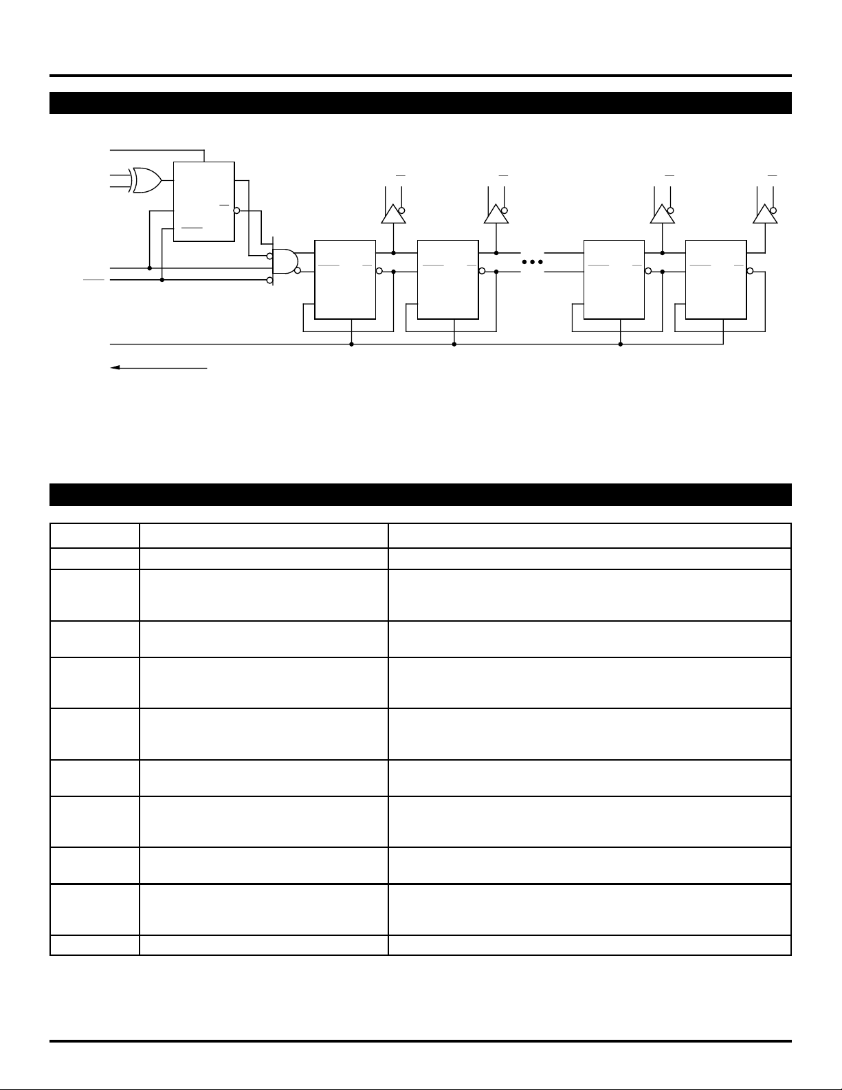
Both asynchronous and synchronous enables are
available to maximize the device's flexibility for various
applications. The asynchronous enable input, A_Start,
when asserted, enables the counter while overriding any
synchronous enable signals. The E137 features XOR'ed
enable inputs, EN
the CLK input. When only one synchronous enable is
asserted, the counter becomes disabled on the next CLK
transition. All outputs remain in the previous state poised
for the other synchronous enable or A_Start to be
asserted in order to re-enable the counter. Asserting
both synchronous enables causes the counter to become
enabled on the next transition of the CLK. EN1 (or EN2)
and CLK edges are coincident. Sufficient delay has been
inserted in the CLK path (to compensate for the XOR
gate delay and the internal D-flip-flop set-up time) to
ensure that the synchronous enable signal is clocked
correctly; hence, the counter is disabled.
The E137 can also be driven single-endedly utilizing
the VBB output supply as the voltage reference for the
CLK input signal. If a single-ended signal is to be used,
the VBB pin should be connected to the CLK input and
bypassed to ground via a 0.01µF capacitor. VBB can
only source/sink 0.5mA; therefore, it should be used as
a switching reference for the E137 only.
All input pins left open will be pulled LOW via an input
pull-down resistor. Therefore, do not leave the differential
CLK inputs open. Doing so causes the current source
transistor of the input clock gate to become saturated,
thus upsetting the internal bias regulators and
jeopardizing the stability of the device.
The asynchronous Master Reset resets the counter to
an all zero state upon assertion.
1 and EN2, which are synchronous to
M9999-032006
[email protected] or (408) 955-1690
1
Rev.: E Amendment: /0
Issue Date: March 2006
Page 2
Micrel, Inc.
K
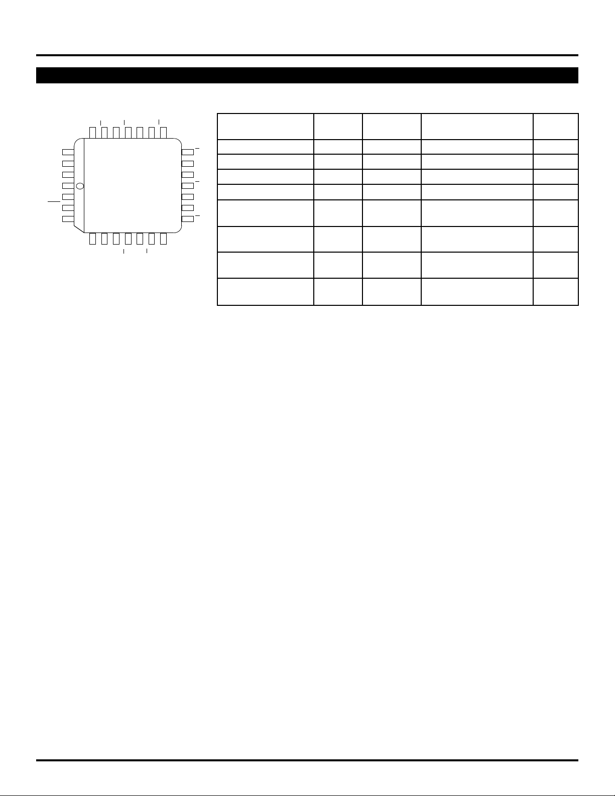
PACKAGE/ORDERING INFORMATION
SY10E137
SY100E137
A_Start
EN
EN
V
CL
CLK
V
7
7
Q
Q
25 24 23 22 21 20 19
26
1
27
2
28
EE
1
2
3
BB
4
TOP VIEW
567891011
MR
CCO
V
28-Pin PLCC (J28-1)
6
Q
PLCC
J28-1
0
Q
Ordering Information
6
Q
CCO
V
5
5
Q
Q
(1)
Package Operating Package Lead
Part Number Type Range Marking Finish
18
17
16
15
14
13
12
1
1
0
Q
Q
Q
CCO
V
SY10E137JC J28-1 Commercial SY10E137JC Sn-Pb
Q
4
SY10E137JCTR
Q
4
V
CC
SY100E137JC J28-1 Commercial SY100E137JC Sn-Pb
Q
3
SY100E137JCTR
Q
3
Q
2
SY10E137JZ
Q
2
SY10E137JZTR
(3)
(2)
(2)
(2, 3)
J28-1 Commercial SY10E137JC Sn-Pb
J28-1 Commercial SY100E137JC Sn-Pb
J28-1 Commercial SY10E137JZ with Matte-Sn
Pb-Free bar-line indicator
J28-1 Commercial SY10E137JZ with Matte-Sn
Pb-Free bar-line indicator
SY100E137JZ
(3)
J28-1 Commercial SY100E137JZ with Matte-Sn
Pb-Free bar-line indicator
SY100E137JZTR
(2, 3)
J28-1 Commercial SY100E137JZ with Matte-Sn
Pb-Free bar-line indicator
Notes:
1. Contact factory for die availability. Dice are guaranteed at TA = 25°C, DC Electricals only.
2. Tape and Reel.
3. Pb-Free package is recommended for new designs.
M9999-032006
[email protected] or (408) 955-1690
2
Page 3
Micrel, Inc.
BLOCK DIAGRAM
A_Start
EN1
EN2
CLK
CLK
MR
VBB
D
CLK
CLK
SY10E137
SY100E137
R
Q
Q
CLK
CLK
D
D
Q0Q
0
Q
Q
R
CLK
CLK
D
Q1Q
1
Q
Q
R
CLK
CLK
D
Q6Q
6
Q
Q
R
CLK
CLK
D
Q7Q
7
Q
Q
R
SEQUENTIAL TRUTH TABLE
(1)
Function EN1 EN2 A_Start MR CLK Q7 Q6 Q5 Q4 Q3 Q2 Q1 Q0
Reset X X X H X LLLLLLLL
Count LLLLZLLLLLLLH
LLLLZLLLLLLHL
LLLLZLLLLLLHH
Stop HLLLZLLLLLLHH
HLLLZLLLLLLHH
Async. Start H L H L Z LLLLLHLL
HLHLZLLLLLHLH
LLHLZLLLLLHHL
Count LLLLZLLLLLHHH
LLLLZLLLLHLLL
LLLLZLLLLHLLH
Stop LHLLZLLLLHLLH
LHLLZLLLLHLLH
Sync. Start H H L L Z LLLLHLHL
HHLLZLLLLHLHH
HHLLZLLLLHHLL
Stop HLLLZLLLLHHLL
HLLLZLLLLHHLL
Count LLLLZLLLLHHLH
LLLLZLLLLHHHL
LLLLZLLLLHHHH
Reset X X X H X LLLLLLLL
Note:
1. Z = LOW-to-HIGH transition
M9999-032006
[email protected] or (408) 955-1690
3
Page 4
Micrel, Inc.
SY100E137
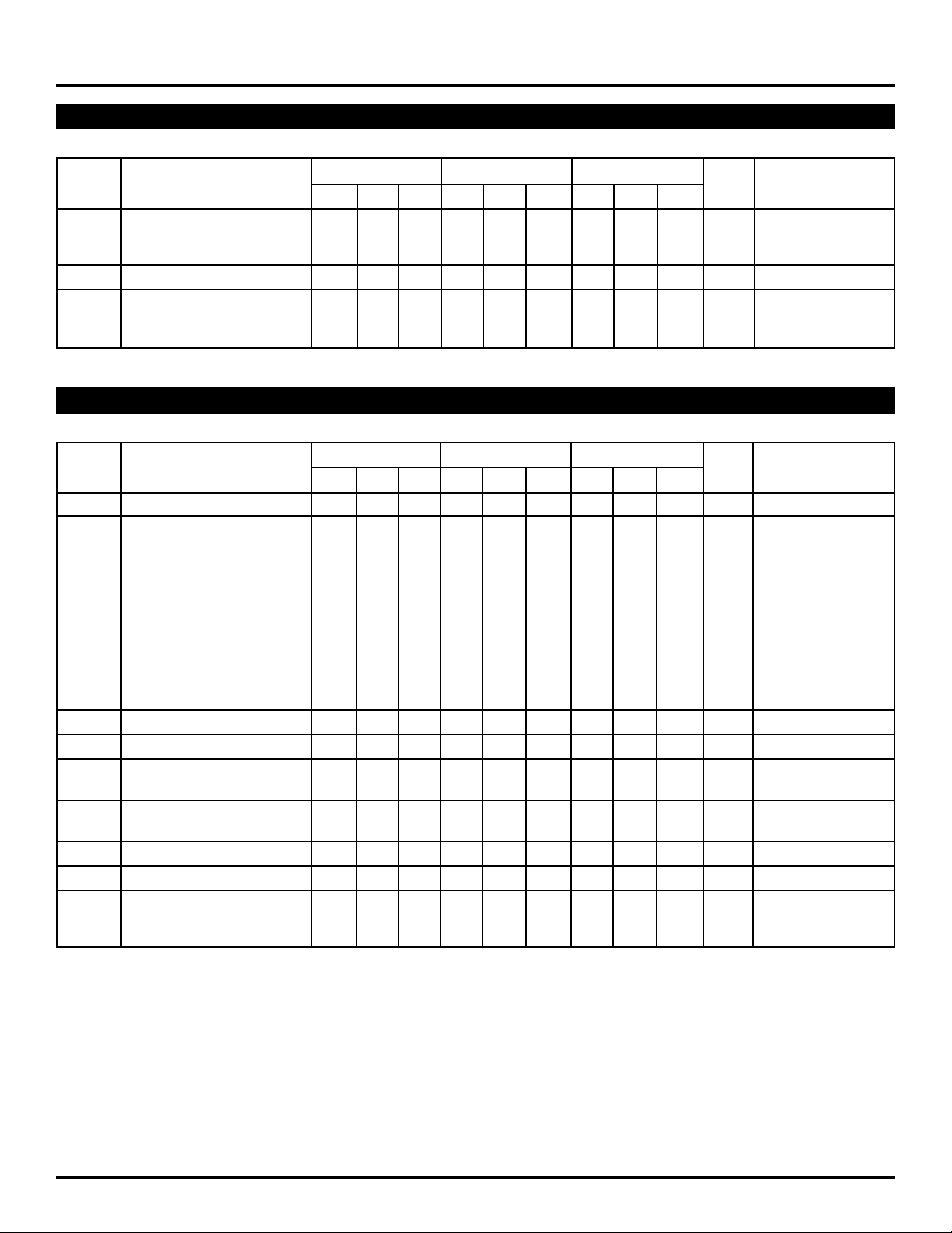
DC ELECTRICAL CHARACTERISTICS
VEE = VEE (Min.) to VEE (Max.); VCC = VCCO = GND
TA = 0°CTA = +25°CTA = +85°C
Symbol Parameter Min. Typ. Max. Min. Typ. Max. Min. Typ. Max. Unit Condition
BB Output Reference V —
V
Voltage 10E –1.38 —–1.27 –1.35 —–1.25 –1.31 —–1.19
100E –1.38 —–1.26 –1.38 —–1.26 –1.38 —–1.26
IIH Input HIGH Current ——150 ——150 ——150 µA —
I
EE Power Supply mA —
Current 10E — 121 145 — 121 145 — 121 145
100E — 121 145 — 121 145 — 139 167
AC ELECTRICAL CHARACTERISTICS
VEE = VEE (Min.) to VEE (Max.); VCC = VCCO = GND
TA = 0°CTA = +25°CTA = +85°C
Symbol Parameter Min. Typ. Max. Min. Typ. Max. Min. Typ. Max. Unit Condition
fCOUNT Max. Count Frequency 1800 2200 — 1800 2200 — 1800 2200 — MHz —
t
PD Propagation Delay to Output ps —
CLK to Q0 1300 1700 2150 1300 1700 2150 1350 1750 2200
CLK to Q1 1600 2025 2500 1600 2050 2500 1650 2100 2550
CLK to Q2 1950 2425 2925 1950 2450 2925 2025 2500 3000
CLK to Q3 2275 2750 3350 2275 2775 3350 2350 2850 3425
CLK to Q4 2625 3125 3750 2625 3150 3750 2700 3225 3625
CLK to Q5 2950 3450 4150 2950 3475 4150 3050 3550 4250
CLK to Q6 3250 3775 4450 3250 3800 4450 3375 3925 4600
CLK to Q7 3575 4075 4800 3575 4125 4800 3700 4250 4950
A_Start to Q0 950 1325 1700 950 1325 1700 950 1325 1700
MR to Q0 700 1000 1300 700 1000 1300 700 1000 1300
tS Set-up Time (EN1, EN2)0–150 — 0 –150 — 0 –150 — ps —
tH Hold Time (EN1, EN2) 300 150 — 300 150 — 300 150 — ps —
tRR Reset Recovery Time 400 200 — 400 200 — 400 200 — ps —
MR, A_Start
PW Minimum Pulse Width 400 ——400 ——400 ——ps —
t
CLK, MR, A_Start
VPP Minimum Input Swing (CLK) 0.25 — 1.0 0.25 — 1.0 0.25 — 1.0 V 1
VCMR Com. Mode Range (CLK) –0.4 —–2.0 –0.4 —–2.0 –0.4 —–2.0 V —
r Rise/Fall Time, 20% to 80% ps —
t
tf Q0, Q1 150 — 400 150 — 400 150 — 400
Q2–Q7 275 — 600 275 — 600 275 — 600
Note:
1. Minimum input swing for which AC parameters are guaranteed. Full DC ECL output swings will be generated with only 50mV input swings.
SY10E137
M9999-032006
[email protected] or (408) 955-1690
4
Page 5
Micrel, Inc.
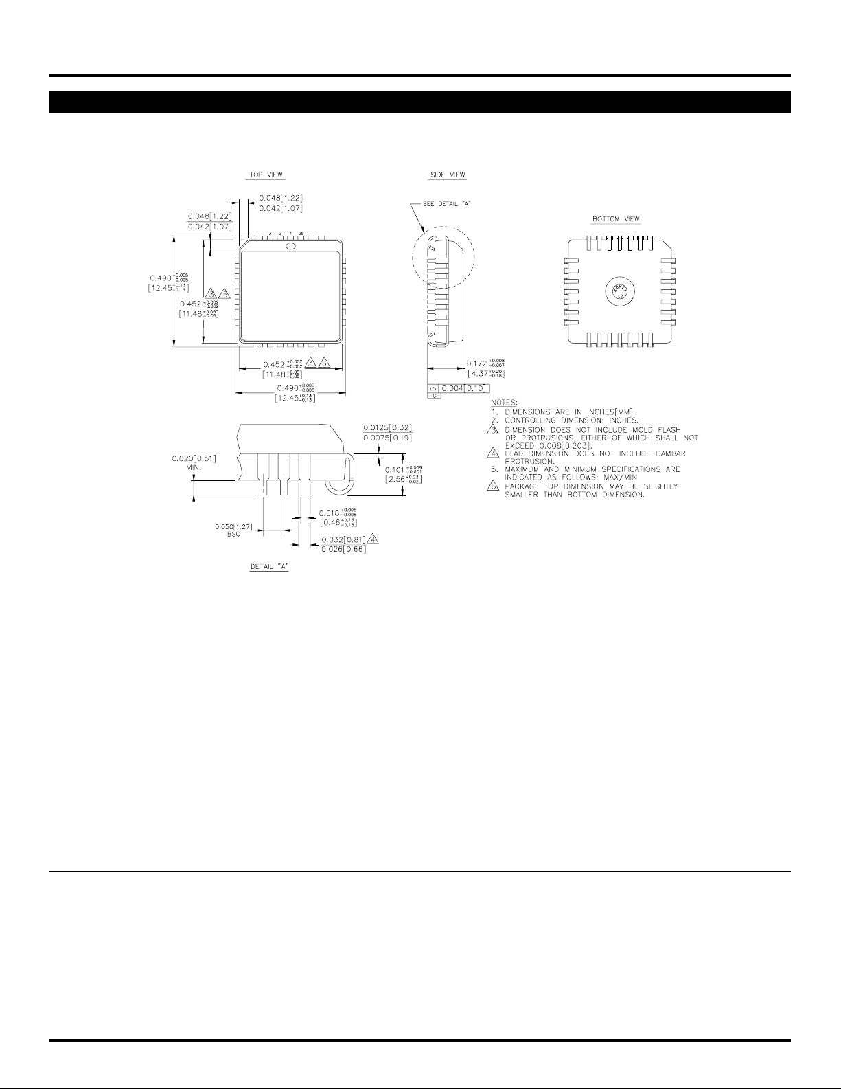
28-PIN PLCC (J28-1)
SY10E137
SY100E137
Rev. 03
MICREL, INC. 2180 FORTUNE DRIVE SAN JOSE, CA 95131 USA
TEL + 1 (408) 944-0800 FAX + 1 (408) 474-1000 WEB http://www.micrel.com
The information furnished by Micrel in this data sheet is believed to be accurate and reliable. However, no responsibility is assumed by Micrel for its use.
Micrel Products are not designed or authorized for use as components in life support appliances, devices or systems where malfunction of a product can
reasonably be expected to result in personal injury. Life support devices or systems are devices or systems that (a) are intended for surgical implant into
the body or (b) support or sustain life, and whose failure to perform can be reasonably expected to result in a significant injury to the user. A Purchaser’s
use or sale of Micrel Products for use in life support appliances, devices or systems is at Purchaser’s own risk and Purchaser agrees to fully indemnify
Micrel reserves the right to change circuitry and specifications at any time without notification to the customer.
Micrel for any damages resulting from such use or sale.
© 2006 Micrel, Incorporated.
M9999-032006
[email protected] or (408) 955-1690
5
 Loading...