

Page 1
■ SILICON EPITA X IAL PLANA R NPN
TRANSISTORS
■ MINIATURE PLASTIC PACKAGE FOR
APPLICAT ION IN SURFACE MOUNT ING
CIRCUITS
■ GENERAL P URPOSE MAINLY INT ENDED
FOR USE IN MEDIUM P OWER INDUSTRIA L
APPLICAT ION AND FOR AUDI O AMP LIFIER
OUTPUT STAGE
■ PNP COMPLEMENTS ARE STZT2907 AND
STZT2907A RESPEC TIVE LY
STZT2222
STZT2222A
MEDIUM POWER AMPLIFIER
ADVANCE DATA
2
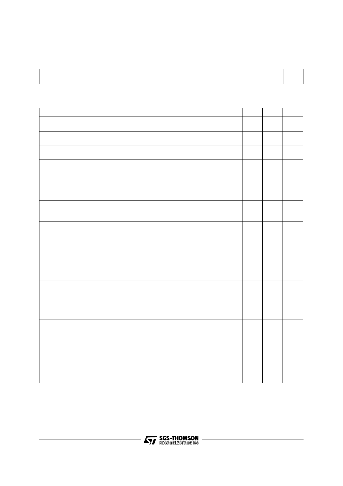
3
2
1
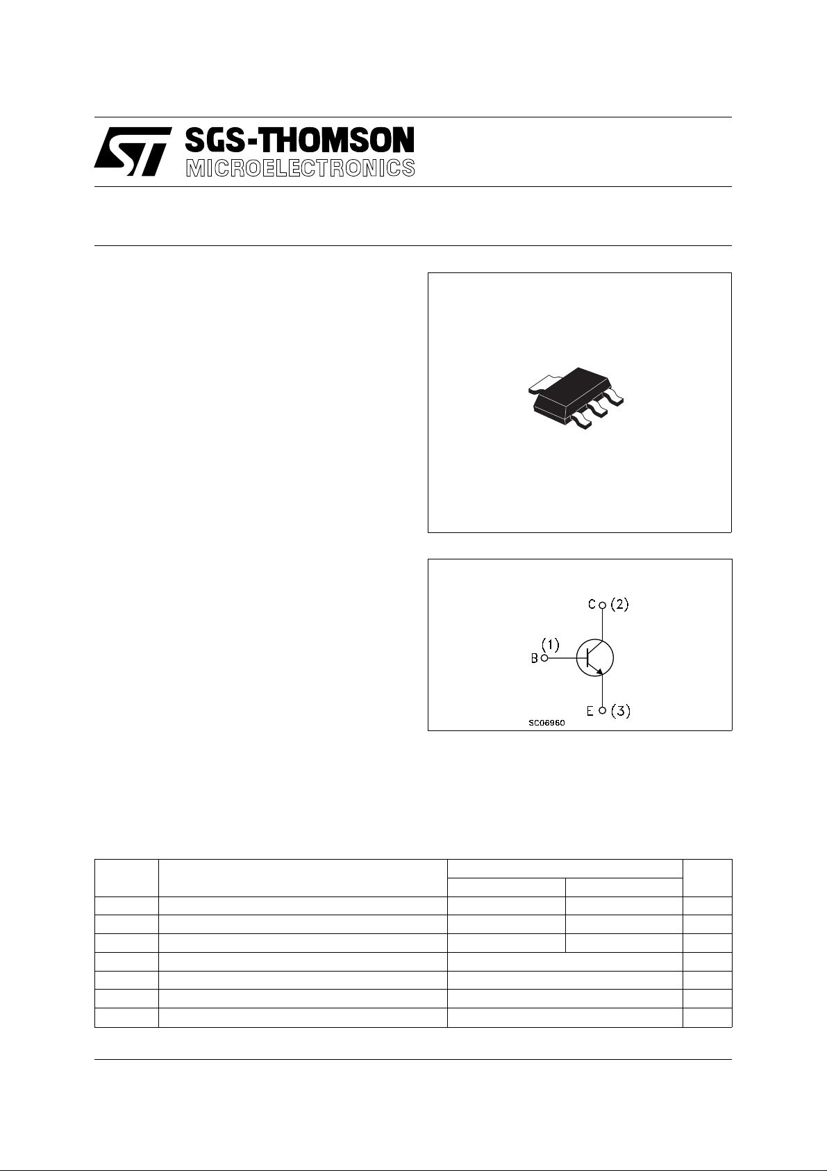
SOT-223
INTERNAL SCHEMATIC DIAGRAM
ABSOLUTE MAXIMUM RATINGS
Symbol Parameter Value Unit
STZT2222 STZT2222A
V
V
V
P
T
Collector-Base Voltage (IE = 0) 60 75 V
CBO
Collector-Emitter Voltage (IB = 0) 30 40 V
CEO
Emitter-Base Voltage (IC = 0) 5 6 V
EBO
Collector Current 0.8 A
I
C
Total Dissipation at Tc = 25 oC 1.5 W
tot
Storage Temperature -65 to 150
stg
Max. Operating Junction Temperature 150
T
j
o
C
o
C
October 1995
1/5
Page 2
STZT2222/STZT2222A
THERMAL DATA
R
R
• Mounted on a ceramic substrate area = 30 x 35 x 0.7 mm
thj-amb
thj-tab
•
Thermal Resistance Junction-Ambient Max
•
Thermal Resistance Junction-Collecor Tab Max
83.3
10
o
C/W
o
C/W
ELECTRICAL CHARACTERISTICS (T
= 25 oC unless otherwise specified)
case
Symbol Parameter Test Conditions Min. Typ. Max. Unit
I
CBO
I
CEX
I
BEX
I
EBO
V
(BR)CBO
V
(BR)CEO
V
(BR)EBO
V
CE(sat)
V
BE(sat)
h
FE
Collector Cut-off
Current (I
= 0)
E
Collector Cut-off
Current (V
= -3V)
BE
Base Cut-off Current
(V
= -3V)
BE
Emitter Cut-off Current
(I
= 0)
E
= rated V
V
CB
VCB = rated V
= 60 V for STZT2222A 10 nA
V
CE
= 60 V for STZT2222A 20 nA
V
CE
= 3 V
V
EB
CBO
CBO
T
amb
for STZT2222
for STZT2222A
Collector-Base
Breakdown Voltage
(IE = 0)
∗ Collector-Emitter
Breakdown Voltage
(I
= 0)
B
Emitter-Base
Breakdown Voltage
(I
= 0)
C
∗ Collector-Emitter
Saturation Voltage
I
= 10 µA
C
for STZT2222
for STZT2222A
I
= 10 mA
C
for STZT2222
for STZT2222A
I
= 10 µA
E
for STZT2222
for STZT2222
IC = 150 mA IB = 15 mA
for STZT2222
for STZT2222A
I
= 500 mA IB = 50 mA
C
for STZT2222
for STZT2222A
∗ Base-Emitter
Saturation Voltage
IC = 150 mA IB = 15 mA
for STZT2222
for STZT2222A
I
= 500 mA IB = 50 mA
C
for STZT2222
for STZT2222A
∗ DC Current Gain IC = 0.1 mA VCE = 10 V
I
= 1 mA VCE = 10 V
C
I
= 10 mA VCE = 10 V
C
I
= 150 mA VCE = 10 V
C
I
= 150 mA VCE = 1 V
C
I
= 500 mA VCE = 10 V
C
for STZT2222
for STZT2222A
I
= 10 mA VCE = 10 V Tc = -55 oC
C
for STZT2222
= 125 oC
60
75
30
40
5
6
35
50
75
100
50
30
40
35
0.6
10
10
30
15
0.4
0.3
1.6
1
1.3
1.2
2.6
2
300
nA
µA
nA
nA
V
V
V
V
V
V
V
V
V
V
V
V
V
V
2/5
Page 3

STZT2222/STZ T2222A
ELECTRICAL CHARACTERISTICS (T
= 25 oC unless otherwise specified)
case
Symbol Parameter Test Conditions Min. Typ. Max. Unit
hfe ∗∗ Small Signal Current
Gain
∗∗ Input Impedance IC = 1 mA VCE = 10 V f = 1 KHz
h
ie
h
∗∗ Reverse Voltage Ratio IC = 1 mA VCE = 10 V f = 1 KHz
re
hoe ∗∗ Output Impedance IC = 1 mA VCE = 10 V f = 1 KHz
f
C
CBO
Transition Frequency IC = 10 mA VCE = 10 V f = 100 MHz
T
Collector-Base
IC = 1 mA VCE = 10 V f = 1 KHz
I
= 10 mA VCE = 10 V f = 1 KHz5075
C
300
375
8
I
= 10 mA VCE = 10 V f = 1 KHz20.25
C
1.25
8
I
= 10 mA VCE = 10 V f = 1 KHz
C
4
35
I
= 10 mA VCE = 10 V f = 1 KHz525
C
for STZT2222
for STZT2222A
250
300
375
IE = 0 VCB = 10 V f = 1 MHz 8 pF
Capacitance
C
EBO
Emitter-Base
Capacitance
NF Noise Figure f = 1 KHz ∆F = 200 Hz R
t
t
∗ Pulsed: Pulse durat ion = 300 µs, dut y cycl e ≤ 1.5 %
∗∗ Only for STZT2222A
Delay Time IC = 150 mA IC1 = 15 mA
d
t
Rise Time 25 ns
r
Storage Time IC = 150 mA IC1 = 15 mA
s
Fall Time 60 ns
t
f
IC = 0 VEB = 0.5 V f = 1 MHz
for STZT2222
for STZT2222A
= 1KΩ
I
= 0.1 mA VCE = 10 V
C
V
= -0.5 V
BE
I
= 15 mA
B2
G
30
25
4dB
10 ns
225 ns
KΩ
10
S
MHz
MHz
pF
pF
-4
3/5
Page 4

STZT2222/STZT2222A
SOT223 MECHANICAL DATA
DIM.
MIN. TYP. MAX. MIN. TYP. MAX.
a 2.27 2.3 2.33 89.4 90.6 91.7
b 4.57 4.6 4.63 179.9 181.1 182.3
c 0.2 0.4 0.6 7.9 15.7 23.6
d 0.63 0.65 0.67 24.8 25.6 26.4
e1 1.5 1.6 1.7 59.1 63 66.9
e4 0.32 12.6
f 2.9 3 3.1 114.2 118.1 122.1
g 0.67 0.7 0.73 26.4 27.6 28.7
l1 6.7 7 7.3 263.8 275.6 287.4
l2 3.5 3.5 3.7 137.8 137.8 145.7
L 6.3 6.5 6.7 248 255.9 263.8
mm mils
L
e1
a
b
f
C
l1
B
C
E
g
d
l2
c
e4
P008B
4/5
Page 5

STZT2222/STZ T 2222A
Information furnished is believed to be accurate and reliable. However, SGS-THOMSON Microelectronics assumes no responsability for the
consequences of use of such information nor for any infringement of pat e nt s or ot her rights of third parties which may results from its use. No
license is granted by implication or otherwise under any patent or patent rights of SG S-THOMSON Microelectroni cs. Specifications ment ioned
in this publication are subject to cha nge wi t hout n o tice. This p u bli ca t ion sup e rsed e s and r epla ces al l inf ormat i on pr ev io us ly supplied.
SGS-THOMSON Microelectronics products are not auth orized for use as critical components in life support devices or systems without express
written approval of SGS-THOM SO N M icroelecto nics.
© 1995 SGS-THOMSON Microelectronics - All Rights Reserved
Australia - Brazil - France - Germany - Hong Ko ng - Ita ly - Japa n - Korea - Mal ay sia - Mal ta - Mor oc co - The Net her l ands -
Singapore - Spain - Sweden - Switzerland - Taiwan - Thailand - United Kingdom - U.S.A
SGS-THOMSON Microelectronics GROUP OF COMPANIES
.
5/5
 Loading...