

Page 1
STY60NM60
N-CHANNEL 600V - 0.050Ω - 60A Max247
Zener-Protected MDmesh™Power MOSFET
TYPE V
STY60NM60 600V < 0.055Ω 60 A
TYPICAL RDS(on) = 0.050Ω
HIGH dv/dt AND AVALANCHE CAPABILITIES
IMPROVED ESD CAPABILITY
LOW INPUT CAPACITANCE AND GATE
DSS
R
DS(on)
I
D
CHARGE
LOW GATE INPUT RESISTANCE
TIGHT PROCESS CONTROL
INDUSTRY’S LOWEST ON-RESISTANCE
DESCRIPTION
The MDmes h™ is a new revolutionary MOSFET
technology that associates the Multiple Drain process with the Company’s Pow erMESH™ horizontal
layout. Theresultingproducthasanoutstanding low
on-resistance, impressively high dv/dt and excellent
avalanche characteristics. The adoption of the
Company’s proprietary strip technique yields overall
dynamic performance that issignificantlybetterthan
that of similar competition’s products.
APPLICATIONS
The MDmesh™ family is very suitable for increasing
power densi ty of high voltage converters allowing
system miniaturization and higher e fficiencies.
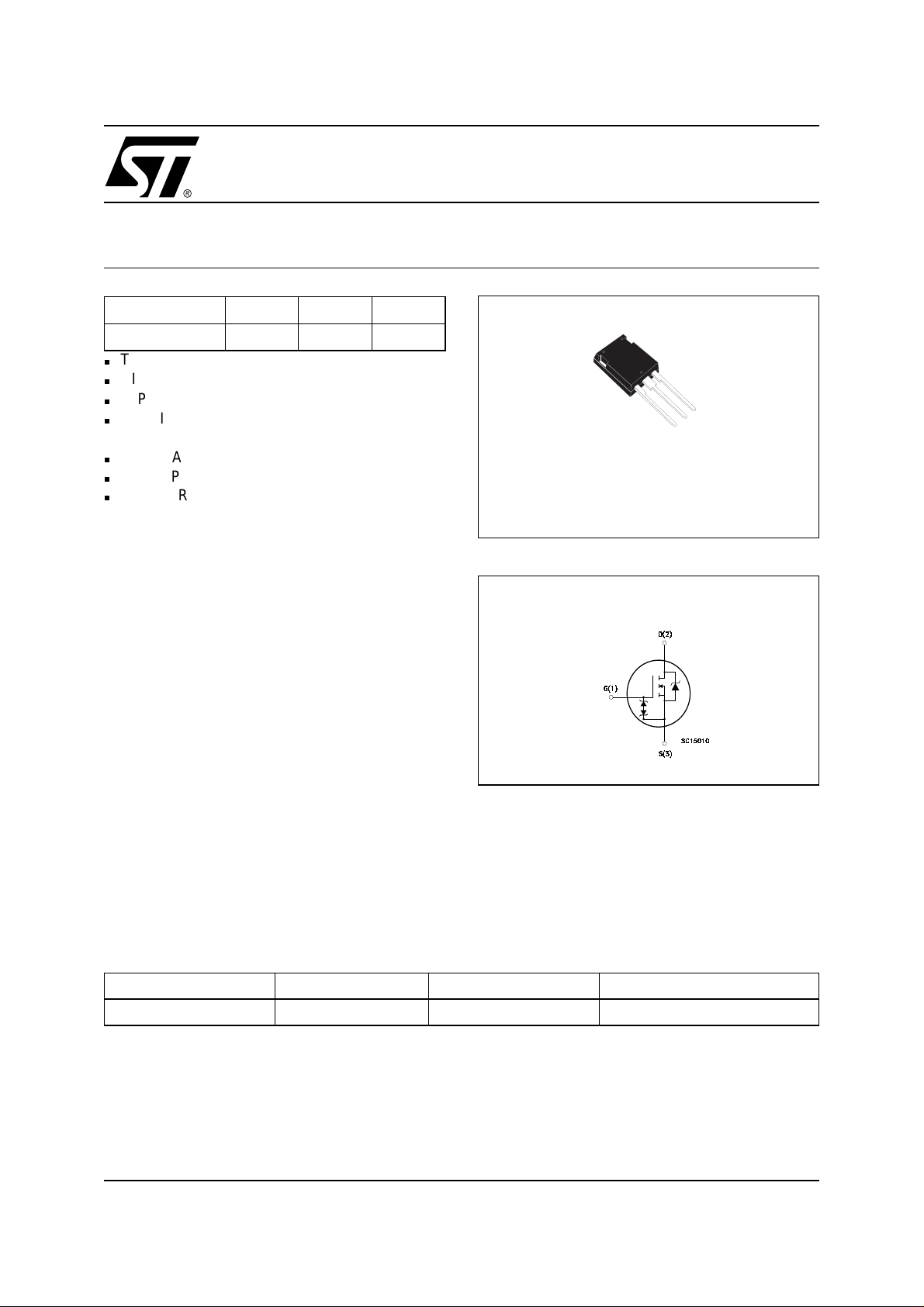
3
2
1
Max247
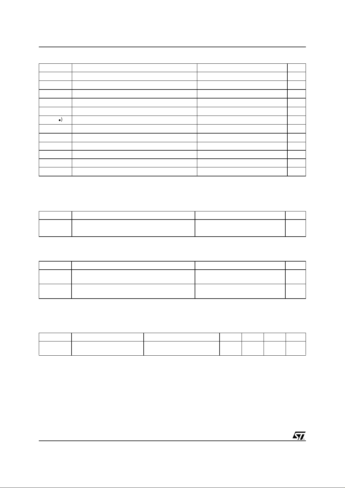
INTERNAL SCHEMATIC DIAGRAM
ORDERING INFORMATION
SALES TYPE MARKING PACKAGE PACKAGING
STY60NM60 Y60NM60 Max247 TUBE
1/8July 2003
Page 2
STY60NM60
ABSOLUTE MAXIMUM RATINGS
Symbol Parameter Value Unit
V
DS
V
DGR
V
GS
I
D
I
D
I
DM
P
TOT
V
ESD(G-S)
dv/dt (1) Peak Diode Recovery voltage slope 15 V/ns
T
stg
T
j
(•)Pulse width limited by safe operating area
≤60A, di/dt ≤400 A/µs, VDD≤ V
(1) I
SD
THERMAL DATA
Rthj-case Thermal Resistance Junction-case Max 0.22 °C/W
Rthj-amb Thermal Resistance Junction-ambient Max 30 °C/W
T
l
Drain-source Voltage (VGS=0)
Drain-gate Voltage (RGS=20kΩ)
600 V
600 V
Gate- source Voltage ±30 V
Drain Current (continuous) at TC= 25°C
Drain Current (continuous) at TC= 100°C
()
Drain Current (pulsed) 240 A
Total Dissipation at TC= 25°C
60 A
37.8 A
560 W
Gate source ESD(HBM-C=100pF, R=15KΩ) 6KV
Derating Factor 4.5 W/°C
Storage Temperature –65 to 150 °C
Max. Operating Junction Temperature 150 °C
(BR)DSS,Tj≤TJMAX.
Maximum Lead Temperature For Soldering Purpose 300 °C
AVALANCHE CHARACTERISTICS
Symbol Parameter Max Value Unit
I
AR
E
AS
Avalanche Current, Repetitive or Not-Repetitive
(pulse width limited by T
max)
j
Single Pulse Avalanche Energy
(starting T
= 25 °C, ID=IAR,VDD=35V)
j
30 A
1.4 J
GATE-SOURCE ZENER DIODE
Symbol Parameter Test Conditions Min. Typ. Max. Unit
BV
GSO
Gate-Source Breakdown
Igs=± 1mA (Open Drain) 30 V
Voltage
PROTECTION FEATURES OF GATE-TO-SOURCE ZENER DIODES
The built-in back -to-back Zener diodes have specifically been des igned to enhance not o nly the device’s
ESD capability, but also to make them safely absorb possibl e voltage transients that may occasionally be
applied from gate to source. In this respect the Zener voltage is appropriate to achieve an ef fi cient and
cost-effective interve nti on to protect the device’s integrity. These integrated Zener diodes thus avoid the
usage of external components.
2/8
Page 3
STY60NM60
ELECTRICAL CHARACTERISTICS (T
= 25 °C UNLESS OTHERWISE SPECIFIED)
CASE
ON/OFF
Symbol Parameter Test Conditions Min. Typ. Max. Unit
V
(BR)DSS
Drain-source
ID= 250 µA, VGS= 0 600 V
Breakdown Voltage
I
DSS
I
GSS
V
GS(th)
R
DS(on)
Zero Gate Voltage
Drain Current (V
GS
=0)
Gate-body Leakage
Current (V
DS
=0)
Gate Threshold Voltage
Static Drain-source On
V
= Max Rating
DS
= Max Rating, TC= 125°C
V
DS
V
= ± 20V ±10 µA
GS
V
DS=VGS,ID
= 250 µA
34
10 µA
100 µA
5V
VGS=10V,ID= 30 A 0.050 0.055 Ω
Resistance
DYNAMIC
Symbol Parameter Test Conditions Min. Typ. Max. Unit
(1) Forward Transconductance VDS=I
g
fs
C
iss
C
oss
C
rss
R
G
Input Capacitance
Output Capacitance
Reverse Transfer
Capacitance
Gate Input Resistance f=1 MHz Gate DC Bias = 0
D(on)xRDS(on)max,
ID=30A
=25V,f=1MHz,VGS= 0 7300
V
DS
Test Signal Level = 20mV
Open Drain
35 S
2000
40
1.8 Ω
pF
pF
pF
SWITCHING ON
Symbol Parameter Test Conditions Min. Typ. Max. Unit
t
d(on)
Turn-on Delay Time
t
r
Rise Time
VDD=300V,ID=30A
= 4.7Ω VGS=10V
R
G
55
95
(see test circuit, Figure 3)
Q
g
Q
gs
Q
gd
Total Gate Charge
Gate-Source Charge
Gate-Drain Charge
VDD=470V,ID=60A,
VGS=10V
178
44.5
95
266 nC
SWITCHING OFF
Symbol Parameter Test Conditions Min. Typ. Max. Unit
t
r(Voff)
t
t
Off-voltage Rise Time
f
c
Fall Time
Cross-over Time
VDD= 400 V, ID=60A,
RG=4.7Ω, VGS=10V
(see test circuit, Figure 5)
130
76
105
SOURCE DRAIN DIODE
Symbol Parameter Test Conditions Min. Typ. Max. Unit
I
SD
I
SDM
VSD(1)
t
rr
Q
rr
I
RRM
Note: 1. Pulsed: Pulse duration = 300 µs, duty cycle 1.5 %.
2. Pulse width limited by safe operating area.
Source-drain Current
Source-drain Current (pulsed)
(2)
Forward On Voltage
Reverse Recovery Time
Reverse Recovery Charge
Reverse Recovery Current
ISD=60A,VGS=0
I
SD
VDD=30V,Tj= 150°C
(see test circuit, Figure 5)
= 60 A, di/dt = 100 A/µs,
600
14
48
60
240
1.5 V
ns
ns
nC
nC
ns
ns
ns
A
A
ns
µC
A
3/8
Page 4

STY60NM60
Safe Operating Area Thermal I mpedance
Output Characteristics
Transconductance
Transfer Characteristics
Static Drain-source On Resistance
4/8
Page 5

STY60NM60
Capacitance VariationsGate Charge vs Gate-source Voltage
Normalized Gate Threshold Voltage vs Temp.
Source-drain Diode Forw ard Characteristics
Normalized On Resistanc e vs Temperature
Normalized BVDSS vs Temperature
5/8
Page 6

STY60NM60
Fig. 2: Unclamped Inductive WaveformFig. 1: Unclamped Inductive Load Test Circuit
Fig. 3: Switching Times Test Circuit For
Resistive Loa d
Fig. 5: Test Circuit For Inductive Load Switching
And Diode Recovery T imes
Fig. 4: Gate Charge te st Circuit
6/8
Page 7

Max247 MECHANI CAL DATA
STY60NM60
DIM.
MIN. TYP. MAX. MIN. TYP. MAX.
A 4.70 5.30
A1 2.20 2.60
b 1.00 1.40
b1 2.00 2.40
b2 3.00 3.40
c 0.40 0.80
D 19.70 20.30
e 5.35 5.55
E 15.30 15.90
L 14.20 15.20
L1 3.70 4.30
mm inch
P025Q
7/8
Page 8

STY60NM60
Information furnished is believed to be accurate and reliable. However, STMicroelectronics assumes no responsibility for the
consequences of u se of such inf ormat ion nor for any in fring ement of p aten ts or othe r ri ghts of th ird p arties whic h may resul t f rom
its use. No license is granted by implication or otherwise under any patent or patent rights of STMicroelectronics. Specifications
mentioned in this publication are subject to change without notice. This publication supersedes and replaces all information
previously supplied. STMicroelectronics products are not authorized for use as critical components in life support devices or
systems without express written approval of STMicroelectronics.
Australia - Brazil - Canada - China - Finland - France - Germany - Hong Kong - India - Israel - Italy - Japan - Malaysia - Malta - Morocco
© The ST logo is a registered trademark of STMicroelectronics
© 2003 STMicroelectronics - Printed in Italy - All Rights Reserved
Singapore - Spain - Sweden - Switzerland - United Kingdom - United States.
STMicroelectronics GROUP OF COMPANIES
© http://www.st.com
8/8
 Loading...