

Page 1
STY25NA60
N - CHANNEL 600V - 0.225Ω - 25 A - Max247
EXSTREMELY LOW GATE CHARGE POWER MOSFET
TYPE V
DSS
R
DS(on)
I
D
ST Y25NA60 600 V < 0.24 Ω 25 A
■ TYPICALR
■ EFFICIENTANDRELIABLEMOUNTING
DS(on)
= 0.225 Ω
THROUGHCLIP
■ ± 30VGATETO SOURCEVOLTAGERATING
■ 100%AVALANCHETESTED
■ LOW INTRINSICCAPACITANCE
■ GATECHARGE MINIMIZED
■ REDUCEDVOLTAGESPREAD
DESCRIPTION
The Max247 package is a new high volume
powerpackage exibitingthe same footprintas the
industry standard TO-247, but designed to accomodate much larger silicon chips, normally suppliedin biggerpackages such as TO-264.Theincreaseddie capacity makes the deviceidealto reduce component count in multiple paralleled designsand save board space with respectto larger
packages.
APPLICATIONS
■ HIGHCURRENT, HIGH SPEED SWITCHING
■ SWITCHMODE POWER SUPPLY (SMPS)
■ DC-AC CONVERTERFOR WELDING
EQUIPMENTAND UNINTERRUPTABLE
POWERSUPPLY AND MOTORDRIVE
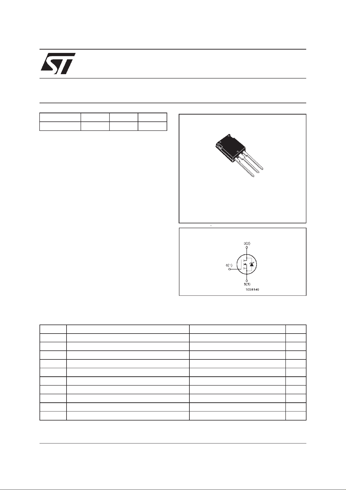
3
2
1
Max247
INTERNAL SCHEMATIC DIAGRAM
ABSOLUTE MAXIMUM RATINGS
Symbol Parameter Value Unit
V
V
V
I
DM
P
T
(•) Pulse width limitedby safeoperating area
March 1999
Drain-source Volta ge (VGS=0) 600 V
DS
Drain- gate Voltage (RGS=20kΩ)
DGR
Gat e-source V oltage ± 30 V
GS
I
Drain Curre nt (cont in uous) at Tc=25oC25A
D
I
Drain Curre nt (cont in uous) at Tc= 100oC 16.5 A
D
600 V
(•) Drain Current (pulsed) 100 A
Tot al Dissipation at Tc=25oC300W
tot
Derating F act or 2.4 W/
Sto rage Tem peratu r e -55 to 150
stg
T
Max. Operati ng J unction Temperatu r e 150
j
o
C
o
C
o
C
1/8
Page 2
STY25NA60
THERMAL DATA
R
thj-case
R
thj-amb
R
thc-sink
AVALANCHE CHARACTERISTICS
Symbol Para meter Max Val ue Uni t
I
AR
E
Ther mal Resistanc e Juncti on-case Max
Ther mal Resistanc e Juncti on-amb ient Max
Thermal Resistance Case-Heatsink Typ
with Cond uctive Greas e
Avalanche Cu r rent, Repetit ive or Not- Re petit ive
(pulse width limited by T
Single Pulse Avalanche En ergy
AS
(starting T
=25oC, ID=IAR,VDD=50V)
j
max)
j
0.42
40
0.05
25 A
3000 mJ
o
C/W
o
C/W
o
C/W
ELECTRICAL CHARACTERISTICS (T
=25oC unless otherwisespecified)
case
OFF
Symbol Parameter Test Conditions Min. Typ. Max. Unit
V
(BR)DSS
Drain-sou rc e
=250µAVGS=0
I
D
600 V
Break d own Voltage
I
DSS
I
GSS
Zero Gate Voltage
Drain Current (V
GS
Gat e- b ody Le akage
Current (V
DS
=0)
=0)
V
=MaxRating
DS
= Max Rating Tc=125oC
V
DS
= ± 30 V
V
GS
50
500
± 100 nA
ON(∗)
Symbol Parameter Test Conditions Min. Typ. Max. Unit
V
GS(th)
Gate Threshold
V
DS=VGSID
= 250 µ A
345V
Voltage
R
DS(on)
Static Drain-source On
VGS=10V ID= 12 . 5 A 0.225 0. 2 4
Resistance
I
D(on)
On State Drain Cur rent VDS>I
D(on)xRDS(on)max
25 A
VGS=10V
DYNAMIC
Symbol Parameter Test Conditions Min. Typ. Max. Unit
g
(∗)Forward
fs
Tr anscond uctance
C
C
C
Input Capaci t an c e
iss
Out put Capacitance
oss
Reverse Transf er
rss
Capacitance
VDS>I
D(on)xRDS(on)maxID
= 12.5 A 20 S
VDS=25V f=1MHz VGS= 0 6200
690
195
µA
µ
Ω
pF
pF
pF
A
2/8
Page 3
STY25NA60
ELECTRICAL CHARACTERISTICS
(continued)
SWITCHINGON
Symbol Parameter Test Conditions Min. Typ. Max. Unit
t
d(on)
Turn-on delay Time
t
Rise Time
r
VDD= 300 V ID= 12.5 A
=4.7 Ω VGS=10V
R
G
45
70
(see te st circuit, fi gure 3)
Q
Q
Q
Total Gate Charge
g
Gat e- Sour ce Cha rge
gs
Gate-Drain Charge
gd
VDD= 480 V ID=25A VGS=10V 240
25
115
315 nC
SWITCHINGOFF
Symbol Parameter Test Conditions Min. Typ. Max. Unit
t
r(Voff)
t
t
Off -voltage Rise T ime
Fall Time
f
Cross-over Ti m e
c
VDD= 480 V ID=25A
=4.7 Ω VGS=10V
R
G
(see te st circuit, fi gure 5)
70
25
105
SOURCEDRAINDIODE
Symbol Parameter Test Conditions Min. Typ. Max. Unit
I
V
I
SDM
SD
Q
I
RRM
SD
t
Source-drain Curr ent
(•)
Source-drain Curr ent
25
100
(pulsed)
(∗) For ward On Volt age ISD=25A VGS=0 2 V
Reverse Recovery
rr
Time
Reverse Recovery
rr
=25A di/dt=100A/µs
I
SD
= 100 V Tj=150oC
V
DD
(see te st circuit, fi gure 5)
840
19.5
Charge
Reverse Recovery
46.5
Current
ns
ns
nC
nC
ns
ns
ns
A
A
ns
µ
A
C
(∗) Pulsed:Pulse duration = 300 µs, duty cycle 1.5%
(•) Pulse width limited by safeoperatingarea
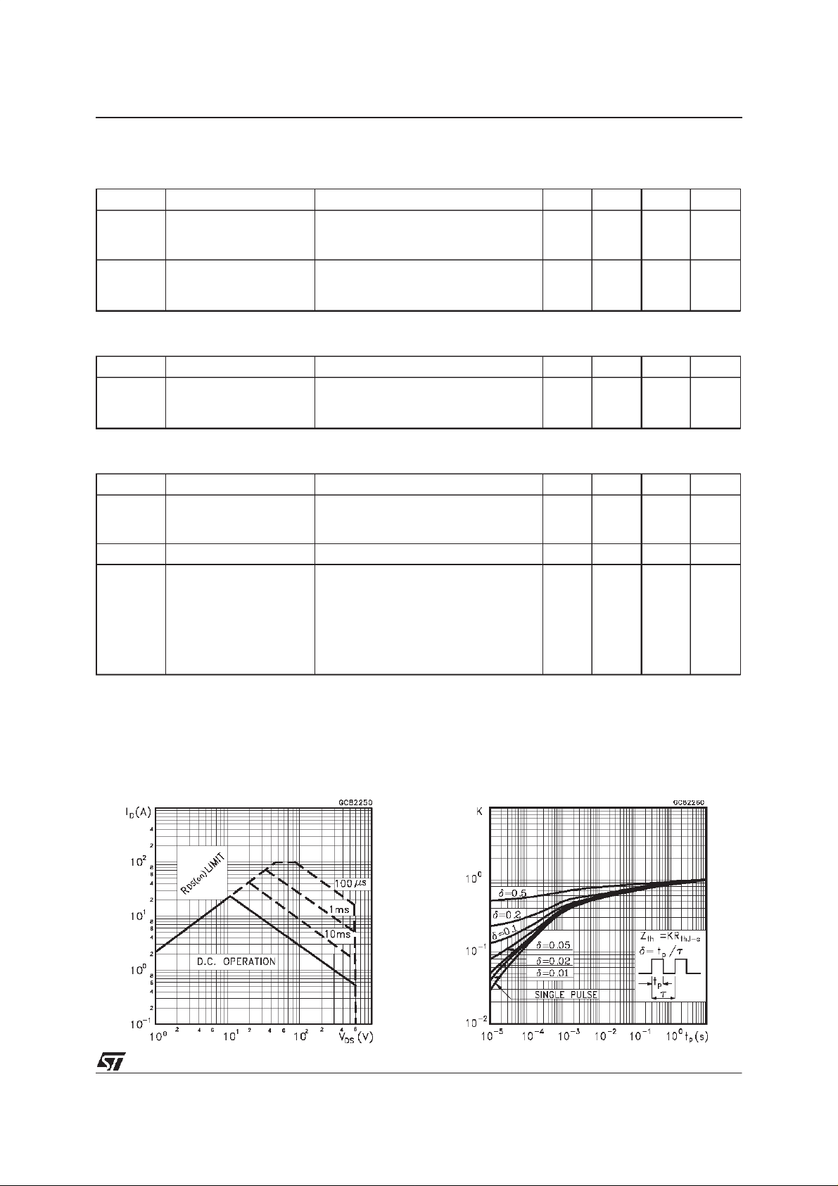
SafeOperating Area ThermalImpedance
3/8
Page 4

STY25NA60
OutputCharacteristics
Transconductance
TransferCharacteristics
Static Drain-sourceOn Resistance
Gate Charge vs Gate-sourceVoltage
4/8
CapacitanceVariations
Page 5

STY25NA60
Normalized Gate ThresholdVoltagevs
Temperature
Source-drainDiode Forward Characteristics
Normalized On Resistancevs Temperature
5/8
Page 6

STY25NA60
Fig. 1:
UnclampedInductiveLoad TestCircuit
Fig. 3: SwitchingTimes Test CircuitsFor
ResistiveLoad
Fig. 2:
UnclampedInductive Waveform
Fig. 4: Gate Charge test Circuit
Fig. 5:
Test CircuitFor InductiveLoad Switching
And Diode Recovery Times
6/8
Page 7

Max247 MECHANICAL DATA
STY25NA60
DIM.
MIN. TYP. MAX. MIN. TYP. MAX.
A 4.70 5.30
A1 2.20 2.60
b 1.00 1.40
b1 2.00 2.40
b2 3.00 3.40
c 0.40 0.80
D 19.70 20.30
e 5.35 5.55
E 15.30 15.90
L 14.20 15.20
L1 3.70 4.30
mm inch
P025Q
7/8
Page 8

STY25NA60
Information furnished is believed tobeaccurateand reliable. However, STMicroelectronics assumes no responsibilityfor the consequences
of use of such information nor for any infringement of patents or other rights of third parties which may result from its use. No license is
granted by implication orotherwise under any patent or patent rights of STMicroelectronics. Specificationmentioned in this publication are
subjecttochange without notice. This publication supersedes and replaces all information previouslysupplied. STMicroelectronicsproducts
are not authorized for use as critical components in life support devices or systemswithout express written approval ofSTMicroelectronics.
The STlogo is a trademark of STMicroelectronics
1999 STMicroelectronics – Printed in Italy – All Rights Reserved
STMicroelectronics GROUP OF COMPANIES
Australia - Brazil - Canada - China - France - Germany - Italy - Japan- Korea - Malaysia - Malta- Mexico - Morocco - The Netherlands -
8/8
Singapore - Spain - Sweden - Switzerland - Taiwan - Thailand - United Kingdom - U.S.A.
http://www.st.com
.
 Loading...