

Page 1
STY16NA90
N - CHANNEL 900V - 0.5 Ω - 16A - Max247
EXTREMELY LOW GATE CHARGE POWER MOSFET
PRELIMINARY DATA
TYPE V
DSS
ST Y16NA90 900 V < 0. 54 Ω 16 A
R
DS(on)
I
D
■ TYPICALR
■ EFFICIENTANDRELIABLEMOUNTING
DS(on)
=0.5 Ω
THROUGH CLIP
■ ± 30V GATE TO SOURCE VOLTAGERATING
■ REPETITIVEAVALANCHE TESTED
■ LOW INTRINSIC CAPACITANCE
■ 100% AVALANCHETESTED
■ GATECHARGEMINIMIZED
■ REDUCEDTHRESHOLD VOLTAGESPREAD
DESCRIPTION
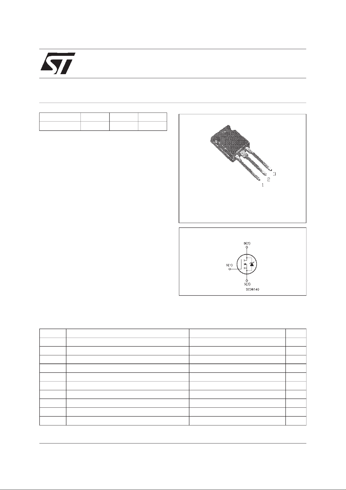
The Max247TMpackage is a new high v olu m e
powe r pac k age ex ibi t ing t he sam e fo ot p rint a s the
indus t r y st andard T O-247, but desi gned to
accomodat e m uch larger s ilicon c hips, normally
suppl ied in bigger packages such as TO-26 4. The
increased die capacity makes the device ideal to
reduce component c ou nt in multiple par a llele d
designs and save board sp ace with respect t o
larger packages .
APPLICATIONS
■ HIGH CURRENT, HIGHSPEEDSWITCHING
■ SWITCHMODEPOWER SUPPLIES(SMPS)
■ DC-ACCONVERTERS FOR WELDING
EQUIPMENTAND UNINTERRUPTIBLE
POWERSUPPLIES (UPS)
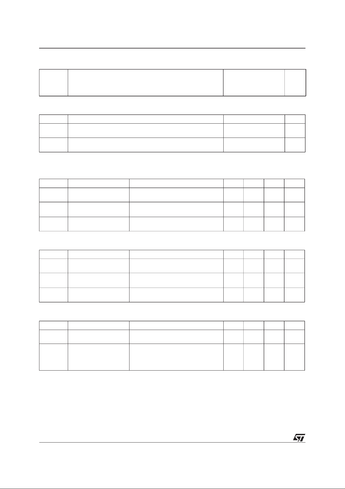
Max247
TM
INTERNAL SCHEMATIC DIAGRAM
ABSOLUTE MAXIMUM RATINGS
Symbol Parameter Value Unit
V
V
DGR
V
I
DM
P
T
(•) Pulse width limitedby safe operating area
June 1998
Drain-s ou r ce V oltage (VGS= 0) 900 V
DS
Drain- gat e V oltage (RGS=20kΩ)
Gate-source Voltage ± 30 V
GS
I
Drain Current (continuous) at Tc=25oC16A
D
I
Drain Current (continuous) at Tc=100oC10A
D
900 V
(•) Drain Current (pulsed) 64 A
Tot al Dissipa t io n at Tc=25oC 300 W
tot
Derating Fact or 2.4 W/
Storage Temperature -55 to 150
stg
T
Max. Ope rating Jun ct io n T emperature 150
j
o
C
o
C
o
C
1/5
Page 2
STY16NA90
THERMAL DATA
R
thj-case
R
thj-amb
R
thc-sin k
AVALANCHE CHARACTERISTICS
Symbol Para met e r Max Value Uni t
I
AR
E
Ther mal Resist ance Junctio n-case Max
Ther mal Resist ance Junctio n-ambient Max
Ther mal Resist ance Case-Heat s ink Typ
with Conduct iv e Grease
Avalanche C ur rent, Rep et it i v e o r Not- Re petitive
(pulse width limited by T
Single Pulse Avalanche Energy
AS
(starting T
=25oC, ID=IAR,VDD=50V)
j
max)
j
0.42
40
0.05
16 A
3000 mJ
o
C/W
o
C/W
ELECTRICAL CHARACTERISTICS (T
=25oC unlessotherwise specified)
case
OFF
Symbol Parameter Test Cond itions Min. Typ. Max. Unit
V
(BR)DSS
Drain-sourc e
=250µAV
I
D
GS
=0
900 V
Breakdown Voltage
I
I
DSS
GSS
Zer o G at e V o lt age
Drain Curre nt ( V
GS
Gat e-body Leak a ge
Current (V
DS
=0)
=0)
V
=MaxRating
DS
=MaxRating Tc=125oC
V
DS
= ± 30 V
V
GS
50
500
± 100 nA
ON (∗)
Symbol Parameter Test Cond itions Min. Typ. Max. Unit
V
GS(th )
Gate Threshold
V
DS=VGSID
=250µA
2.25 3 3.75 V
Voltage
R
DS(on)
Stati c D rain-source On
VGS=10V ID=8A 0.5 0.54 Ω
Resistance
I
D(on)
On Stat e Dra in Curr e nt VDS>I
D(on)xRDS(on)max
16 A
VGS=10V
DYNAMIC
Symbol Parameter Test Cond itions Min. Typ. Max. Unit
g
(∗)Forward
fs
Tr ansconductanc e
C
C
C
Input Ca pac i t an c e
iss
Out put C apa c itance
oss
Reverse T ransfer
rss
Capa cit an c e
VDS>I
D(on)xRDS(on)maxID
=8A 15 S
VDS=25V f=1MHz VGS= 0 6400
600
150
8300
750
200
µA
µA
Ω
pF
pF
pF
2/5
Page 3

STY16NA90
ELECTRICAL CHARACTERISTICS (continued)
SWITCHINGON
Symbol Parameter Test Cond itions Min. Typ. Max. Unit
t
d(on)
Q
Q
Q
Turn-on Tim e
Rise T im e
t
r
Total Gate Charge
g
Gat e-Sour ce Charge
gs
Gate-Drain Charge
gd
VDD=450V ID=8A
=4.7 Ω VGS=10V
R
G
VDD=720V ID=16A VGS= 10 V 245
SWITCHINGOFF
Symbol Parameter Test Cond itions Min. Typ. Max. Unit
t
r(Voff)
t
Of f - voltage Ris e Time
t
Fall Time
f
Cross-ov er T ime
c
VDD=720V ID=16A
=4.7 Ω VGS=10V
R
G
SOURCE DRAIN DIODE
Symbol Parameter Test Cond itions Min. Typ. Max. Unit
I
SD
I
SDM
V
SD
t
Q
I
RRM
(∗) Pulsed: Pulse duration =300 µs, duty cycle1.5 %
(•) Pulse width limited by safe operating area
Source-drain Cu rrent
(•)
Source-drain Cu rrent
(pulsed)
(∗) For ward On Vo lt age ISD=16A VGS=0 2 V
Reverse Recovery
rr
Time
Reverse Recovery
rr
= 16 A di/dt = 100 A/µs
I
SD
=100V Tj=150oC
V
DD
Charge
Reverse Recovery
Current
30
30
25
110
80
25
115
1100
25.3
46
320 nC
105
35
150
16
64
ns
ns
nC
nC
ns
ns
ns
A
A
ns
µC
A
3/5
Page 4

STY16NA90
Max247 MECHANICAL DATA
DIM.
MIN. TYP. MAX. MIN. TYP. MAX.
A 4.70 5.30
A1 2.20 2.60
b 1.00 1.40
b1 2.00 2.40
b2 3.00 3.40
c 0.40 0.80
D 19.70 20.30
e 5.35 5.55
E 15.30 15.90
L 14.20 15.20
L1 3.70 4.30
mm inch
4/5
P025Q
Page 5

STY16NA90
Information furnished is believed tobe accurate and reliable. However, STMicroelectronicsassumes no responsibility for theconsequences
of use of such information nor for any infringement of patents or other rights of third parties which may result from its use. No license is
granted by implication orotherwise under any patent or patent rights of STMicroelectronics. Specification mentionedin this publication are
subject tochange without notice. This publication supersedes and replaces all information previouslysupplied.STMicroelectronics products
are not authorized for use as critical componentsin life support devices or systems without express written approval of STMicroelectronics.
Australia - Brazil - Canada- China - France- Germany- Italy - Japan- Korea - Malaysia - Malta - Mexico- Morocco- The Netherlands -
Singapore- Spain- Sweden- Switzerland- Taiwan -Thailand - United Kingdom- U.S.A.
The ST logo isa trademarkof STMicroelectronics
1998 STMicroelectronics– Printed in Italy– All Rights Reserved
STMicroelectronicsGROUP OFCOMPANIES
.
5/5
 Loading...