

Page 1
Features
■ TO-92 PACKAGE SUITABLE FOR
THROUGH-HOLE PCB ASSEMBLY
Applications
■ VOLTAGE REGULATION
■ RELAY DRIVER
■ GENERIC SWITCH
Description
STX826
PNP MEDIUM POWER TRANSISTOR
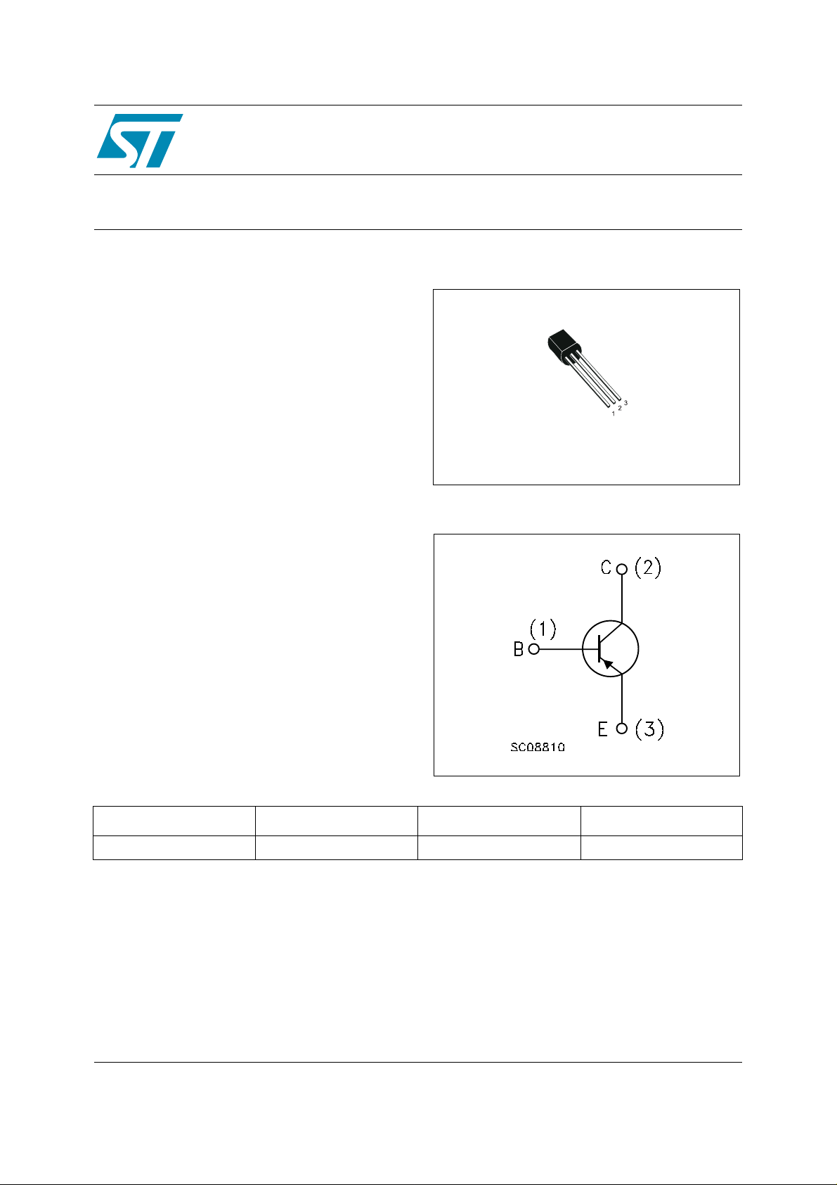
TO-92
The STX826 is PNP transistor manufactured
using planar Technology resulting in rugged high
performance devices.
Internal Schematic Diagram
Order codes
Part Number Marking Package Packing
STX826 X826 TO-92 BULK
Rev 2
October 2005 1/9
www.st.com
9
Page 2
1 Electrical Ratings STX826
1 Electrical Ratings
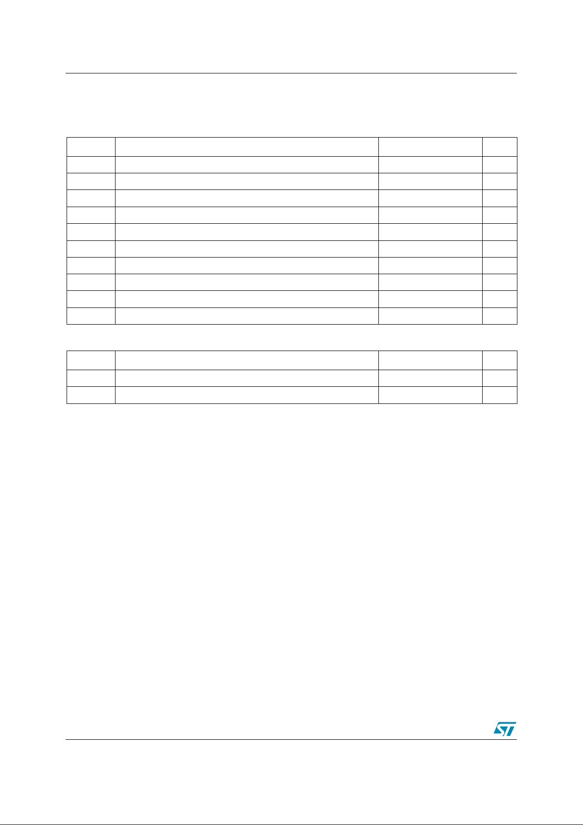
Table 1. Absolute Maximum Rating
Symbol Parameter Value Unit
V
V
V
P
T
CBO
CEO
EBO
I
I
CM
I
I
BM
TOT
STG
T
Collector-Base Voltage (IE = 0)
Collector-Emitter Voltage (IB = 0)
Collector-Base Voltage (IC = 0)
Collector Current -3 A
C
Collector Peak Current (tP < 5ms)
Base Current -1 A
B
Base Peak Current (tP < 5ms)
Total di ssipation at Tc = 25°C
-60 V
-30 V
-5 V
-6 A
-2 A
0.9 W
Storage Temperature -65 to 150 °C
Max. Operating Junction Temperature 150 °C
J
Table 2. Thermal Data
Symbol Parameter Value Unit
R
thJ-case
R
thJ-amb
Thermal Resistance Junction-Case____________________Max 44.6 °C/W
Thermal Resistance Junction-ambi ent _________________Max 139 °C/W
2/9
Page 3
STX826 2 Electrical Char acteristics
2 Electrical Characteristics
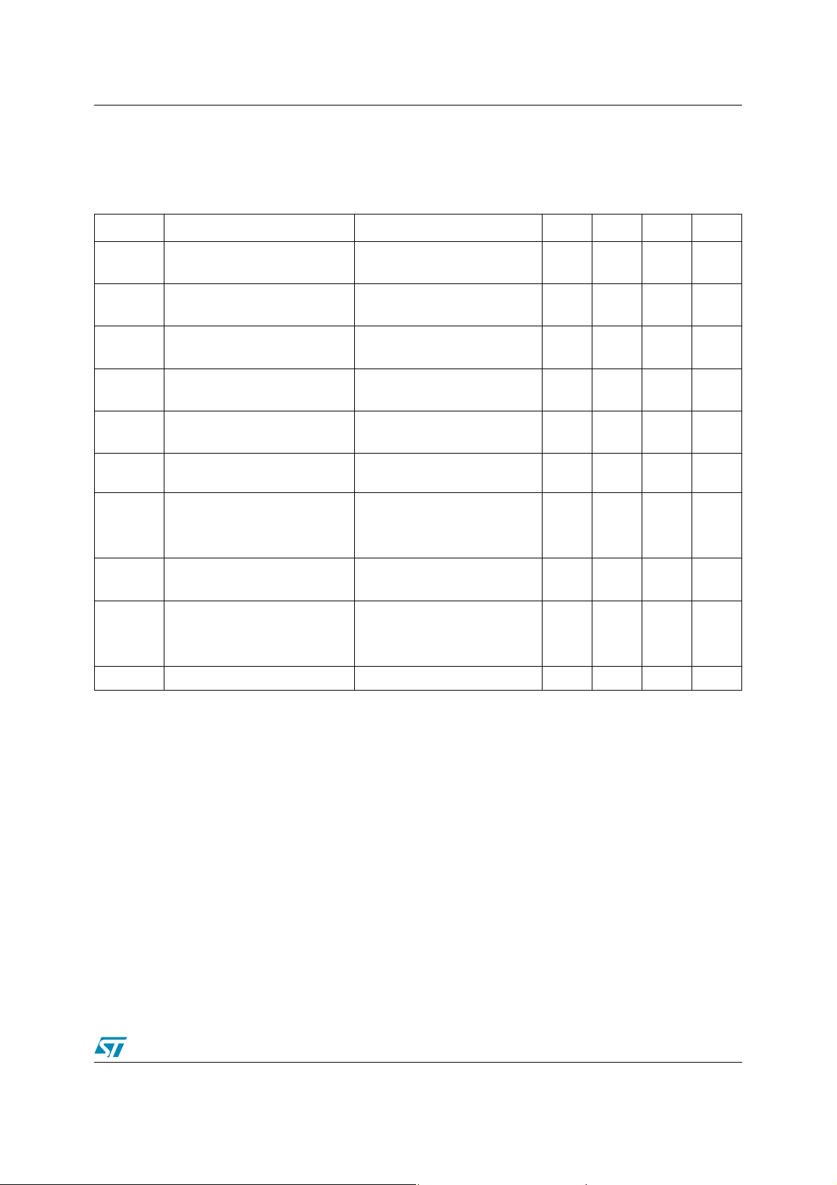
Table 3. Electrical Characteristics (T
= 25°C; unless otherwise specified)
CASE
Symbol Parameter T est Conditions Min. Typ. Max. Unit
I
CES
I
CEO
I
EBO
V
(BR)CBO
V
(BR)CEO
Note: 1
V
(BR)EBO
V
CE(sat)
Note: 1
V
BE(sat)
Note: 1
h
FE
f
T
Collector Cut-off Current
= 0)
(V
BE
Collector Cut-off Current
= 0)
(I
B
Emitter Cut-off Current
= 0)
(I
C
Collector-Base
Breakdown Voltage (I
= 0)
E
Collector-Emit ter Breakdown
Voltage (I
= 0)
B
Collector-Emit ter Breakdown
Voltage (I
= 0)
C
Collector-Emitter Saturation
Voltage
Base-Emitter Saturation Voltage
DC Current Gain
Transistor Frequency
V
= -60V -10 μA
CE
V
= -30V -100 μA
CE
V
= -5V -10 μA
EB
I
= -100μA-60V
C
= -10 mA -30 V
I
C
= -100 μA-5 V
I
E
I
= -1 A IB = -50 A
C
I
= -2 A IB = -100 A
C
I
= -3 A IB = -150 A
C
= -2 A IB = -100 mA -1.2 V
I
C
I
= -100 mA V
C
I
= -1 A V
C
= -3 A V
I
C
V
= -10 V Ic= - 0.1 A 100 MHz
CE
CE
CE
CE
= -2 V
= -2 V
= -2 V
100
80
30
-0.4
-0.7
-1.1
300
V
V
V
Note: 1 Pulsed duration = 300 μs, duty cycle ≤1.5%.
3/9
Page 4
2 Electrical Characteristics STX826
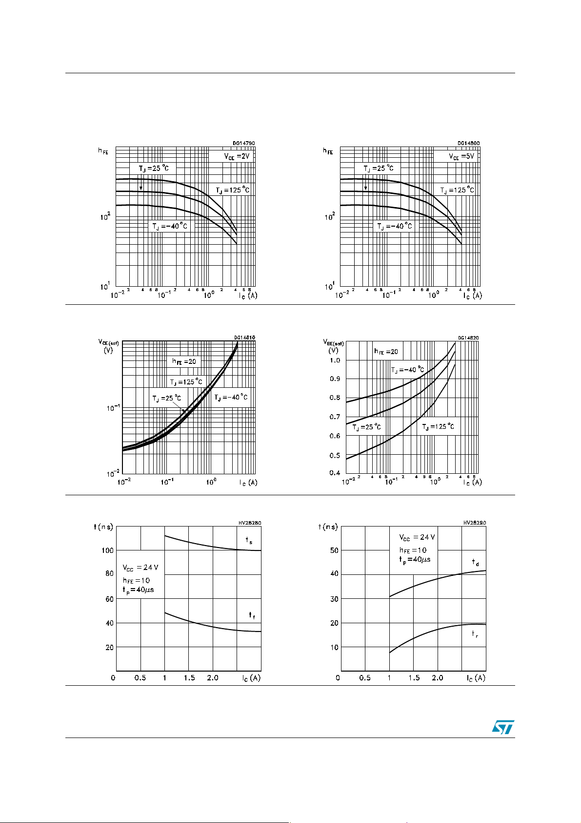
2.1 Electrical characteristics (curve)
Figure 1. DC Current Gain Figure 2. DC Current Gain
Figure 3. Collector-emitter saturation voltage Figure 4. Base-emitter saturation voltage
Figure 5. Switching times on resistive load Figure 6. Switching times resistive on load
4/9
Page 5
STX826 2 Electrical Char acteristics
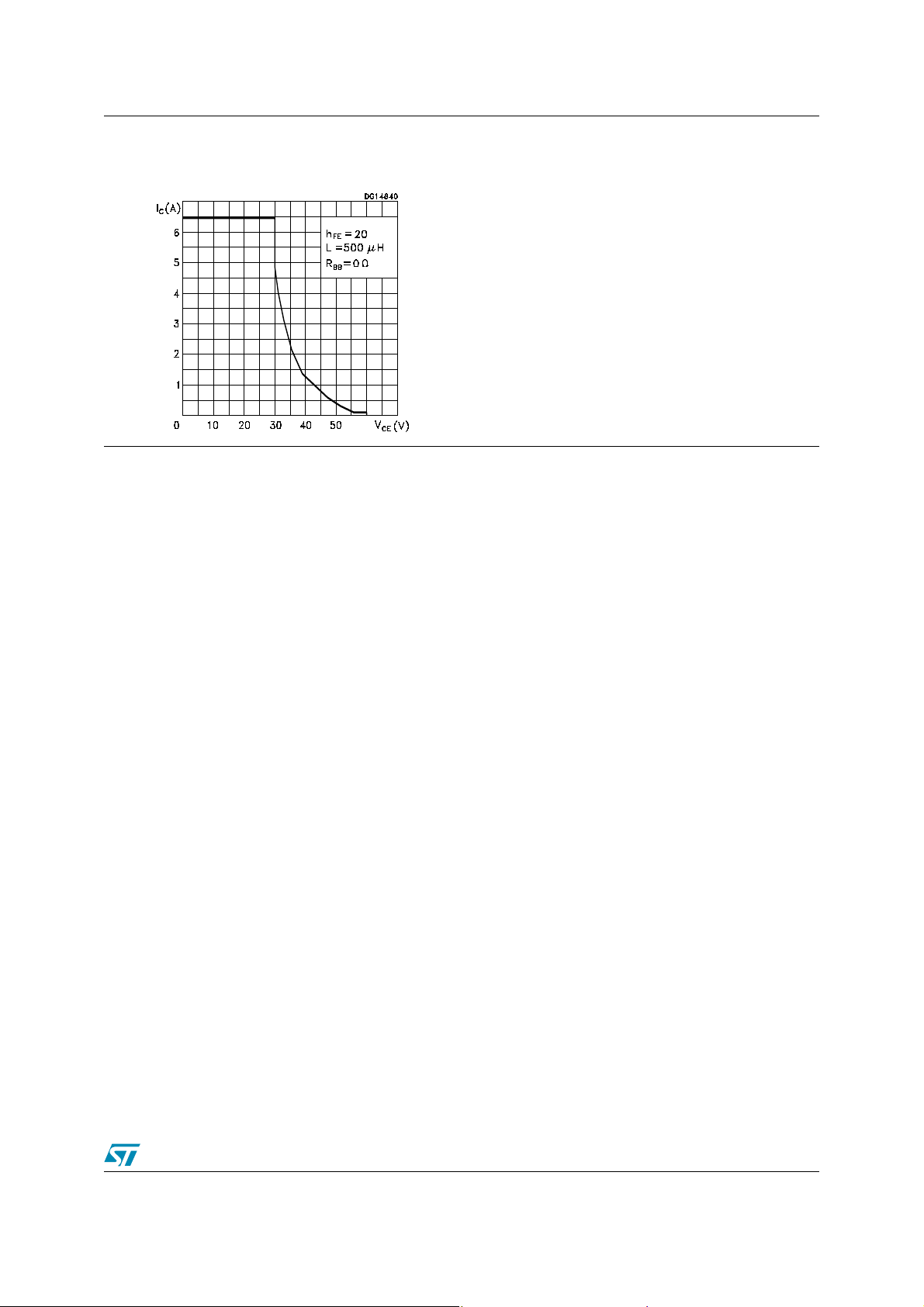
Figure 7. Reverse biased area
5/9
Page 6

3 Package Mechani cal Data STX826
3 Package M echanical Da ta
In order to meet environmental requirements, ST offers these devices in ECOPACK®
packages. These packages have a Lead-free second level interconnect . The category of
second level interconnect is marked on the package and on the inner box label, in compliance
with JEDEC Standard JESD97. The maximum ratings related to soldering conditions are also
marked on the inner box label. ECOPACK is an ST trademark. ECOPACK specifications are
available at: www.st.com
6/9
Page 7
STX826 3 Package Mechanical Data
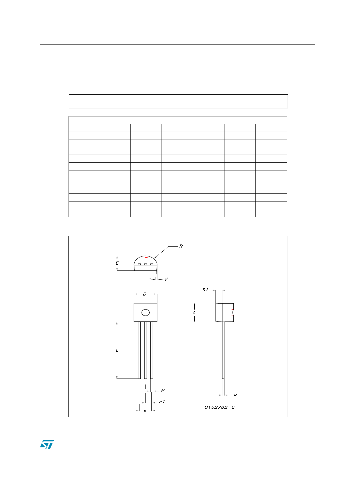
TO-92 MECHANICAL DATA
DIM.
A 4.32 4.95 0.170 0.194
b 0.36 0.51 0.014 0.020
D 4.45 4.95 0.175 0.194
E 3.30 3.94 0.130 0.155
e 2.41 2.67 0.094 0.105
e1 1.14 1.40 0.044 0.055
L 12.70 15.49 0.50 0.610
R 2.16 2.41 0.085 0.094
S1 0.92 1.52 0.036 0.060
W 0.41 0.56 0.016 0.022
V5° 5°
MIN. TYP MAX. MIN. TYP. MAX.
mm. inch
7/9
Page 8
4 Revision Hist ory STX826
4 Revision History
Date Revision Changes
18-Oct-2005 2 Inserted cur ves
8/9
Page 9

STX826 4 Revision History
I
s
o
d
b
ct
t
ot
a
nformation furnished is believed to be accurate and reliable. However, STMicroelectronics assumes no responsibility for the consequence
f use of such information nor for any infringement of patents or other rights of third parties which may result from its use. No license is grante
y implic ation or otherwise u nder any pat ent or pat ent rights of STMicroelectronics. Spec i fications mentioned i n this publication are subje
o change without notice. This publication supersedes and replaces all information previously supplied. STMicroelectronics products are n
uthoriz ed for use as critical compo nents in life support devic es or systems without express written approval of STM i croelect ronics.
The ST logo is a registered t rademark of ST M i croelectr onics.
All other nam es are the pro perty of their respectiv e owners
© 2005 STMi croelectronics - All rights reserved
Austra l i a - Be l gi um - Brazil - Canada - China - Czech Rep ubl i c - Finland - F rance - Germ any - Hong Kon g - India - Israe l - It aly - Japan -
Malaysi a - M al ta - Morocco - Singapore - Spain - Swed en - Switze rl and - United Kingdom - Unit ed States of America
STMicroelectron ics group of com panies
www.st.com
9/9
 Loading...