

Page 1
HIGH VOLTAGE FAST-SWITCHING
Ordering Code Marking Shipment
STX13005
STX13005-AP
■ HIGH VOLTAGE CAPABILITY
■ LOW SPREAD OF DYNAMIC PARAMETERS
■ MINIMUM LOT-TO-LOT SPREAD FOR
RELIABLE OPERATION
■ VERY HIGH SWITCHING SPEED
X13005
X13005
Bulk
Ammopack
STX13005
STX13005-AP
NPN POWER TRANSISTOR
APPLICATIONS:
■ COMPACT FLUORESCENT LAMPS (CFLS)
■ SWITCH MODE POW ER SUPPLIES (AC / DC
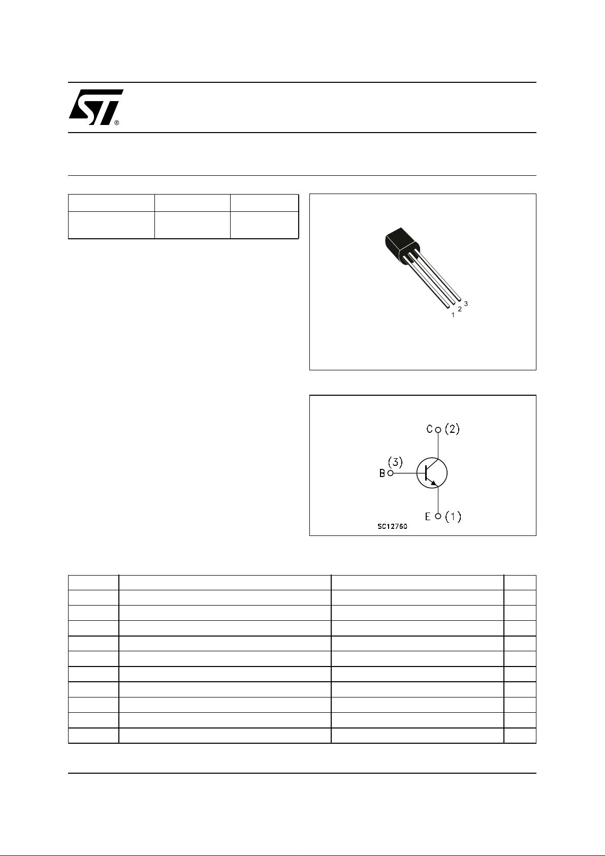
TO-92
CONVERTERS)
DESCRIPTION
The device is manu fac tur ed using Hig h V olt age
Multi Epitaxial Planar technology for h igh switching
INTERNAL SCHE MATIC DIAGRAM
speeds and high voltage capability.
It uses a Cellular Emitter structure with planar edge
termination to enhance switching speeds while
maintaining a wide RBSOA.
ABSOLUTE MAXIMUM RATINGS
Symbol Parameter Value Unit
V
CES
V
CEO
V
EBO
I
I
CM
I
I
BM
P
T
stg
T
Collector-Emitter Voltage (VBE=0)
Collector-Emitter Voltage (IB=0)
Emitter-Base Voltage (IC=0,IB< 1.5 A, tp< 10 ms) V
Collector Current 3 A
C
Collector Peak Current (tp< 5 ms)
Base Current 1.5 A
B
Base Peak Current (tp< 5 ms)
Total Dissipation at Tc=25°C
tot
Storage Temperature –65 to 150 °C
Max. Operating Junction Temperature 150 °C
j
700 V
400 V
(BR)EBO
6A
3A
2.8 W
V
1/8November 2002
Page 2
STX13005 / STX13005- AP
THERMAL DATA
R
thj-case
R
thj-amb
Thermal Resistance Junction-case
Thermal Resistance Junction-ambient
Max
Max
44.6
150
°C/W
°C/W
ELECTRICAL CHARACTE RISTICS (T
= 25 °C unless otherwise spec ified)
j
Symbol Parameter Test Conditions Min. Typ. Max. Unit
I
CES
I
CEO
V
(BR)EBO
Collector Cut-off
Current (V
BE
=0)
Collector Cut-off
Current (I
B
=0)
Emitter-Base
V
= 700 V
CE
VCE= 700 V
V
= 400 V 1 mA
CE
=10mA 9 18 V
I
E
=100°C
T
j
1
5
Breakdown Voltage
=0)
(I
C
V
CEO(sus)
* Collector-Emitter
I
= 10 mA 400 V
C
Sustaining Voltage
=0)
(I
B
* Collector-Emitter
V
CE(sat)
Saturation Voltage
* Base-Emitter
V
BE(sat)
Saturation Voltage
hFE* DC Current Gain IC=1A
RESISTIVE LOAD
s
f
Storage Time
Fall Time
t
t
INDUCTIVE LOAD
s
f
Storage Time
Fall Time
t
t
IC=1A
IC=2A
I
=3A
C
IC=1A
=2A
I
C
=2A
I
C
IC=2A
I
=-IB2= 400 mA
B1
(See Figure 1)
IC=1A
= 200 mA
I
B1
L = 50 mH
=200mA
I
B
IB=500mA
I
=750mA
B
I
=200mA
B
=500mA
I
B
V
=5V
CE
=5V
V
CE
= 125 V
V
CC
t
=30µs
p
V
= 300 V
clamp
=-5V
V
BE(off)
R
=0
BB
10
0.5
0.6
5
1.2
1.6
30
8
24
1.65
260
0.8
150
(See Figure 2)
* Pulsed:Pulse duration= 300 µs,duty cycle=1.5 %.
mA
mA
V
V
V
V
V
µs
ns
µs
ns
2/8
Page 3
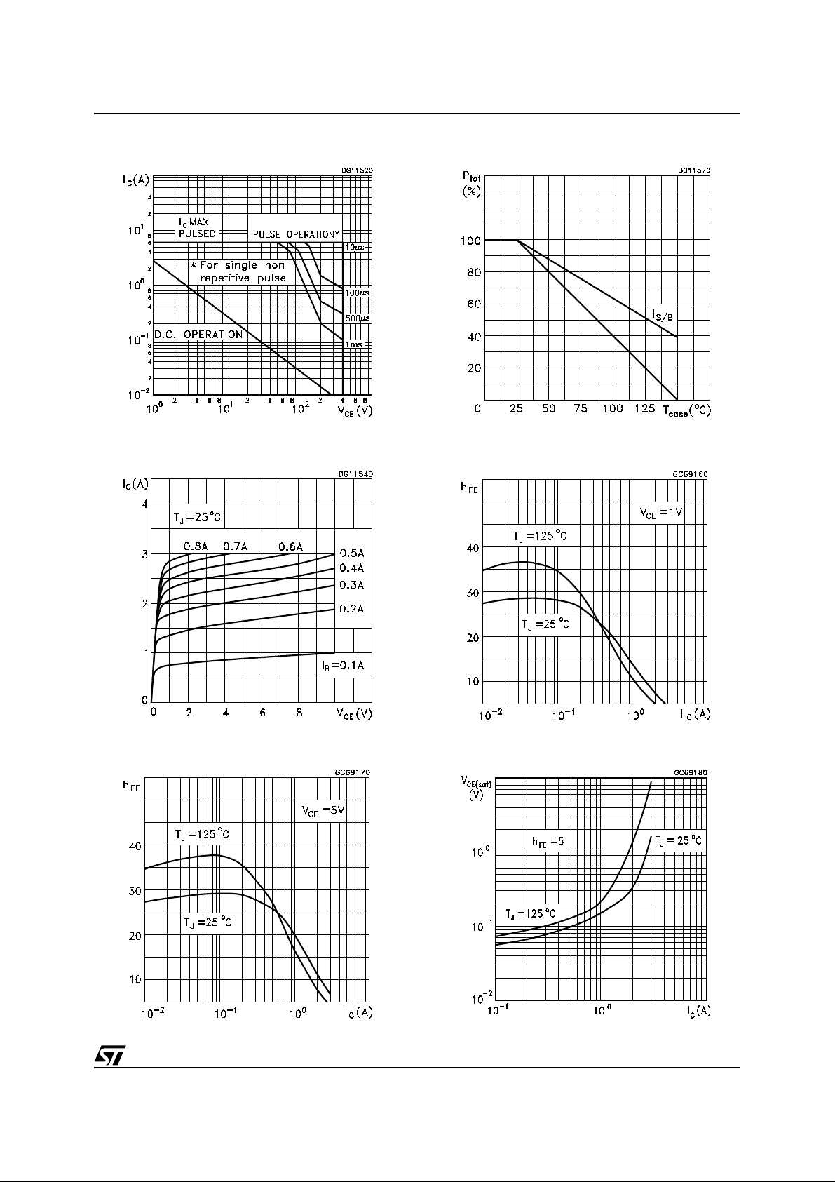
Safe Operating Area Derating Curve
DC Cu rrent GainOutput Characteristics
STX13005 / STX13005- A P
DC Current Gain
Collector-Emitter Saturation Voltage
3/8
Page 4

STX13005 / STX13005- AP
Base-Emitter Saturation Voltage
Resistive Load Fall Time
Resistive Load Storage Time
Inductive Load Storage Time
Inductive Load Fall Time Reverse Biased S afe Operat ing Area
4/8
Page 5
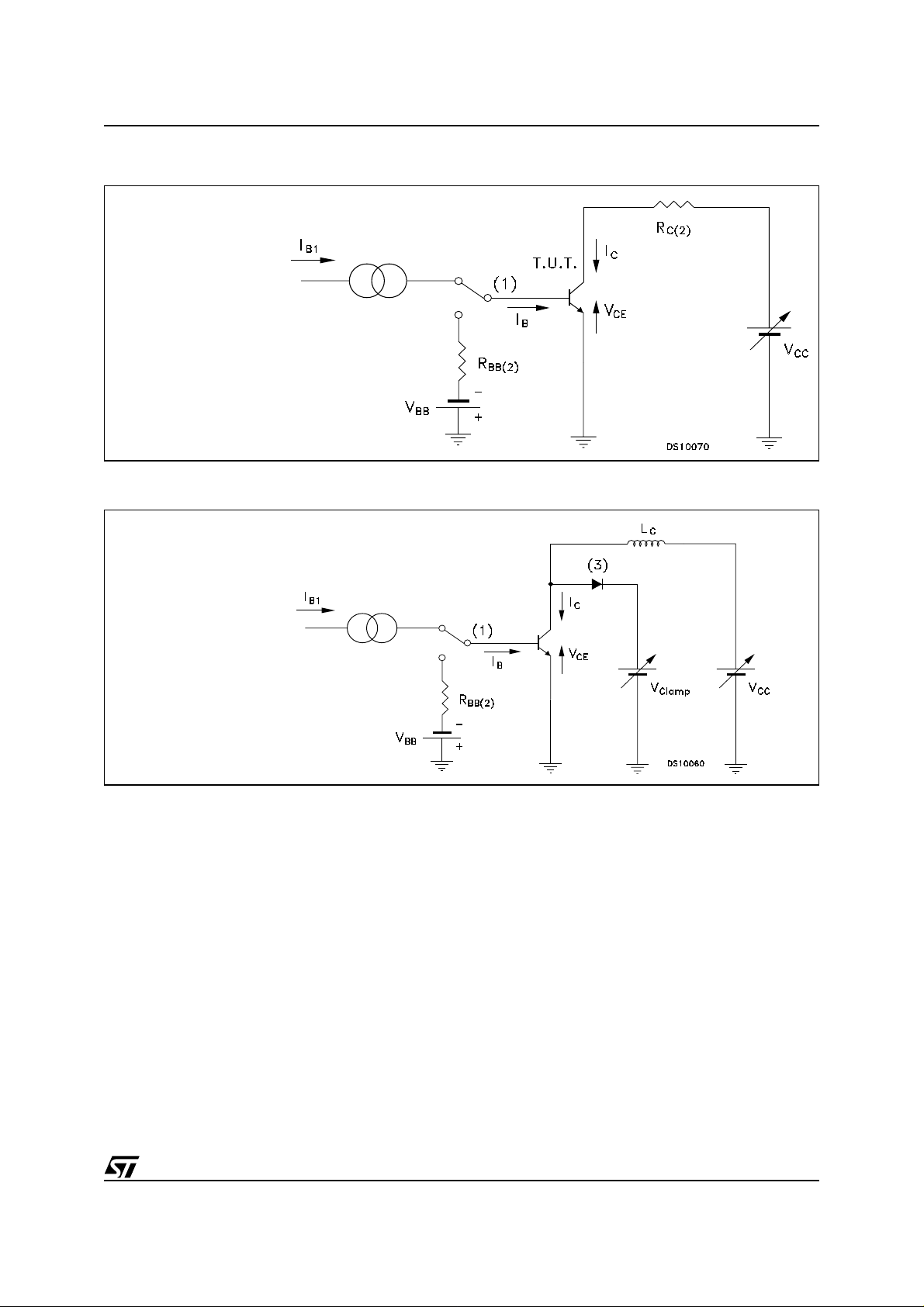
Figure 1: Resistive Load Switching Test Circuit
1) Fast Electronic Switch
2) Non-Inductive Resistor
Figure 2: Inductive Load Switching Tes t Circuit
STX13005 / STX13005- A P
1) Fast Electronic Switch
2) Non-Inductive Resistor
3) Fast Recovery Rectifier
5/8
Page 6

STX13005 / STX13005- AP
TO-92 BULK SHIPMENT MECHANICAL DATA
mm. inch
DIM.
MIN. TYP. MAX. MIN. TYP. MAX.
A 4.32 4.95 0.170 0.195
b 0.36 0.51 0.014 0.020
D 4.45 4.95 0.175 0.195
E 3.30 3.94 0.130 0.155
e 2.41 2.67 0.095 0.105
e1 1.14 1.40 0.045 0.055
L 12.70 15.49 0.500 0.610
R 2.16 2.41 0.085 0.095
S1 0.92 1.52 0.036 0.060
W 0.41 0.56 0.016 0.022
V5° 5°
6/8
Page 7

STX13005 / STX13005- A P
TO-92 AMMOPACK SHIPMENT (Suffix “-AP”) MECHANICAL DATA
DIM.
A1 4.80 0.189
T 3.80 0.150
T1 1.60 0.063
T2 2.30 0.091
d 0.48 0.019
P0 12.50 12.70 12.90 0.492 0.500 0.508
P2 5.65 6.35 7.05 0.222 0.250 0.278
F1, F2 2.44 2.54 2.94 0.096 0.100 0.116
delta H -2.00 2.00 -0.079 0.079
W 17.50 18.00 19.00 0.689 0.709 0.748
W0 5.70 6.00 6.30 0.224 0.236 0.248
W1 8.50 9.00 9.25 0.335 0.354 0.364
W2 0.50 0.020
H 18.50 20.50 0.728 0.807
H0 15.50 16.00 16.50 0.610 0.630 0.650
H1 25.00 0.984
D0 3.80 4.00 4.20 0.150 0.157 0.165
t 0.90 0.035
L 11.00 0.433
l1 3.00 0.118
delta P -1.00 1.00 -0.039 0.039
MIN. TYP. MAX. MIN. TYP. MAX.
mm. inch
7/8
Page 8

STX13005 / STX13005- AP
Information furnished is believed to be accurate and reliable. However, STMicroelectronics assumes no responsibility for t he
consequences of use of su ch in formation nor for any infri ngement of p atents or other rights of third parties w hich may result from
its use. No license is granted by implication or otherwise under any patent or patent rights of STMicroelectronics. Specifications
mentioned in this publication are subject to change without notice. This publication supersedes and replaces all information
previously suppli ed. STMi croelect ronics products are not author ized for use as c ritical component s in li fe suppo rt dev ices or
systems without express written approval of STMicroelectronics.
Australia - Brazil - Canada - China - Finland - France - Germany - Hong Kong - India - Israel - Italy - Japan - Malaysia - Malta - Morocco
© The ST logo is a registered trademark of STMicroelectronics
© 2002 STMicroelectronics - Printed in Italy - All Rights Reserved
Singapore - Spain - Sweden - Switzerland - United Kingdom - United States.
STMicroelectronics GROUP OF COMPANIES
© http://www.st.com
8/8
 Loading...