

Page 1
STW9NC80Z
N-CHANNEL 800V - 0.82Ω - 9.4A TO-247
Zener-Protected PowerMESH™III MOSFET
TYPE V
DSS
R
DS(on)
I
D
STW9NC80Z 800 V <0.9Ω 9.4 A
n
TYPICAL RDS(on) = 0.82Ω
n
EXTREMELY HIGH dv /d t C APABILITY
n
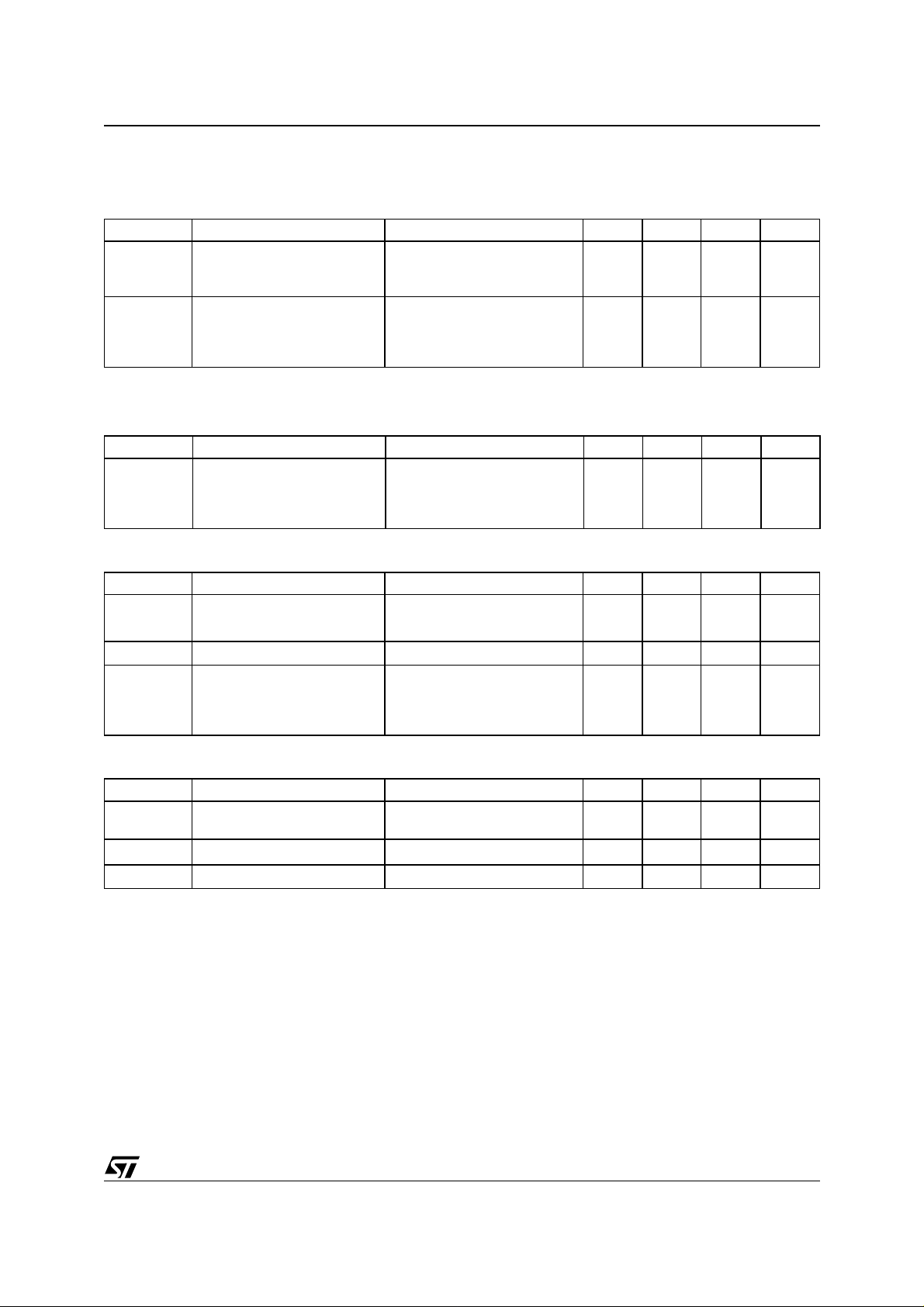
GATE-TO-SOURCE ZENER DIODES
n
100% AVALANCHE TESTED
n
VERY LOW INTRINSIC CAPAC ITANCES
n
GATE CHARGE MINIMIZED
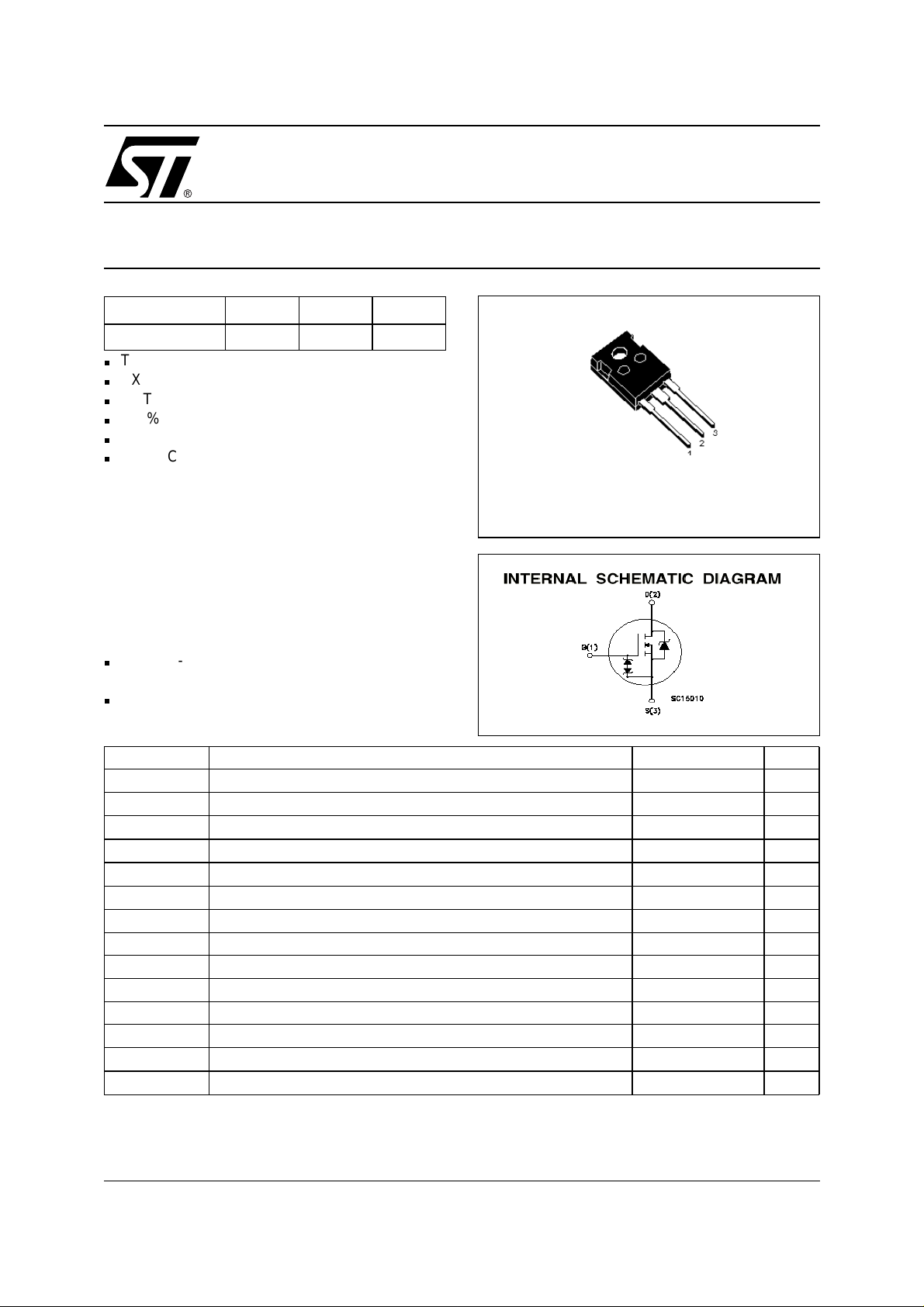
TO-247
DESCRIPTION
The third generation of MESH O VERLAY™ Power
MOSFETs for very high voltage exhibits unsurpassed on-resistance per unit area while integrating
back-to-back Zener diodes between gate and
source. Such arrangement gives extra ESD capability with higher ruggedness performance as requested by a large variety of single-switch applications.
APPLICATIONS
n
SINGLE-ENDED SMPS IN MONITORS,
COMPUTER AND INDUSTRIAL APPLICATION
n
WELDING EQUIPMENT
ABSOLUTE MAXIMUM RATINGS
Symbol Parameter Value Unit
V
DS
V
DGR
V
GS
I
D
I
D
I
(1)
DM
P
TOT
I
GS
V
ESD(G-S)
dv/dt(
V
ISO
T
stg
T
j
(•)Pu l se width limited by safe operating area
Drain-source Voltage (VGS = 0)
Drain-gate Voltage (RGS = 20 kΩ)
800 V
800 V
Gate- source Voltage ±25 V
Drain Current (continuous) at TC = 25°C
Drain Current (continuous) at TC = 100°C
9.4 A
5.9 A
Drain Current (pulsed) 38 A
Total Dissipation at TC = 25°C
190 W
Derating Factor 1.52 W/°C
Gate-source Current ±50 mA
Gate source ESD(HBM-C=100pF, R=15KΩ) 4KV
●) Peak Diode Recovery voltage slope 3 V/ns
Insulation Winthstand Voltage (DC) -- V
Storage Temperature –65 to 150 °C
Max. Operating Junction Temperature 150 °C
(1)ISD ≤9.4A, di/dt ≤100A/µs, VDD ≤ V
(BR)DSS
, Tj ≤ T
JMAX
1/8September 2002
Page 2

STW9NC80Z
THERMA L D ATA
Rthj-case Thermal Resistance Junction-case Max 0.66 °C/W
Rthj-amb Thermal Resistance Junction-ambient Max 30 °C/W
Rthc-sink Thermal Resistance Case-sink Typ 0.1 °C/W
T
AVALANCHE CHARACTERISTICS
Symbol Parameter Max Value Unit
I
AR
E
AS
Maximum Lead Temperature For Soldering Purpose 300 °C
l
Avalanche Current, Repetitive or Not-Repetitive
(pulse width limited by T
max)
j
Single Pulse Avalanche Energy
(starting T
= 25 °C, ID = IAR, VDD = 50 V)
j
9.4 A
350 mJ
ELECTRICAL CHARACTERISTICS (T
= 25 °C UNLESS OTHERWISE SPECIFIED)
CASE
OFF
Symbol Parameter Test Conditions Min. Typ. Max. Unit
V
(BR)DSS
Drain-source
ID = 250 µA, VGS = 0 800 V
Breakdown Voltage
∆BV
/∆TJBreakdown Voltage Temp.
DSS
ID = 1 mA, VGS = 0 1
Coefficient
V
= Max Rating
DS
VDS = Max Rating, TC = 125 °C
V
= ±20V
GS
1µA
50 µA
±10 µA
ON
I
I
(1)
DSS
GSS
Zero Gate Voltage
Drain Current (V
GS
Gate-body Leakage
Current (V
DS
= 0)
= 0)
Symbol Parameter Test Conditions Min. Typ. Max. Unit
V
V
GS(th)
R
DS(on)
Gate Threshold Voltage
Static Drain-source On
= VGS, ID = 250µA
DS
VGS = 10V, ID = 4.7A
345V
0.82 0.9 Ω
Resistance
I
D(on)
On State Drain Current VDS > I
V
GS
D(on)
=10V
x R
DS(on)max,
9.4 A
DYNAMIC
Symbol Parameter Test Conditions Min. Typ. Max. Unit
g
fs
C
iss
C
oss
C
rss
Forward Transconductance VDS > I
I
=4.7A
D
Input Capacitance
V
DS
Output Capacitance 230 pF
Reverse Transfer
Capacitance
D(on)
x R
DS(on)max,
= 25V, f = 1 MHz, VGS = 0
13 S
3500 pF
25 pF
V/°C
2/8
Page 3
STW9NC80Z
ELECTRICAL CHARACTERISTICS (CONTINUED)
SWITCHING ON (RESISTIVE LOAD)
Symbol Parameter Test Conditions Min. Typ. Max. Unit
V
t
d(on)
t
Q
Q
Q
r
gs
gd
Turn-on Delay Time
Rise Time 16 ns
Total Gate Charge
g
Gate-Source Charge 19.5 nC
Gate-Drain Charge 24.3 nC
SWITCHING OFF (INDUCTIVE LOAD)
Symbol Parameter Test Conditions Min. Typ. Max. Unit
t
r(Voff)
t
f
t
c
Off-voltage Rise Time
Fall Time 42 ns
Cross-over Time 67 ns
SOURCE DRAIN DIODE
Symbol Parameter Test Conditions Min. Typ. Max. Unit
I
SD
I
SDM
VSD (1)
t
rr
Q
rr
I
RRM
Source-drain Current 9.4 A
(2)
Source-drain Current (pulsed) 38 A
Forward On Voltage
Reverse Recovery Time
Reverse Recovery Charge 7.2 µC
Reverse Recovery Current 19.5 A
= 400V, ID = 4.5A
DD
RG= 4.7Ω VGS = 10V
(see test circuit, Figure 3)
V
= 640V, ID = 9 A,
DD
VGS = 10V
V
= 640V, ID = 9 A,
DD
RG=4.7Ω, V
GS
= 10V
(see test circuit, Figure 5)
ISD = 9 A, VGS = 0
I
= 9 A, di/dt = 100A/µs,
SD
VDD = 100V, Tj = 150°C
(see test circuit, Figure 5)
35 ns
72.2 101 nC
32 ns
1.6 V
730 ns
GATE-SOURCE ZENER DIODE
Symbol Parameter Test Conditions Min. Typ. Max. Unit
BV
GSO
Gate-Source Breakdown
Igs=± 1mA (Open Drain) 25 V
Voltage
αT Voltage Thermal Coefficient T=25°C Note(3) 1.3
I
Rz Dynamic Resistance
Note: 1. Pulsed: Pu l se duration = 300 µs, duty c ycle 1.5 %.
2. Pulse width li mited by safe operating area.
3. ∆V
= αT (25°-T ) BV
BV
GSO
(25°)
= 50 mA, VGS = 0
GS
90 Ω
10
-4
/°C
PROTECTION FEATURES OF GATE-TO-SOURCE ZENER DIODES
The built-in back-to-back Zener diodes have specif ically been designed to enhanc e not only t he dev ice’s
ESD capability, but also to make them safely absorb possible voltage transients that may occasionally be
applied from gate to source. In this respect the 25V Zener voltage is appropriate to achieve an efficient
and cost-effective intervention to protect the device’s integrity. These integrated Zener diodes thus avoid
the usage of external components.
3/8
Page 4

STW9NC80Z
Safe Operating Area For TO-247 Thermal Impedance For TO-247
Output Characteristics
Transfer Characteristics
Static Drain-source On ResistanceTransconductanc e
4/8
Page 5

Gate Charge vs Gate-source Voltage Capacitance Variations
Normalized On Resistance vs Temperatur eNormalized Gate Threshold Volta ge vs Temp.
STW9NC80Z
Source-drain Diode Forward Characteristics
5/8
Page 6

STW9NC80Z
Fig. 2: Unclamped Inductive WaveformFig. 1: Unclamped Inductive Load Test Circuit
Fig. 3: Switching Times Test Circuit For
Resistive Load
Fig. 5: Test Circuit For Inductive Load Switching
And Diode Recovery Times
Fig. 4: Gate Charge test Circuit
6/8
Page 7

TO-247 MECHANICAL DATA
STW9NC80Z
DIM.
MIN. TYP. MAX. MIN. TYP. MAX.
A 4.7 5.3 0.185 0.209
D 2.2 2.6 0.087 0.102
E 0.4 0.8 0.016 0.031
F 1 1.4 0.039 0.055
F3 2 2.4 0.079 0.094
F4 3 3.4 0.118 0.134
G 10.9 0.429
H 15.3 15.9 0.602 0.626
L 19.7 20.3 0.776 0.779
L3 14.2 14.8 0.559 0.582
L4 34.6 1.362
L5 5.5 0.217
M 2 3 0.079 0.118
mm inch
P025P
7/8
Page 8

STW9NC80Z
Information furnished is believed to be accurate and reliable. However, STMicroelectronics assumes no responsibility for the
consequences of use of su ch in formation nor for any in fringement of paten ts or o ther rights of third parties w hich may result from
its use. No license is granted by implication or otherwise under any patent or patent rights of STMicroelectronics. Specifications
mentioned in this publication are subject to change without notice. This publication supersedes and replaces all information
previously suppli ed. STMi croelect ronics pr oducts are not author ized for use as c ritical component s in li fe suppo rt devi ces or
systems without express written approval of STMicroelectronics.
Australia - Brazil - Canada - China - Finland - France - Germany - Hong Kong - India - Israel - Italy - Japan - Malaysia - Malta - Morocco
© The ST logo is a registered trademark of STMicroelectronics
© 2002 STMicroelectronics - Printed in Italy - All Rights Reserved
Singapore - Spain - Sweden - Switzerland - United Kingdom - United States.
STMicroelectronics GROUP OF COMPANIES
© http://www.st.com
8/8
 Loading...