

Page 1
STW9NA80
STH9NA80FI
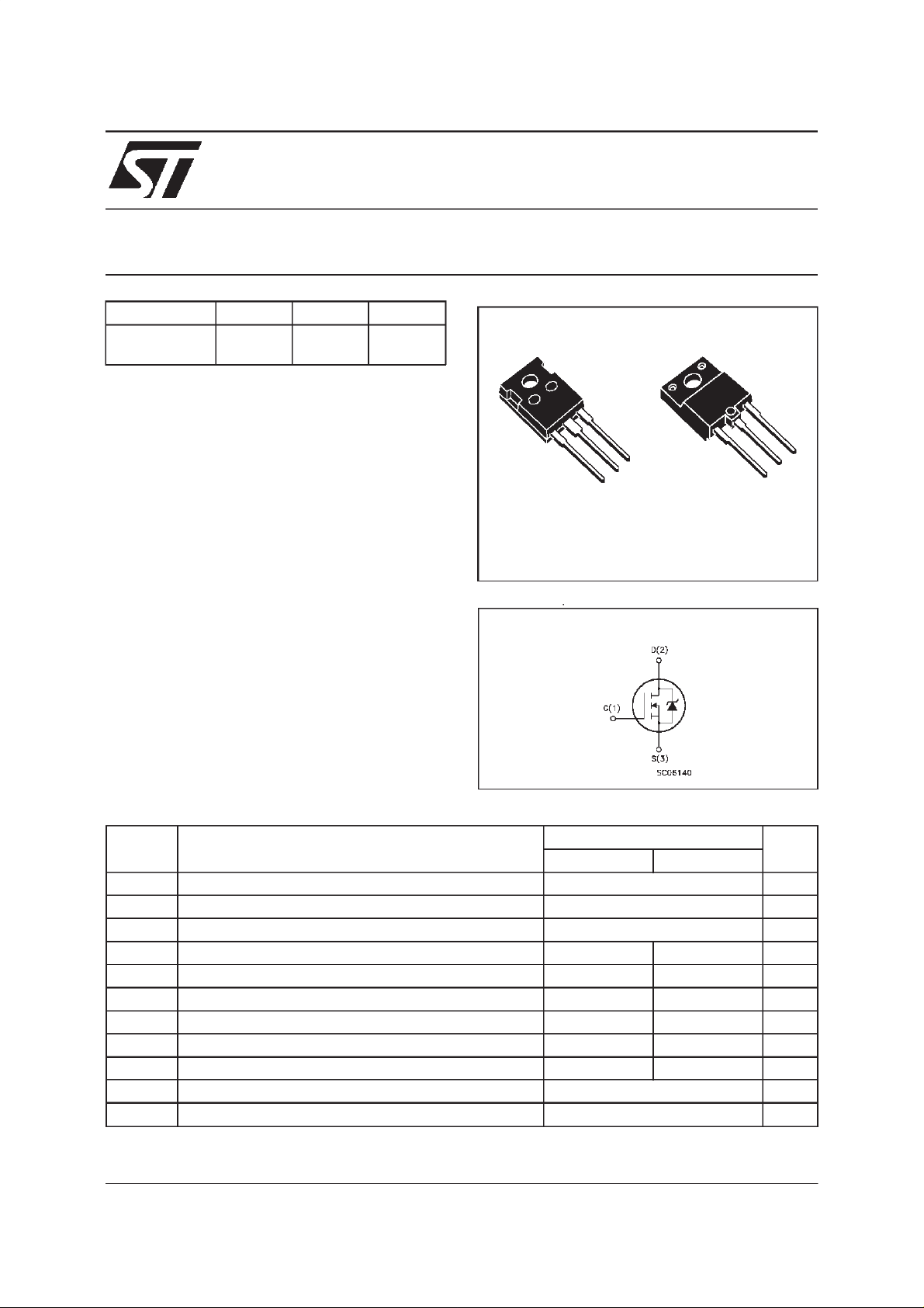
N - CHANNEL 800V - 0.85Ω - 9.1A - TO-247/ISOWATT218
FAST POWER MOS TRANSISTOR
TYPE V
STW9NA80
ST H9 NA80FI
■ TYPICALR
■ ± 30VGATETO SOURCEVOLTAGERATING
■ 100%AVALANCHETESTED
■ REPETITIVEAVALANCHEDATA AT 100
■ LOW INTRINSICCAPACITANCES
■ GATECHARGE MINIMIZED
■ REDUCEDTHRESHOLD VOLTAGESPREAD
DS(on)
DSS
800 V
800 V
= 0.85 Ω
APPLICATIONS
■ HIGHCURRENT, HIGH SPEED SWITCHING
■ SWITCHMODE POWER SUPPLIES(SMPS)
■ DC-AC CONVERTERS FOR WELDING
EQUIPMENTAND UNINTERRUPTIBLE
POWERSUPPLIESAND MOTORDRIVE
R
DS(on)
<1.0Ω
<1.0
Ω
I
D
9.1 A
5.9 A
o
C
3
2
1
3
2
1
TO-247 ISOWATT218
INTERNAL SCHEMATIC DIAGRAM
ABSOLUTE MAXIMUM RATINGS
Symbol Parameter Value Unit
ST W 9N A80 STH 9NA 80FI
V
V
V
I
DM
P
V
T
(•) Pulse width limited by safe operating area
November 1998
Drain-source Voltage (VGS=0) 800 V
DS
Dra in- gate Voltage (RGS=20kΩ)
DGR
Gate -sourc e Volta ge ± 30 V
GS
I
Drain C urrent (co ntinuous) at Tc=25oC9.15.9A
D
I
Drain C urrent (co ntinuous) at Tc=100oC63.9A
D
800 V
(•) Dra in Cur rent (pulsed) 36.4 36.4 A
Total Dissipation at Tc=25oC 190 80 W
tot
Der at in g Fac to r 1.52 0.64 W/
Insulat ion W ith stand Vo ltage (DC) 4000 V
ISO
St orage T empe r ature -65 t o 150
stg
T
Max. Op erating J unc t ion Tempe rat ure 150
j
o
o
o
C
C
C
1/10
Page 2
STW9NA80-STH9NA80FI
THERMAL DATA
TO-247 ISOWATT 218
R
thj-case
R
thj-amb
R
thc-sink
T
AVALANCHE CHARACTERISTICS
Symbol Para meter Max Val ue Uni t
I
AR
E
Ther mal Resistanc e Juncti on-case Max 0.65 1.56
Ther mal Resistanc e Juncti on-amb ien t Ma x
Thermal Resistance Case-sink Typ
Maximum Lead Temper at u r e Fo r Sold ering P urpose
l
Avalanche Cu rr ent, Repetitive or No t -Repet it iv e
(pulse width limited by T
Single Pulse Avalanche Energy
AS
(starting T
=25oC, ID=IAR,VDD=50V)
j
max)
j
30
0.1
300
9.1 A
415 mJ
o
C/W
o
C/W
o
C/W
o
C
ELECTRICAL CHARACTERISTICS
=25oC unless otherwisespecified)
(T
case
OFF
Symbol Parameter Test Condit ions Min. Typ. Max. Unit
V
(BR)DSS
Drain-sou rc e
=250µAVGS=0
I
D
800 V
Break d own V o lt age
I
DSS
I
GSS
Zero Gate Voltage
Drain Cu rr ent (V
GS
Gat e- b ody Le aka ge
Current (V
DS
=0)
=0)
V
=MaxRating
DS
= Max Rating Tc=100oC
V
DS
=± 30 V
V
GS
50
500
± 100 nA
ON(∗)
Symbol Parameter Test Condit ions Min. Typ. Max. Unit
V
GS(th)
Gate Threshold
V
DS=VGSID
= 250µA
2.25 3 3.75 V
Voltage
R
DS(on)
Static Drain-source On
VGS=10V ID= 4 .5 A 0.85 1 Ω
Resistance
I
D(on)
On S t ate D rain Cur rent VDS>I
D(on)xRDS(on)max
9.1 A
VGS=10V
DYNAMIC
Symbol Parameter Test Condit ions Min. Typ. Max. Unit
g
(∗)Forward
fs
Tr anscond uctance
C
C
C
Input Cap ac i t an c e
iss
Out put Capacita nc e
oss
Reverse Transf er
rss
Capacitance
VDS>I
D(on)xRDS(on)maxID
=4.5A 7.5 10 S
VDS=25V f=1MHz VGS= 0 2900
290
80
3800
380
105
µ
µA
pF
pF
pF
A
2/10
Page 3
STW9NA80-STH9NA80FI
ELECTRICAL CHARACTERISTICS
(continued)
SWITCHING ON
Symbol Parameter Test Condit ions Min. Typ. Max. Unit
t
d(on)
Turn-on Time
t
r
Rise Time
VDD= 400 V ID=4.5A
=4.7 Ω VGS=10V
R
G
37
45
50
60
(see test circuit, figure 3)
Q
Q
Q
Total Gate Charge
g
Gat e- Sour ce Char ge
gs
Gate-Drain Charge
gd
VDD= 640 V ID=9A VGS=10V 115
15
55
150 nC
SWITCHING OFF
Symbol Parameter Test Condit ions Min. Typ. Max. Unit
t
r(Voff)
t
t
Off -voltage Rise Time
Fall Time
f
Cross-over Ti me
c
VDD= 640 V ID=9A
=4.7 Ω VGS=10V
R
G
(see test circuit, figure 5)
45
15
70
60
20
91
SOURCEDRAINDIODE
Symbol Parameter Test Condit ions Min. Typ. Max. Unit
I
SD
I
SDM
V
SD
t
Q
I
RRM
(∗) Pulsed: Pulse duration = 300 µs, duty cycle 1.5 %
(•) Pulse width limited by safe operating area
Source-drain Curr ent
(•)
Source-drain Curr ent
9.1
36.4
(pulsed)
(∗) For ward O n Voltage ISD=9.1A VGS=0 1.6 V
Reverse Reco v ery
rr
Time
Reverse Reco v ery
rr
= 9 A di/dt = 100 A/µs
I
SD
= 100 V Tj=150oC
V
DD
(see test circuit, figure 5)
765
113.4
Charge
Reverse Reco v ery
35
Current
ns
ns
nC
nC
ns
ns
ns
A
A
ns
µ
A
C
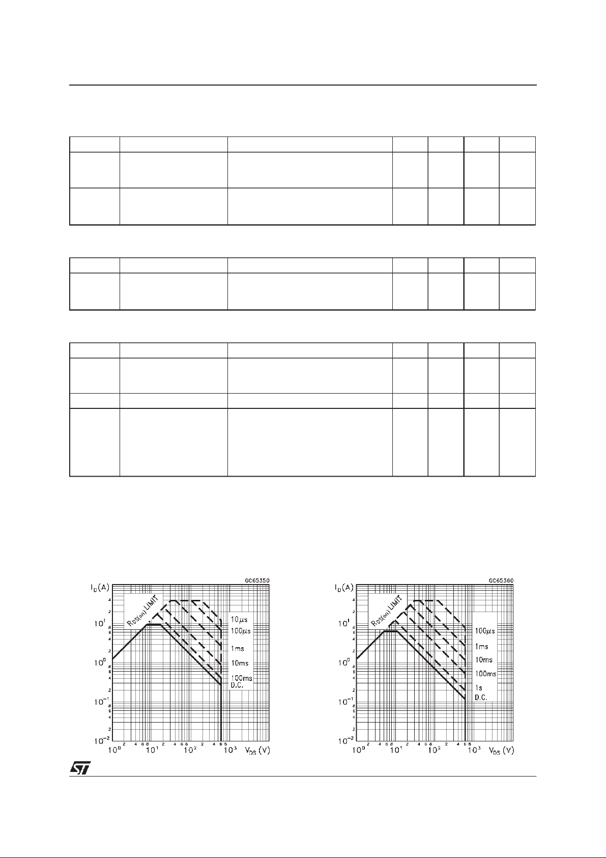
SafeOperating Area for TO-247 SafeOperating Area for ISOWATT218
3/10
Page 4

STW9NA80-STH9NA80FI
ThermalImpedancefor TO-247
DeratingCurve for TO-247
ThermalImpedancefor ISOWATT218
DeratingCurve for ISOWATT218
OutputCharacteristics
4/10
TransferCharacteristics
Page 5

STW9NA80-STH9NA80FI
Transconductance
Gate Charge vs Gate-sourceVoltage
Static Drain-sourceOn Resistance
CapacitanceVariations
Normalized Gate Threshold Voltage vs
Temperature
Normalized On Resistancevs Temperature
5/10
Page 6

STW9NA80-STH9NA80FI
Turn-onCurrentSlope
Cross-overTime
Turn-offDrain-sourceVoltageSlope
SwitchingSafe Operating Area
AccidentalOverloadArea
6/10
Source-drainDiode Forward Characteristics
Page 7

STW9NA80-STH9NA80FI
Fig. 1:
UnclampedInductiveLoad TestCircuit
Fig. 3: Switching Times Test CircuitsFor
ResistiveLoad
Fig. 2:
UnclampedInductive Waveform
Fig. 4: Gate Charge test Circuit
Fig. 5:
Test CircuitFor InductiveLoad Switching
And Diode Recovery Times
7/10
Page 8

STW9NA80-STH9NA80FI
TO-247 MECHANICAL DATA
DIM.
MIN. TYP. MAX. MIN. TYP. MAX.
A 4.7 5.3 0.185 0.209
D 2.2 2.6 0.087 0.102
E 0.4 0.8 0.016 0.031
F 1 1.4 0.039 0.055
F3 2 2.4 0.079 0.094
F4 3 3.4 0.118 0.134
G 10.9 0.429
H 15.3 15.9 0.602 0.626
L 19.7 20.3 0.776 0.779
L3 14.2 14.8 0 .559 0.413 0.582
L4 34.6 1.362
L5 5.5 0.217
M 2 3 0.079 0.118
Dia 3.55 3.65 0.140 0.144
mm inch
8/10
P025P
Page 9

ISOWATT218MECHANICAL DATA
STW9NA80-STH9NA80FI
DIM.
mm inch
MIN. TYP. MAX. MIN. TYP. MAX.
A 5.35 5.65 0.210 0.222
C 3.3 3.8 0.130 0.149
D 2.9 3.1 0.114 0.122
D1 1.88 2.08 0.074 0.081
E 0.75 1 0.029 0.039
F 1.05 1.25 0.041 0.049
G 10.8 11.2 0.425 0.441
H 15.8 16.2 0.622 0.637
L1 20.8 21.2 0.818 0.834
L2 19.1 19.9 0.752 0.783
L3 22.8 23.6 0.897 0.929
L4 40.5 42.5 1.594 1.673
L5 4.85 5.25 0.190 0.206
L6 20.25 20.75 0.797 0.817
M 3.5 3.7 0.137 0.145
N 2.1 2.3 0.082 0.090
U 4.6 0.181
L3
N
E
A
D
C
L5
M
H
L2
L6
L1
D1
F
U
G
123
L4
P025C
9/10
Page 10

STW9NA80-STH9NA80FI
Information furnished is believed to beaccurate and reliable. However, STMicroelectronics assumes no responsibility forthe consequences
of use of such information nor for any infringement of patents or other rights of third parties which may result from its use. No license is
granted by implication or otherwise under any patent or patent rights of STMicroelectronics. Specification mentioned in this publication are
subject to change without notice. This publication supersedes and replaces all information previously supplied. STMicroelectronics products
are not authorized for use as critical components in life support devices or systems without express written approval of STMicroelectronics.
The ST logo is a registered trademarkof STMicroelectronics
1998 STMicroelectronics – Printed in Italy – All Rights Reserved
STMicroelectronics GROUP OF COMPANIES
Australia - Brazil - Canada - China -France - Germany - Italy - Japan - Korea - Malaysia - Malta - Mexico -Morocco - The Netherlands -
Singapore - Spain - Sweden - Switzerland - Taiwan - Thailand - UnitedKingdom - U.S.A.
http://www.st.com
.
10/10
 Loading...