

Page 1
STW9NA60
N - CHANNEL ENHANCEMENT MODE
FAST POWER MOS TRANSISTOR
TYPE V
STW9NA60
ST H9NA60FI
■ TYPICALR
■ ± 30V GATE TO SOURCE VOLTAGERATING
■ 100%AVALANCHETESTED
■ REPETITIVEAVALANCHEDATA AT 100
■ LOW INTRINSICCAPACITANCES
■ GATECHARGE MINIMIZED
■ REDUCEDTHRESHOLD VOLTAGE SPREAD
DS(on)
DSS
600 V
600 V
= 0.69 Ω
APPLICATIONS
■ HIGHCURRENT, HIGH SPEEDSWITCHING
■ SWITCHMODE POWER SUPPLIES (SMPS)
■ DC-AC CONVERTERS FOR WELDING
EQUIPMENTANDUNINTERRUPTIBLE
POWERSUPPLIESAND MOTORDRIVE
R
DS(on)
<0.8Ω
<0.8Ω
I
D
9.5 A
6.4 A
o
C
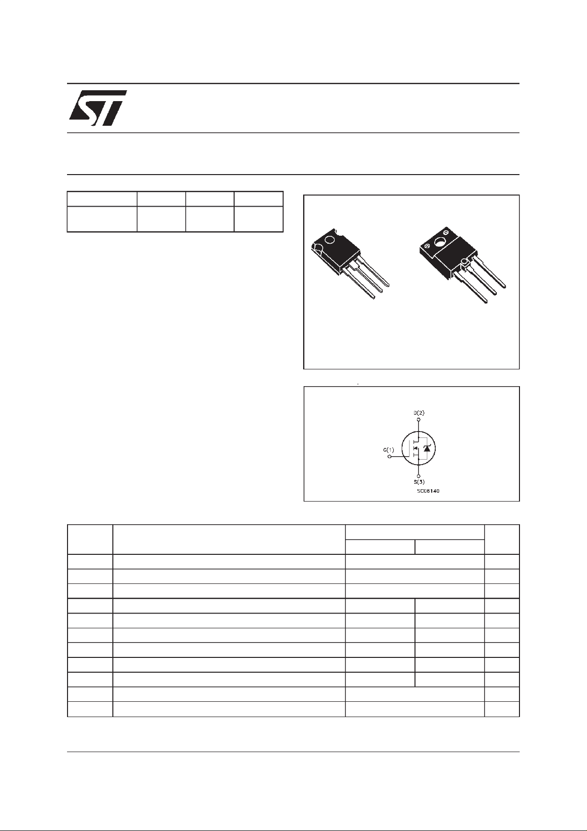
STH9NA60FI
3
2
1
TO-247 ISOWATT218
INTERNAL SCHEMATIC DIAGRAM
1
3
2
ABSOLUTE MAXIMUM RATINGS
Symbol Parameter Value Unit
STW9NA60 ST H9NA 60FI
V
V
V
I
DM
P
V
T
(•) Pulse width limited by safe operating area
October 1998
Dra in- sour c e Volt age (VGS= 0) 600 V
DS
Dra in- gat e Voltage (RGS=20kΩ) 600 V
DGR
Gat e-source Volt age
GS
I
Dra in Cu rr ent (contin uous ) a t Tc=25oC6.49.5A
D
I
Dra in Cu rr ent (contin uous ) a t Tc=100oC46A
D
30 V
±
(•) Dra in Cu rr ent (pulsed) 38 38 A
Tot al Dissipation at Tc=25oC70160W
tot
Der ati ng Fact or 0.56 1.28 W/
Insulation Withstand Voltage (DC) 4000 V
ISO
St orage Temperat ure -65 to 150
stg
T
Max. Operating Junct ion Temperat ure 150
j
o
o
o
C
C
C
1/10
Page 2
STW9NA60-STH9NA60FI
THERMAL DATA
TO-247 ISOWATT218
R
thj-case
R
thj-amb
R
thc-sink
T
AVALANCHE CHARACTERISTICS
Symbol Parameter Max V alue Unit
I
AR
E
Ther mal Resistanc e Junct ion-case Max 0.78 1.78
Ther mal Resistanc e Junct ion-ambient Max
Ther mal Resistanc e Case-sink Ty p
Maximum Lead T e m pe ra t ure F or S o ldering Purpos e
l
Avalanche C urrent, R epetitive or Not-Repetitive
(pulse width limited by T
Single Pul se Avalanc he Ener gy
AS
(starting T
=25oC, ID=IAR,VDD=50V)
j
max,δ <1%)
j
30
0.1
300
9.5 A
450 mJ
o
C/W
o
C/W
o
C/W
o
C
ELECTRICAL CHARACTERISTICS
=25oC unless otherwisespecified)
(T
case
OFF
Symbol Parameter Test Conditions Min. Typ. Max. Unit
V
(BR)DSS
Drain-source
ID=250µAVGS= 0 600 V
Break dow n Vo lt age
I
DSS
I
GSS
Zero Gate Voltage
Drain Curre nt (V
GS
Gat e- bod y Leakag e
Current (V
DS
=0)
=0)
V
=MaxRating
DS
=MaxRating Tc= 100oC
V
DS
V
=± 30 V
GS
25
250
100 nA
±
ON(∗)
Symbol Parameter Test Conditions Min. Typ. Max. Unit
V
GS(th)
R
DS(on)
Gate Threshold Voltage VDS=VGSID= 250µA2.2533.75V
Sta t ic Drain-s our c e On
VGS=10V ID= 4.5A 0.69 0.8
Resistance
I
D(on)
On State Drain Current VDS>I
D(on)xRDS(on)max
9A
VGS=10V
DYNAMIC
Symbol Parameter Test Conditions Min. Typ. Max. Unit
g
(∗)Forward
fs
Tr ansc on duc tance
C
C
C
Input Capaci t ance
iss
Out put Capac itance
oss
Reverse Transfer
rss
Capacit a nc e
VDS>I
D(on)xRDS(on)maxID
=4.5A 5 8.3 S
VDS=25V f=1MHz VGS= 0 1800
230
65
2350
300
85
µA
µA
Ω
pF
pF
pF
2/10
Page 3
STW9NA60-STH9NA60FI
ELECTRICAL CHARACTERISTICS
(continued)
SWITCHINGON
Symbol Parameter Test Conditions Min. Typ. Max. Unit
t
d(on)
t
r
Turn-on Time
Rise Time
VDD=300V ID= 4.5 A
R
=4.7
G
Ω
VGS=10V
21
32
30
45
(see test circuit, figure 3)
(di/dt)
Tur n-on Current Slope VDD=480V ID=9A
on
R
G
=47
Ω
VGS=10V
180 A/ µ s
(see test circuit, figure 5)
Q
Q
Q
Tot al Gate Charge
g
Gat e- Source Charge
gs
Gate-Drain Charge
gd
VDD= 480 V ID=9A VGS=10V 75
11
36
100 nC
SWITCHINGOFF
Symbol Parameter Test Conditions Min. Typ. Max. Unit
t
r(Voff)
t
t
Off-voltage Rise Tim e
Fall T ime
f
Cross-over Tim e
c
VDD=480V ID=9A
=4.7 Ω VGS=10V
R
G
(see test circuit, figure 5)
16
18
26
23
25
35
SOURCEDRAINDIODE
Symbol Parameter Test Conditions Min. Typ. Max. Unit
I
SD
I
SDM
V
SD
t
Q
I
RRM
(∗) Pulsed:Pulse duration = 300 µs, duty cycle 1.5 %
(•) Pulse width limited by safe operatingarea
Source-drain Current
(•)
Source-drain Current
9.5
38
(pulsed)
(∗)ForwardOnVoltage ISD=9.5A VGS=0 1.6 V
Reverse Recovery
rr
Time
Reverse Recovery
rr
ISD= 9. 5 A di/dt = 100 A/µs
= 100 V Tj=150oC
V
DD
(see test circuit, figure 5)
660
12
Charge
Reverse Recovery
36
Current
ns
ns
nC
nC
ns
ns
ns
A
A
ns
µC
A
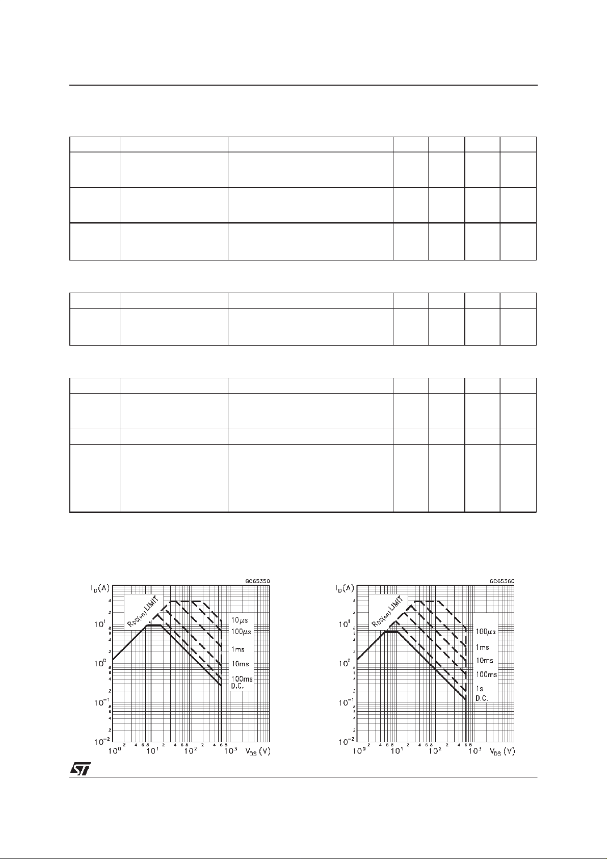
SafeOperating Area for TO-247 SafeOperating Area for ISOWATT218
3/10
Page 4

STW9NA60-STH9NA60FI
ThermalImpedancefor TO-247
DeratingCurve for TO-247
ThermalImpedancefor ISOWATT218
DeratingCurve for ISOWATT218
OutputCharacteristics
4/10
TransferCharacteristics
Page 5

STW9NA60-STH9NA60FI
Transconductance
Gate Charge vs Gate-sourceVoltage
Static Drain-sourceOn Resistance
CapacitanceVariations
NormalizedGate ThresholdVoltage vs
Temperature
NormalizedOn Resistancevs Temperature
5/10
Page 6

STW9NA60-STH9NA60FI
Turn-onCurrentSlope
Cross-overTime
Turn-offDrain-sourceVoltage Slope
SwitchingSafe Operating Area
AccidentalOverload Area
6/10
Source-drainDiode ForwardCharacteristics
Page 7

STW9NA60-STH9NA60FI
Fig. 1:
UnclampedInductiveLoad TestCircuit
Fig. 3: SwitchingTimes TestCircuits For
ResistiveLoad
Fig. 2:
UnclampedInductive Waveform
Fig. 4: Gate Chargetest Circuit
Fig. 5:
Test Circuit For InductiveLoad Switching
And Diode Recovery Times
7/10
Page 8

STW9NA60-STH9NA60FI
TO-247 MECHANICAL DATA
DIM.
MIN. TYP. MAX. MIN. TYP. MAX.
A 4.7 5.3 0.185 0.209
D 2.2 2.6 0.087 0.102
E 0.4 0.8 0.016 0.031
F 1 1.4 0.039 0.055
F3 2 2.4 0.079 0.094
F4 3 3.4 0.118 0.134
G 10.9 0.429
H 15.3 15.9 0.602 0.626
L 19.7 20.3 0.776 0.779
L3 14.2 14.8 0.559 0.413 0.582
L4 34.6 1.362
L5 5.5 0.217
M 2 3 0.079 0.118
Dia 3.55 3.65 0.140 0.144
mm inch
8/10
P025P
Page 9

ISOWATT218MECHANICAL DATA
STW9NA60-STH9NA60FI
DIM.
mm inch
MIN. TYP. MAX. MIN. TYP. MAX.
A 5.35 5.65 0.210 0.222
C 3.3 3.8 0.130 0.149
D 2.9 3.1 0.114 0.122
D1 1.88 2.08 0.074 0.081
E 0.75 1 0.029 0.039
F 1.05 1.25 0.041 0.049
G 10.8 11.2 0.425 0.441
H 15.8 16.2 0.622 0.637
L1 20.8 21.2 0.818 0.834
L2 19.1 19.9 0.752 0.783
L3 22.8 23.6 0.897 0.929
L4 40.5 42.5 1.594 1.673
L5 4.85 5.25 0.190 0.206
L6 20.25 20.75 0.797 0.817
M 3.5 3.7 0.137 0.145
N 2.1 2.3 0.082 0.090
U 4.6 0.181
L3
N
E
A
D
C
L5
M
H
L2
L6
L1
D1
F
U
G
123
L4
P025C
9/10
Page 10

STW9NA60-STH9NA60FI
Information furnished is believed to be accurate and reliable. However, STMicroelectronics assumes no responsibility for the consequences
of use of such information nor for any infringement of patents or other rights of third parties which may result from its use. No license is
granted by implicationor otherwise under any patent or patent rights of STMicroelectronics. Specification mentioned in thispublication are
subject to change without notice. This publication supersedes and replaces all information previously supplied. STMicroelectronics products
are not authorized for use as critical components in life support devices or systems without express written approval of STMicroelectronics.
The ST logo is a trademarkof STMicroelectronics
1998 STMicroelectronics – Printed in Italy –All Rights Reserved
STMicroelectronics GROUP OF COMPANIES
Australia - Brazil - Canada -China -France -Germany - Italy - Japan - Korea - Malaysia -Malta - Mexico - Morocco -The Netherlands -
Singapore - Spain - Sweden - Switzerland - Taiwan - Thailand - United Kingdom - U.S.A.
http://www.st.com
.
10/10
 Loading...