

Page 1
RF down converter with embedded integer-N synthesizer
Features
■ High linearity:
– IIP3: +24.5 dBm
– 2FRF-2FLO spurious rejection: 75 dBc
■ Noise figure:
–NF: 9.5dB
■ Conversion gain
– CG: 8.5 dB
■ RF range: 695 MHz to 960 MHz
■ Wide IF amplifier frequency range: 70 MHz to
400 MHz
■ Integrated RF balun with internal matching
■ Dual differential integrated VCOs with
automatic center frequency calibration:
– LOA: 850 to 1025 MHz
– LOB: 1025 to 1185 MHz
■ Embedded integer-N synthesizer
– Dual modulus programmable prescaler
(16/17 or 19/20)
– Programmable reference frequency divider
(10 bits)
– Adjustable charge pump current
– Digital lock detector
– Excellent integrated phase noise
– Fast lock time: 150 µs
■ Integrated DAC with dual current output
■ Supply: 3.3 V and 5 V analog,
3.3 V digital
■ Dual digital bus interface: SPI and I
mode) with 3 bit programmable address
(1101A
■ Process: 0.35 µm BICMOS SiGe
■ Operating temperature range -40 to +85
■ 44-lead exposed pad VFQFPN
2A1A0
)
package 7x7x1.0 mm
2
C bus (fast
o
C
STW82101B
Datasheet − production data
VFQFPN-44
Applications
■ Cellular infrastructure equipment:
– IF sampling receivers
– Digital PA linearization loops
■ Other wireless communication systems.
Table 1. Device summary
Part number Package Packaging
STW82101B VFQFPN-44 Tray
STW82101BTR VFQFPN-44 Tape and reel
Description
The STMicroelectronics STW82101B is an
integrated down converter providing 8.5 dB of
gain, 9.5 dB NF, and a very high input linearity by
means of its passive mixer.
Embedding two wide band auto calibrating VCOs
and an integer-N synthesizer, the STW82101B is
suitable for both Rx and Tx requirements for
Cellular infrastructure equipment.
The integrated RF balun and internal matching
permit direct 50 ohm single-ended interface to RF
port. The IF output is suitable for driving 200-ohm
impedance filters.
By embedding a DAC with dual current output to
drive an external PIN diode attenuator, the
STW82101B replaces several costly discrete
components and offers a significant footprint
reduction.
The STW82101B device is designed with
STMicroelectronics advanced 0.35 µm
SiGe process. Its performance is specified over a
-40 °C to +85 °C temperature range.
May 2012 Doc ID 018503 Rev 3 1/68
This is information on a product in full production.
www.st.com
1
Page 2

Contents STW82101B
Contents
1 Block diagram . . . . . . . . . . . . . . . . . . . . . . . . . . . . . . . . . . . . . . . . . . . . . . 7
2 Pin description . . . . . . . . . . . . . . . . . . . . . . . . . . . . . . . . . . . . . . . . . . . . . 8
3 Absolute maximum ratings . . . . . . . . . . . . . . . . . . . . . . . . . . . . . . . . . . 11
4 Operating conditions . . . . . . . . . . . . . . . . . . . . . . . . . . . . . . . . . . . . . . . 12
5 Test conditions . . . . . . . . . . . . . . . . . . . . . . . . . . . . . . . . . . . . . . . . . . . . 14
6 Electrical characteristics . . . . . . . . . . . . . . . . . . . . . . . . . . . . . . . . . . . . 15
7 Typical performance characteristics . . . . . . . . . . . . . . . . . . . . . . . . . . . 21
8 General description . . . . . . . . . . . . . . . . . . . . . . . . . . . . . . . . . . . . . . . . . 24
8.1 Circuit description . . . . . . . . . . . . . . . . . . . . . . . . . . . . . . . . . . . . . . . . . . . 24
8.1.1 Reference input stage . . . . . . . . . . . . . . . . . . . . . . . . . . . . . . . . . . . . . . 24
8.1.2 Reference divider . . . . . . . . . . . . . . . . . . . . . . . . . . . . . . . . . . . . . . . . . . 25
8.1.3 Prescaler . . . . . . . . . . . . . . . . . . . . . . . . . . . . . . . . . . . . . . . . . . . . . . . . 25
8.1.4 A and B counters . . . . . . . . . . . . . . . . . . . . . . . . . . . . . . . . . . . . . . . . . . 25
8.1.5 Phase frequency detector (PFD) . . . . . . . . . . . . . . . . . . . . . . . . . . . . . . 26
8.1.6 Lock detect . . . . . . . . . . . . . . . . . . . . . . . . . . . . . . . . . . . . . . . . . . . . . . 27
8.1.7 Mute until lock . . . . . . . . . . . . . . . . . . . . . . . . . . . . . . . . . . . . . . . . . . . . 27
8.1.8 Charge pump . . . . . . . . . . . . . . . . . . . . . . . . . . . . . . . . . . . . . . . . . . . . . 27
8.1.9 Voltage controlled oscillators . . . . . . . . . . . . . . . . . . . . . . . . . . . . . . . . . 28
VCO selection. . . . . . . . . . . . . . . . . . . . . . . . . . . . . . . . . . . . . . . . . . . . . . . . . . . .28
VCO frequency calibration . . . . . . . . . . . . . . . . . . . . . . . . . . . . . . . . . . . . . . . . . .28
VCO calibration auto-restart feature. . . . . . . . . . . . . . . . . . . . . . . . . . . . . . . . . . .30
VCO voltage amplitude control. . . . . . . . . . . . . . . . . . . . . . . . . . . . . . . . . . . . . . .30
8.1.10 Output stage . . . . . . . . . . . . . . . . . . . . . . . . . . . . . . . . . . . . . . . . . . . . . 31
8.1.11 External VCO buffer . . . . . . . . . . . . . . . . . . . . . . . . . . . . . . . . . . . . . . . . 31
8.1.12 Mixer and IF amplifier . . . . . . . . . . . . . . . . . . . . . . . . . . . . . . . . . . . . . . 32
LO mixer driver . . . . . . . . . . . . . . . . . . . . . . . . . . . . . . . . . . . . . . . . . . . . . . . . . . .32
Mixer. . . . . . . . . . . . . . . . . . . . . . . . . . . . . . . . . . . . . . . . . . . . . . . . . . . . . . . . . . .32
IF amplifier . . . . . . . . . . . . . . . . . . . . . . . . . . . . . . . . . . . . . . . . . . . . . . . . . . . . . .33
8.1.13 Dual output current DAC . . . . . . . . . . . . . . . . . . . . . . . . . . . . . . . . . . . . 33
2/68 Doc ID 018503 Rev 3
Page 3

STW82101B Contents
9 I2C bus interface . . . . . . . . . . . . . . . . . . . . . . . . . . . . . . . . . . . . . . . . . . . 34
9.1 I2C general features . . . . . . . . . . . . . . . . . . . . . . . . . . . . . . . . . . . . . . . . . 34
9.1.1 Data validity . . . . . . . . . . . . . . . . . . . . . . . . . . . . . . . . . . . . . . . . . . . . . . 34
9.1.2 START and STOP conditions . . . . . . . . . . . . . . . . . . . . . . . . . . . . . . . . . 35
START condition . . . . . . . . . . . . . . . . . . . . . . . . . . . . . . . . . . . . . . . . . . . . . . . . .35
STOP condition . . . . . . . . . . . . . . . . . . . . . . . . . . . . . . . . . . . . . . . . . . . . . . . . . .35
9.1.3 Byte format and acknowledge . . . . . . . . . . . . . . . . . . . . . . . . . . . . . . . . 35
9.1.4 Device addressing . . . . . . . . . . . . . . . . . . . . . . . . . . . . . . . . . . . . . . . . . 36
9.1.5 Single-byte write mode . . . . . . . . . . . . . . . . . . . . . . . . . . . . . . . . . . . . . 36
9.1.6 Multi-byte write mode . . . . . . . . . . . . . . . . . . . . . . . . . . . . . . . . . . . . . . . 36
9.1.7 Current byte address read . . . . . . . . . . . . . . . . . . . . . . . . . . . . . . . . . . . 36
9.2 I2C timing specifications . . . . . . . . . . . . . . . . . . . . . . . . . . . . . . . . . . . . . . 37
9.2.1 Data and clock timing specification . . . . . . . . . . . . . . . . . . . . . . . . . . . . 37
9.2.2 I
9.2.3 I
2
C START and STOP timing specification . . . . . . . . . . . . . . . . . . . . . . 37
2
C acknowledge timing specification . . . . . . . . . . . . . . . . . . . . . . . . . . 38
9.3 I2C registers . . . . . . . . . . . . . . . . . . . . . . . . . . . . . . . . . . . . . . . . . . . . . . . 39
9.3.1 I2C register summary . . . . . . . . . . . . . . . . . . . . . . . . . . . . . . . . . . . . . . . 39
9.3.2 I
2
C register definitions . . . . . . . . . . . . . . . . . . . . . . . . . . . . . . . . . . . . . . 40
9.4 Device calibration through the I2C interface . . . . . . . . . . . . . . . . . . . . . . . 46
9.4.1 VCO calibration procedure (I2C interface) . . . . . . . . . . . . . . . . . . . . . . . 46
9.4.2 Power ON sequence (I
9.4.3 VCO calibration auto-restart procedure (I
2
C interface) . . . . . . . . . . . . . . . . . . . . . . . . . . . . 46
2
C interface) . . . . . . . . . . . . . 47
10 SPI digital interface . . . . . . . . . . . . . . . . . . . . . . . . . . . . . . . . . . . . . . . . . 48
10.1 SPI general features . . . . . . . . . . . . . . . . . . . . . . . . . . . . . . . . . . . . . . . . . 48
10.2 SPI timing specification . . . . . . . . . . . . . . . . . . . . . . . . . . . . . . . . . . . . . . 50
10.2.1 Data, clock and load timing . . . . . . . . . . . . . . . . . . . . . . . . . . . . . . . . . . 50
10.3 SPI registers . . . . . . . . . . . . . . . . . . . . . . . . . . . . . . . . . . . . . . . . . . . . . . . 51
10.3.1 SPI register summary . . . . . . . . . . . . . . . . . . . . . . . . . . . . . . . . . . . . . . 51
10.3.2 SPI register definitions . . . . . . . . . . . . . . . . . . . . . . . . . . . . . . . . . . . . . . 51
10.4 Device calibration through the SPI interface . . . . . . . . . . . . . . . . . . . . . . 54
10.4.1 VCO calibration procedure (SPI interface) . . . . . . . . . . . . . . . . . . . . . . . 54
10.4.2 Power ON sequence (SPI interface) . . . . . . . . . . . . . . . . . . . . . . . . . . . 54
10.4.3 VCO calibration auto-restart procedure (SPI interface) . . . . . . . . . . . . . 55
Doc ID 018503 Rev 3 3/68
Page 4

Contents STW82101B
11 Application information . . . . . . . . . . . . . . . . . . . . . . . . . . . . . . . . . . . . . 56
11.1 Application circuit . . . . . . . . . . . . . . . . . . . . . . . . . . . . . . . . . . . . . . . . . . . 56
11.2 Standard Mode Operation . . . . . . . . . . . . . . . . . . . . . . . . . . . . . . . . . . . . 58
11.3 Diversity mode operation with same LO frequency . . . . . . . . . . . . . . . . . 59
11.4 Diversity mode operation with different LO frequencies . . . . . . . . . . . . . . 60
11.5 External VCO standard mode operation . . . . . . . . . . . . . . . . . . . . . . . . . 61
11.6 External VCO diversity mode operation with same LO . . . . . . . . . . . . . . 62
12 Evaluation kit . . . . . . . . . . . . . . . . . . . . . . . . . . . . . . . . . . . . . . . . . . . . . . 63
13 Package mechanical data . . . . . . . . . . . . . . . . . . . . . . . . . . . . . . . . . . . . 64
14 Revision history . . . . . . . . . . . . . . . . . . . . . . . . . . . . . . . . . . . . . . . . . . . 66
4/68 Doc ID 018503 Rev 3
Page 5

STW82101B List of tables
List of tables
Table 1. Device summary . . . . . . . . . . . . . . . . . . . . . . . . . . . . . . . . . . . . . . . . . . . . . . . . . . . . . . . . . . 1
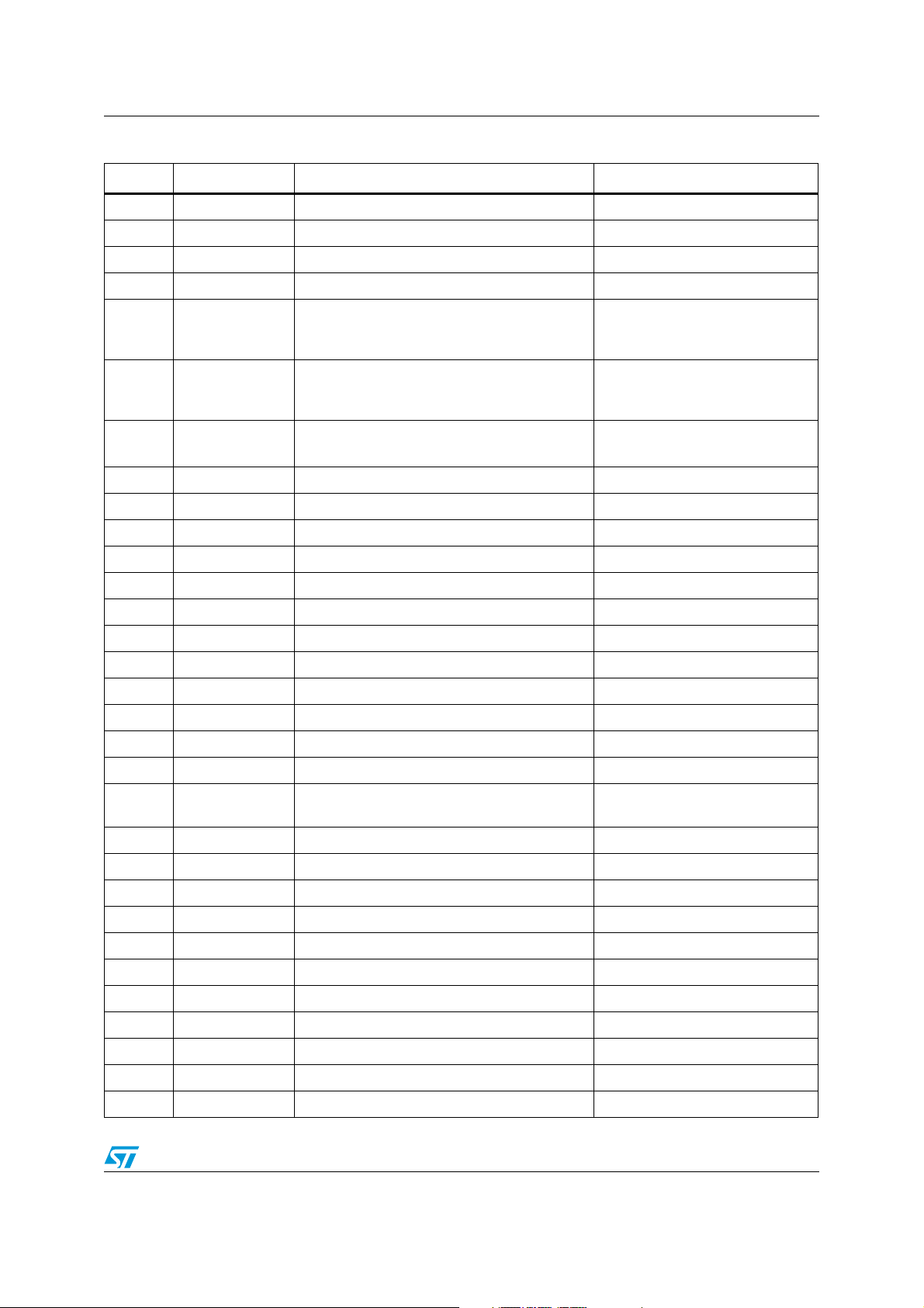
Table 2. Pin list . . . . . . . . . . . . . . . . . . . . . . . . . . . . . . . . . . . . . . . . . . . . . . . . . . . . . . . . . . . . . . . . . . 9
Table 3. Absolute maximum ratings . . . . . . . . . . . . . . . . . . . . . . . . . . . . . . . . . . . . . . . . . . . . . . . . . 11
Table 4. Operating conditions . . . . . . . . . . . . . . . . . . . . . . . . . . . . . . . . . . . . . . . . . . . . . . . . . . . . . . 12
Table 5. Digital logic levels . . . . . . . . . . . . . . . . . . . . . . . . . . . . . . . . . . . . . . . . . . . . . . . . . . . . . . . . 13
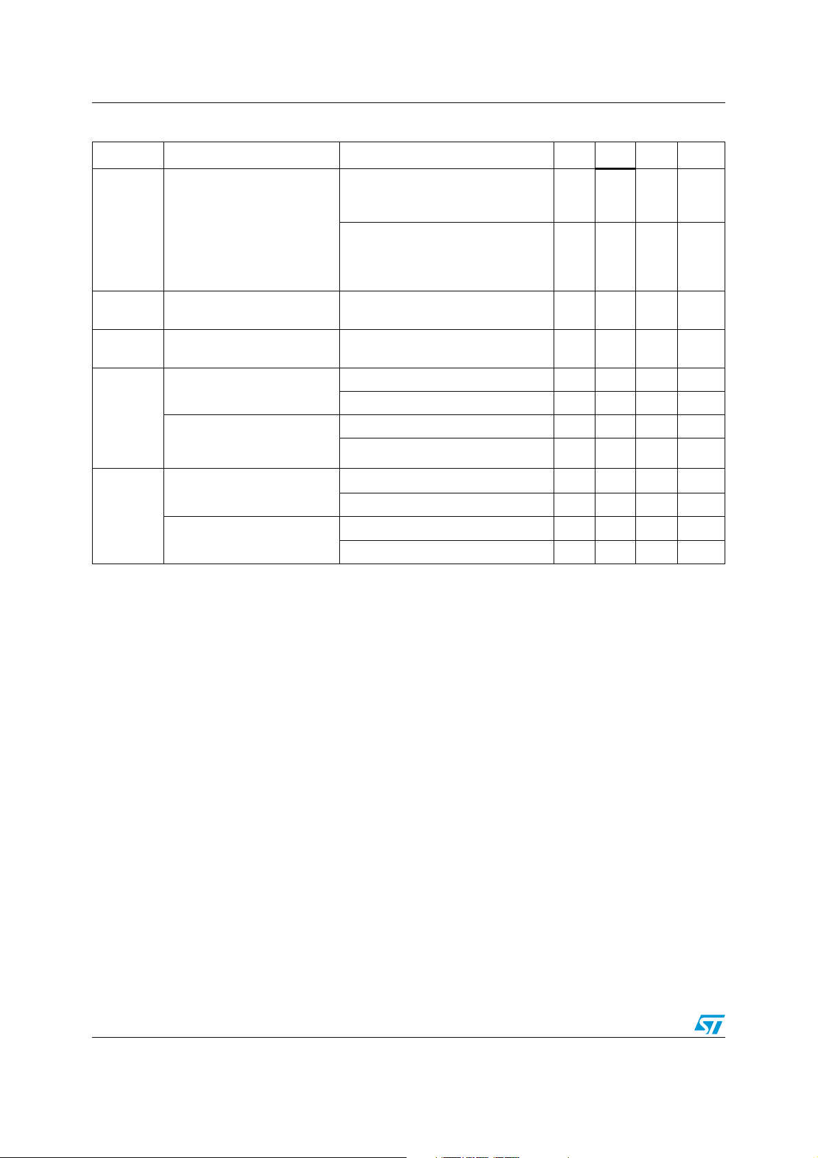
Table 6. Down converter mixer and IF amplifier electrical characteristics . . . . . . . . . . . . . . . . . . . . 15
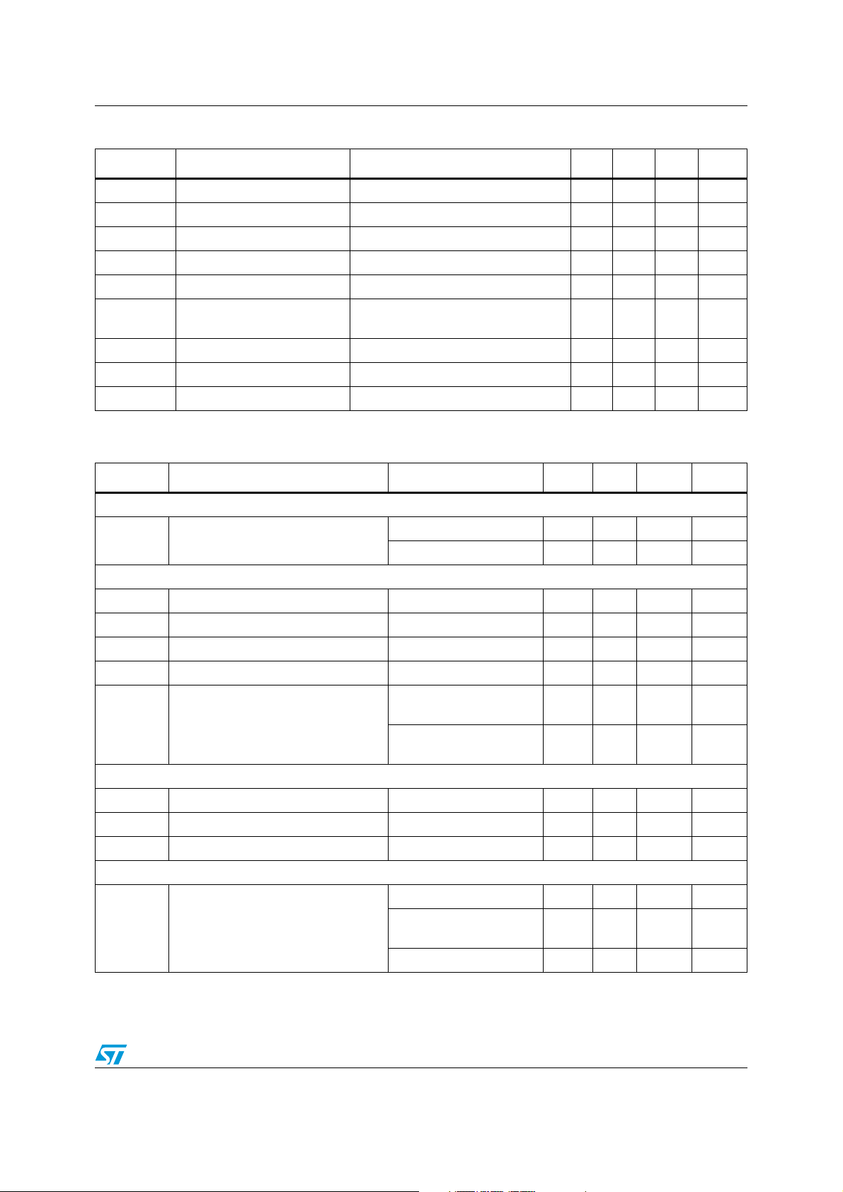
Table 7. Pin diode attenuator driver (dual output current DAC) electrical characteristics. . . . . . . . . 17
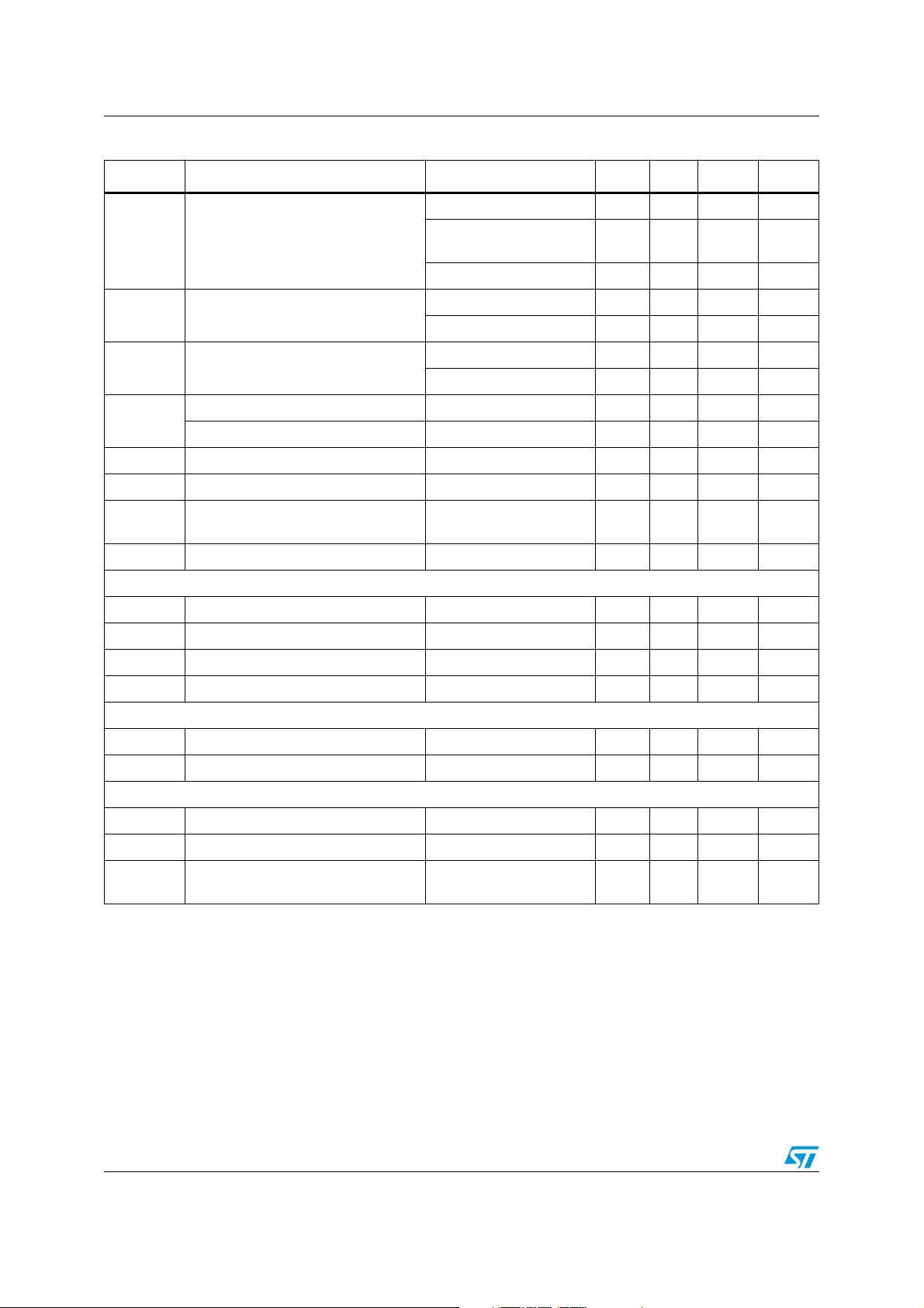
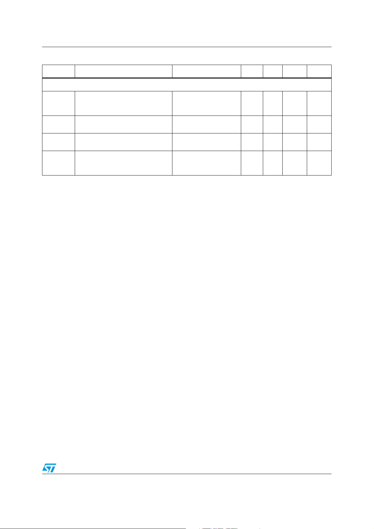
Table 8. Integer-N synthesizer electrical characteristics. . . . . . . . . . . . . . . . . . . . . . . . . . . . . . . . . . 17
Table 9. Phase noise performance . . . . . . . . . . . . . . . . . . . . . . . . . . . . . . . . . . . . . . . . . . . . . . . . . . 20
Table 10. Current values for CPSEL[2:0] selection . . . . . . . . . . . . . . . . . . . . . . . . . . . . . . . . . . . . . . 27
Table 11. VCOA performance against amplitude setting (frequency = 3.6 GHz) . . . . . . . . . . . . . . . . 31
Table 12. VCOB performance against amplitude setting (frequency = 4.3 GHz) . . . . . . . . . . . . . . . . 31
Table 13. Linearity performance against IFAMP[1:0] configuration (typical condition) . . . . . . . . . . . . 33
Table 14. I
Table 15. I
Table 16. I
Table 17. I
Table 18. Address decoder and outputs . . . . . . . . . . . . . . . . . . . . . . . . . . . . . . . . . . . . . . . . . . . . . . . 49
Table 19. SPI timing parameters . . . . . . . . . . . . . . . . . . . . . . . . . . . . . . . . . . . . . . . . . . . . . . . . . . . . 50
Table 20. SPI register list . . . . . . . . . . . . . . . . . . . . . . . . . . . . . . . . . . . . . . . . . . . . . . . . . . . . . . . . . . 51
Table 21. Application circuit component values . . . . . . . . . . . . . . . . . . . . . . . . . . . . . . . . . . . . . . . . . 57
Table 22. Evaluation kit order code . . . . . . . . . . . . . . . . . . . . . . . . . . . . . . . . . . . . . . . . . . . . . . . . . . 63
Table 23. VFQFPN-44 package dimensions . . . . . . . . . . . . . . . . . . . . . . . . . . . . . . . . . . . . . . . . . . . 65
Table 24. Document revision history . . . . . . . . . . . . . . . . . . . . . . . . . . . . . . . . . . . . . . . . . . . . . . . . . 66
2
C data and clock timing parameters. . . . . . . . . . . . . . . . . . . . . . . . . . . . . . . . . . . . . . . . . 37
2
C START and STOP timing parameters . . . . . . . . . . . . . . . . . . . . . . . . . . . . . . . . . . . . . 38
2
C acknowledge timing parameters. . . . . . . . . . . . . . . . . . . . . . . . . . . . . . . . . . . . . . . . . . 38
2
C register list . . . . . . . . . . . . . . . . . . . . . . . . . . . . . . . . . . . . . . . . . . . . . . . . . . . . . . . . . . 39
Doc ID 018503 Rev 3 5/68
Page 6

List of figures STW82101B
List of figures
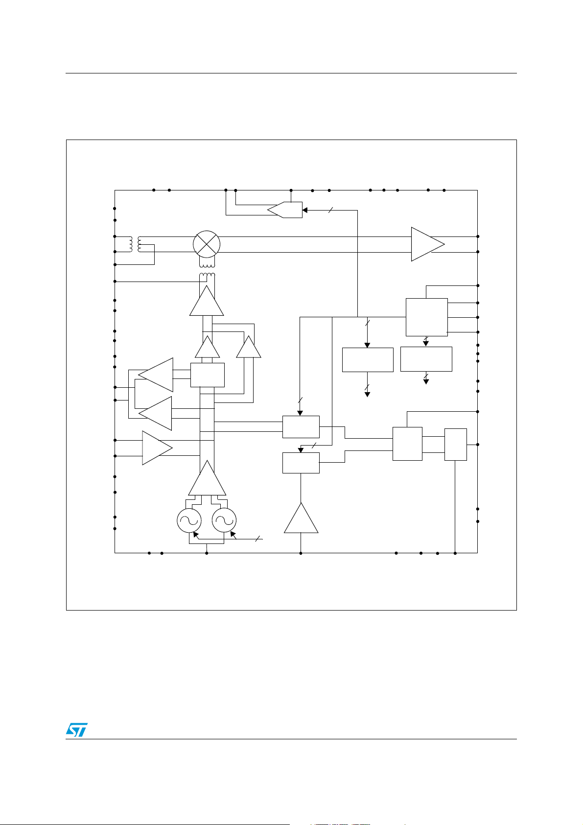
Figure 1. STW82101B block diagram . . . . . . . . . . . . . . . . . . . . . . . . . . . . . . . . . . . . . . . . . . . . . . . . . 7
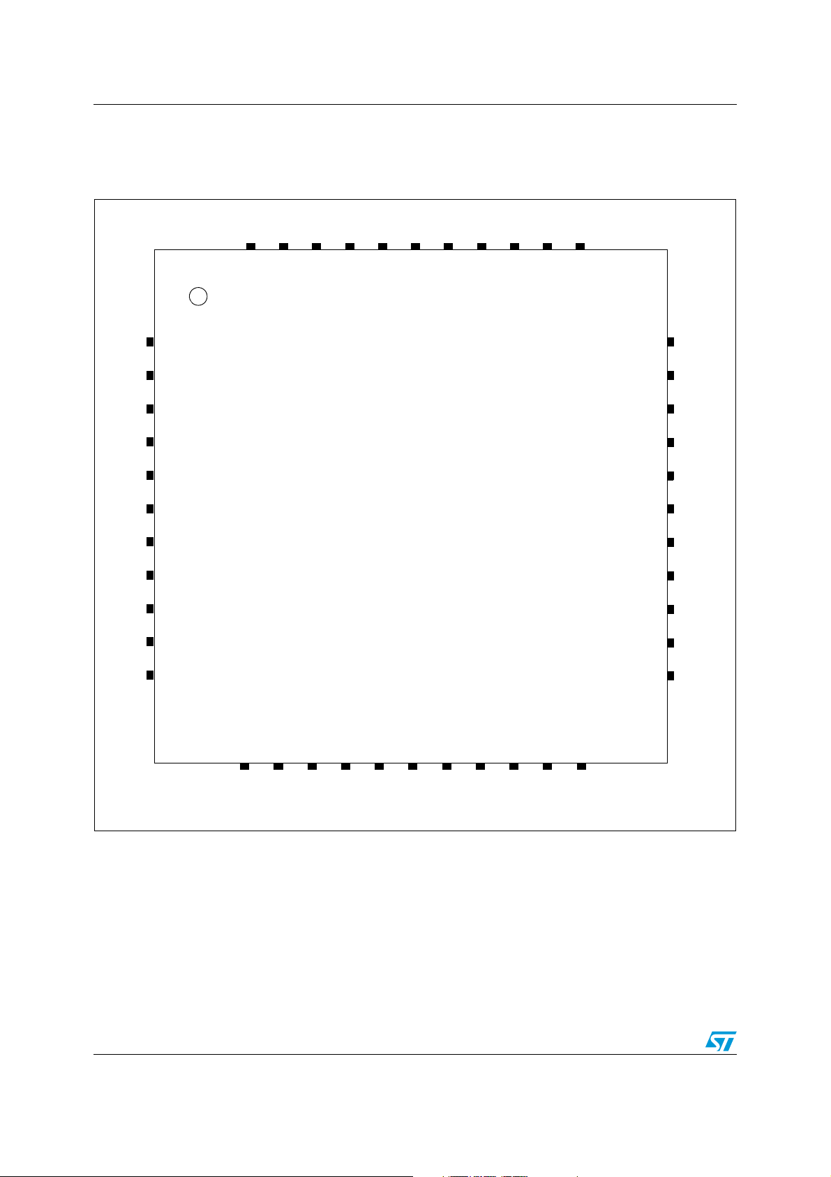
Figure 2. STW82101B pin configuration . . . . . . . . . . . . . . . . . . . . . . . . . . . . . . . . . . . . . . . . . . . . . . . 8
Figure 3. Conversion gain against RF frequency. . . . . . . . . . . . . . . . . . . . . . . . . . . . . . . . . . . . . . . . 21
Figure 4. Noise figure against RF frequency . . . . . . . . . . . . . . . . . . . . . . . . . . . . . . . . . . . . . . . . . . . 21
Figure 5. IIP3 against RF frequency . . . . . . . . . . . . . . . . . . . . . . . . . . . . . . . . . . . . . . . . . . . . . . . . . 22
Figure 6. 2RF-2LO response against RF frequency . . . . . . . . . . . . . . . . . . . . . . . . . . . . . . . . . . . . . 22
Figure 7. LOA (VCOA div. by 4) closed-loop phase noise at 0.94 GHz
(F
Figure 8. LOB (VCOB div. by 4) closed-loop phase noise at 1.1 GHz
(F
Figure 9. Reference frequency input buffer . . . . . . . . . . . . . . . . . . . . . . . . . . . . . . . . . . . . . . . . . . . . 24
Figure 10. VCO divider diagram . . . . . . . . . . . . . . . . . . . . . . . . . . . . . . . . . . . . . . . . . . . . . . . . . . . . . 26
Figure 11. PFD diagram. . . . . . . . . . . . . . . . . . . . . . . . . . . . . . . . . . . . . . . . . . . . . . . . . . . . . . . . . . . . 26
Figure 12. Loop filter connection . . . . . . . . . . . . . . . . . . . . . . . . . . . . . . . . . . . . . . . . . . . . . . . . . . . . . 28
Figure 13. VCO typical sub-band characteristics. . . . . . . . . . . . . . . . . . . . . . . . . . . . . . . . . . . . . . . . . 29
Figure 14. Data validity waveform . . . . . . . . . . . . . . . . . . . . . . . . . . . . . . . . . . . . . . . . . . . . . . . . . . . . 34
Figure 15. START and STOP condition waveform . . . . . . . . . . . . . . . . . . . . . . . . . . . . . . . . . . . . . . . 35
Figure 16. Byte format and acknowledge waveform . . . . . . . . . . . . . . . . . . . . . . . . . . . . . . . . . . . . . . 35
Figure 17. I
Figure 18. I
Figure 19. I
Figure 20. I2C first programming timing . . . . . . . . . . . . . . . . . . . . . . . . . . . . . . . . . . . . . . . . . . . . . . . 47
Figure 21. SPI input and output bit order . . . . . . . . . . . . . . . . . . . . . . . . . . . . . . . . . . . . . . . . . . . . . . . 48
Figure 22. SPI data structure . . . . . . . . . . . . . . . . . . . . . . . . . . . . . . . . . . . . . . . . . . . . . . . . . . . . . . . . 49
Figure 23. SPI timing waveforms . . . . . . . . . . . . . . . . . . . . . . . . . . . . . . . . . . . . . . . . . . . . . . . . . . . . . 50
Figure 24. SPI first programming timing . . . . . . . . . . . . . . . . . . . . . . . . . . . . . . . . . . . . . . . . . . . . . . . 55
Figure 25. Typical STW82101B application circuit . . . . . . . . . . . . . . . . . . . . . . . . . . . . . . . . . . . . . . . 56
Figure 26. Standard mode operation . . . . . . . . . . . . . . . . . . . . . . . . . . . . . . . . . . . . . . . . . . . . . . . . . . 58
Figure 27. Diversity mode operation with same LO frequencies . . . . . . . . . . . . . . . . . . . . . . . . . . . . . 59
Figure 28. Diversity mode operation with different LO frequencies . . . . . . . . . . . . . . . . . . . . . . . . . . . 60
Figure 29. External VCO standard mode operation . . . . . . . . . . . . . . . . . . . . . . . . . . . . . . . . . . . . . . . 61
Figure 30. External VCO diversity mode operation with same LO. . . . . . . . . . . . . . . . . . . . . . . . . . . . 62
Figure 31. VFQFPN-44 package outline . . . . . . . . . . . . . . . . . . . . . . . . . . . . . . . . . . . . . . . . . . . . . . . 64
= 200 kHz, ICP = 1.5 mA) . . . . . . . . . . . . . . . . . . . . . . . . . . . . . . . . . . . . . . . . . . . . 23
STEP
= 200 kHz, ICP = 1.5 mA) . . . . . . . . . . . . . . . . . . . . . . . . . . . . . . . . . . . . . . . . . . . . 23
STEP
2
C data and clock waveforms . . . . . . . . . . . . . . . . . . . . . . . . . . . . . . . . . . . . . . . . . . . . . . 37
2
C START and STOP timing waveforms . . . . . . . . . . . . . . . . . . . . . . . . . . . . . . . . . . . . . . 37
2
C acknowledge timing waveforms . . . . . . . . . . . . . . . . . . . . . . . . . . . . . . . . . . . . . . . . . . 38
6/68 Doc ID 018503 Rev 3
Page 7
STW82101B Block diagram
1 Block diagram
Figure 1. STW82101B block diagram
VDD_DAC
VDD_ALC
VSS_ALC
I_PINDRV1
I_PINDRV2
REXT_DAC
VSS_DAC
TEST_ALC
TEST2
TEST1
VDD_IFAMP
VSS_IFAMP
VDD_RFESD
VSS_RFESD
RF_IN
RF_VSS
RF_CT
MIXDRV_CT
VDD_MIXDRV
VSS_MIXDRV
VDD_DIV
VSS_DIV
VDD_OUTBUF
VSS_OUTBUF
OUTBUFN
OUTBUFP
EXTVCO_INP
EXTVCO_INN
VDD_VCO
VSS_VCO
VDD_IO
VSS_IO
LO
OUT
LO/4xLO
OUT
EXT
LO/VCO
BUF
MIX
DRV
DIV4
VCO
BUFF
CAL_VCO
DAC
VCO
divider
REF
divider
BUF
VCO
calibrator
CAL_VCO
Power down
PFD
IF
AMP
DBUS
decoder
PD<4:0>
Power
downs
UP
DN
CHP
IF_OUTP
IF_OUTN
DBUS_SEL
SDA/DATA
SCL/CLK
LOAD
ADD0
ADD1
ADD2
VDD_DIG
VSS_DIG
LOCK_DET
ICP
VDD_PLL
VSS_PLL
VDD_PSCBUF
VSS_PSCBUF
VCTRL
REF_CLK
EXT_PD
VSS_CP
VDD_CP
REXT_CP
Doc ID 018503 Rev 3 7/68
Page 8
Pin description STW82101B
2 Pin description
Figure 2. STW82101B pin configuration
44 43 42 41 40 39 38 37 36 35 34
10
11
1
2
3
4
5
6
7
8
9
VDD_DAC
REXT_DAC
VDD_DIV
VDD_VCO
EXTVCO_INN
EXTVCO_INP
EXT_PD
ADD2
ADD1
ADD0
VDD_IO
RF_IN
RF_CT
VDD_MIXDRV
VDD_ALC
MIXDRV_CT
VDD_RFESD
I_PINDRV1
I_PINDRV2
TEST_ALC
TEST1
TEST2
VDD_IFAMP
IF_OUTP
IF_OUTN
NC
LOAD
33
32
31
30
29
STW82101B
VFQFPN44
SCL/CLK
SDA/DATA
VDD_DIG
DBUS_SEL
VDD_PLL
REF_CLK
28
27
26
25
24
23
VDD_PSCBUF
NC
NC
VDD_OUTBUF
OUTBUFN
OUTBUFP
VCTRL
12 13 14 15 16 17 18 19 20 21 22
8/68 Doc ID 018503 Rev 3
ICP
REXT_CP
VDD_CP
LOCK_DET
Page 9
STW82101B Pin description
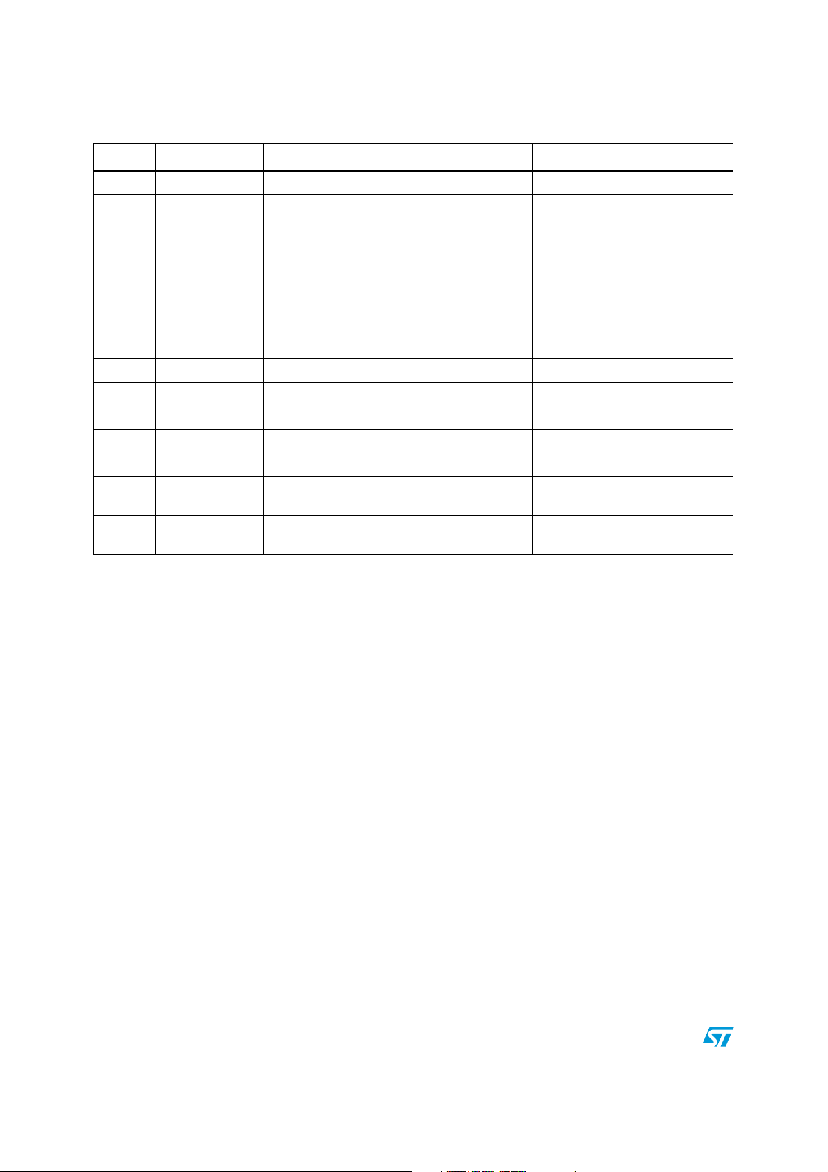
Table 2. Pin list
Pin No Name Description Observation
1 VDD_DAC DAC power supply Vsupply analog1= 3.3 V
2 REXT_DAC External resistance connection for DAC -
3 VDD_DIV Divider by 4 power supply Vsupply analog1= 3.3 V
4 VDD_VCO VCOs and External VCO Buffer power supply Vsupply analog1= 3.3 V
Diversity Slave Mode and External
5 EXTVCO_INN External VCO (LO) negative input
6 EXTVCO_INP External VCO (LO) positive input
7 EXT_PD
8 ADD2 I
9 ADD1 I
10 ADD0 I
Hardware power down:
‘0’ device ON; ‘1’ device OFF
2
CBUS address select pin CMOS Input
2
CBUS address select pin CMOS Input
2
CBUS address select pin CMOS Input
11 VDD_IO Digital IO power supply Vsupply digital = 3.3 V
12 VDD_PSCBUF Prescaler input buffer power supply Vsupply analog1= 3.3 V
13 NC Not connected -
VCO Modes; otherwise it must be
connected to GND
Diversity Slave Mode and External
VCO Modes; otherwise it must be
connected to GND
CMOS Input
14 NC Not connected -
15 VDD_OUTBUF Power supply for LO buffer Vsupply analog1=3.3 V
16 OUTBUFN LO Output buffer negative output Open collector @3.3 V
17 OUTBUFP LO Output buffer positive output Open collector @ 3.3 V
18 VCTRL Control voltage for VCOs -
19 ICP PLL charge pump output -
20 REXT_CP
External resistance connection for PLL charge
pump current
-
21 VDD_CP Power supply for charge pump Vsupply analog1= 3.3 V
22 LOCK_DET Lock detector CMOS Output
23 REF_CLK Reference frequency input -
24 VDD_PLL PLL digital power supply Vsupply analog1= 3.3 V
25 DBUS_SEL Digital Bus Interface select CMOS Input
26 VDD_DIG Power supply for digital bus interface Vsupply digital = 3.3 V
2
27 SDA/DATA I
28 SCL/CLK I
CBUS /SPI data line CMOS Bidir Schmitt triggered
2
CBUS /SPI clock line CMOS Input Schmitt triggered
29 LOAD SPI load line CMOS Input Schmitt triggered
30 NC Not connected -
31 IF_OUTN IF amplifier negative output Open collector @ 5 V
(1)
Doc ID 018503 Rev 3 9/68
Page 10
Pin description STW82101B
Table 2. Pin list (continued)
Pin No Name Description Observation
32 IF_OUTP IF Amplifier positive output Open collector @ 5 V
33 VDD_IFAMP IF Amplifier power supply Vsupply analog1 = 3.3 V
34 TEST2 Test input 2
35 TEST1 Test input 1
Test purpose only; it must be
connected to GND
Test purpose only; it must be
connected to GND
(1)
36 TEST_ALC Test output
Test purpose only; it must be
connected to GND
37 RF_CT RF balun central tap -
38 RF_IN RF input -
39 VDD_RFESD RF ESD positive rail power supply Vsupply analog1 = 3.3 V
40 MIXDRV_CT Mixer driver balun central tap Vsupply analog2 = 5 V
41 VDD_ALC ALC power supply Vsupply analog1 = 3.3 V
42 VDD_MIXDRV Mixer driver power supply Vsupply analog1 = 3.3 V
43 I_PINDRV1
44 I_PINDRV2
1. Supply voltage @ 3.3 V in low-current mode operation
DAC current output for external PIN Diode
attenuator
DAC current output for external PIN Diode
attenuator
PMOS Open drain
PMOS Open drain
(1)
10/68 Doc ID 018503 Rev 3
Page 11
STW82101B Absolute maximum ratings
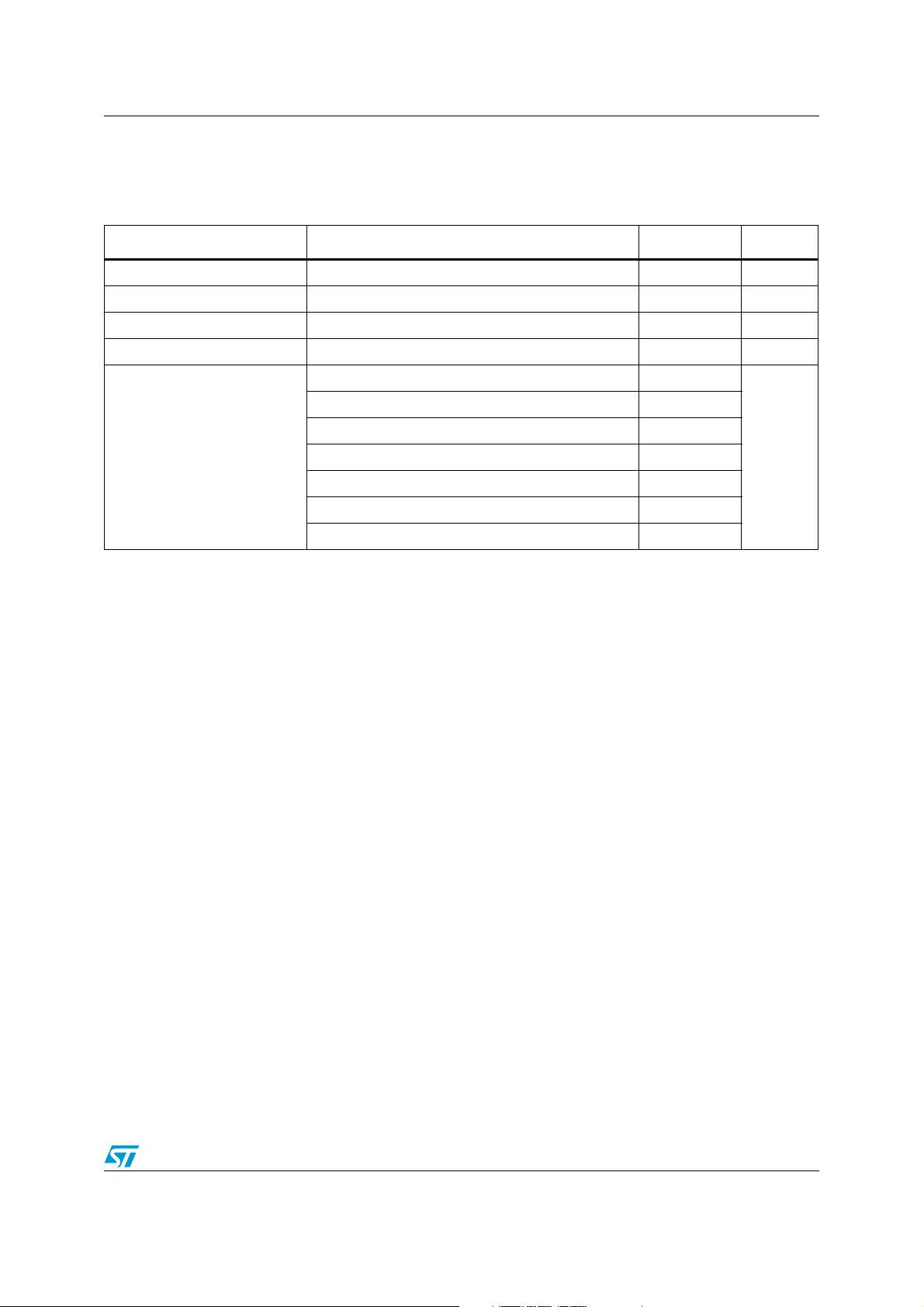
3 Absolute maximum ratings
Table 3. Absolute maximum ratings
Symbol Parameter Values Unit
AVCC1 Analog Supply voltage 0 to 4.6 V
AVCC2 Analog Supply voltage 0 to 6 V
DVCC Digital Supply voltage 0 to 4.6 V
Tstg Storage temperature +150 °C
HBM on pins 16, 17, 31, 32 0.8
HBM on pin 37, 38, 40 1
HBM on all remaining pins 2
ESD
(Electro-static discharge)
CDM-JEDEC Standard on pin 38 0.25
CDM-JEDEC Standard on all remaining pins 0.5
MM on pins 16, 17 0.15
MM on all remaining pins 0.2
kV
Doc ID 018503 Rev 3 11/68
Page 12
Operating conditions STW82101B
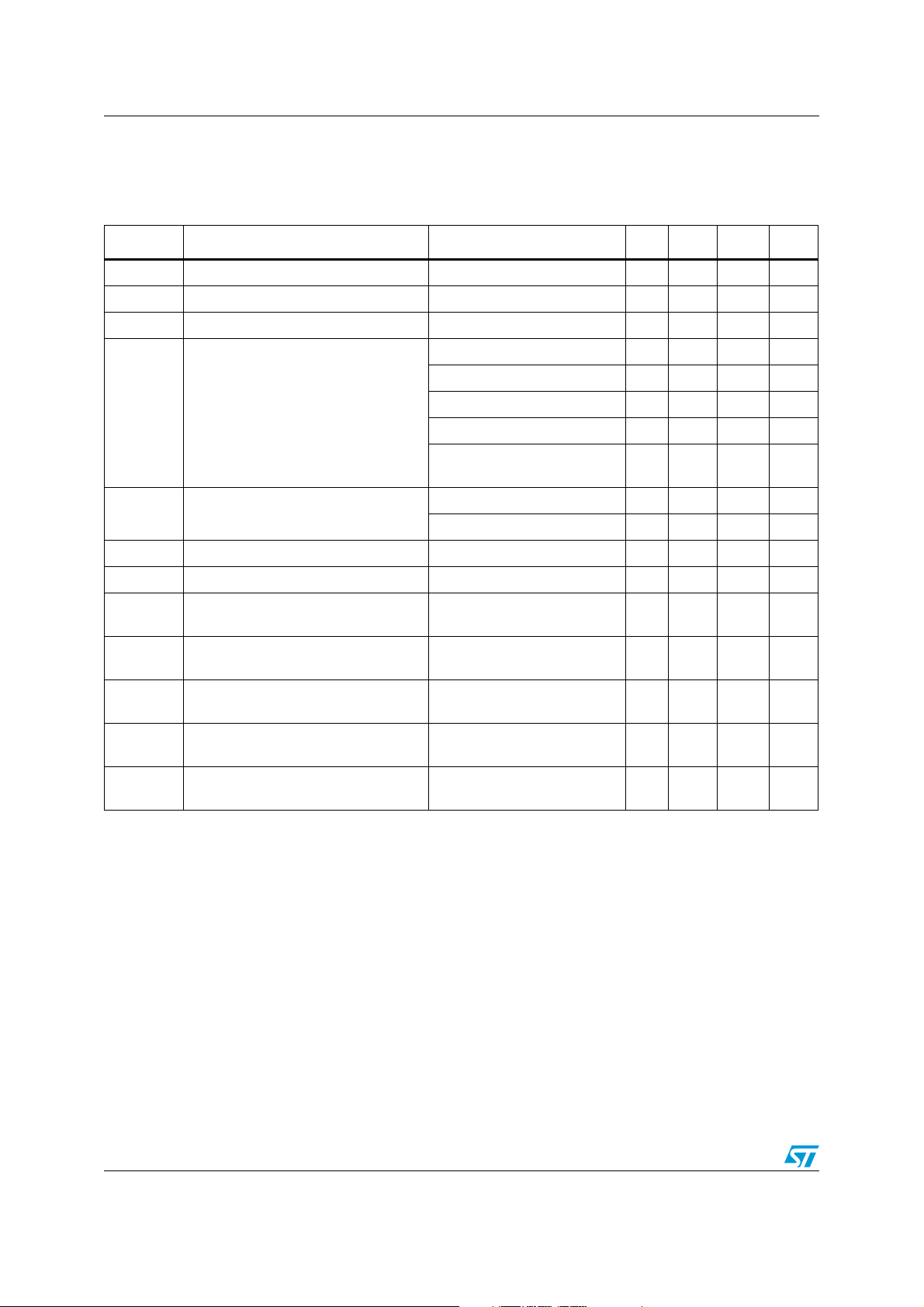
4 Operating conditions
Table 4. Operating conditions
Symbol Parameter Test conditions Min Typ Max Unit
AVCC1 Analog Supply voltage - 3.15 3.3 3.45 V
AVCC2 Analog Supply voltage - 4.75 5 5.25 V
DVCC Digital Supply voltage - 3.15 3.3 3.45 V
Standard mode - 110 127 mA
External VCO standard mode - 95 110 mA
I
CC3.3V
Current Consumption at 3.3 V
Diversity slave mode - 90 105 mA
Diversity master mode - 145 167 mA
External VCO diversity master
mode
- 140 160 mA
High current mode at 5 V - 140 160 mA
I
CC5V
T
A
T
J
Θ
JA
Θ
JB
Θ
JC
Ψ
JB
Current Consumption
Low current mode at 3.3 V - 80 90 mA
Operating ambient temperature - -40 85 °C
Maximum junction temperature - - 125 °C
Junction to ambient package thermal
resistance
Junction to board package thermal
resistance
Junction to case package thermal
resistance
Thermal characterization parameter
junction to board
(1)
(1)
(1)
(1)
Multi-layer JEDEC board - 33 - °C/W
Multi-layer JEDEC board - 19 - °C/W
Multi-layer JEDEC board - 3 - °C/W
Multi-layer JEDEC board - 18 - °C/W
Ψ
JT
1. Refer to JEDEC standard JESD 51-12 for a detailed description of the thermal resistances and thermal parameters.
Data here presented are referring to a Multi-layer board according to JEDEC standard.
T
= TA + ΘJA * Pdiss (in order to estimate TJ if ambient temperature TA and dissipated power Pdiss are known)
J
T
= TB + ΨJB * Pdiss (in order to estimate TJ if board temperature TB and dissipated power Pdiss are known)
J
T
= TT + ΨJT * Pdiss (in order to estimate TJ if top case temperature TT and dissipated power Pdiss are known)
J
Thermal characterization parameter
junction to top case
(1)
Multi-layer JEDEC board - 0.3 - °C/W
12/68 Doc ID 018503 Rev 3
Page 13

STW82101B Operating conditions
Table 5. Digital logic levels
T
Symbol Parameter Test conditions Min Typ Max Unit
Vil Low level input voltage - - - 0.2*Vdd V
Vih High level input voltage - 0.8*Vdd - - V
Vhyst Schmitt trigger hysteresis - 0.8 - - V
Vol Low level output voltage - - - 0.4 V
Voh High level output voltage - 0.85*Vdd - - V
Doc ID 018503 Rev 3 13/68
Page 14

Test conditions STW82101B
5 Test conditions
Unless otherwise specified the following test conditions are applied:
● Vsupply digital = 3.3 V
● Vsupply analog1 = 3.3 V
● Vsupply analog2 = 5 V
● F
● MIX = 0111
● T ambient = 27 ° C
Refer also to Section 11: Application information.
= 150 MHz
IF
14/68 Doc ID 018503 Rev 3
Page 15
STW82101B Electrical characteristics
6 Electrical characteristics
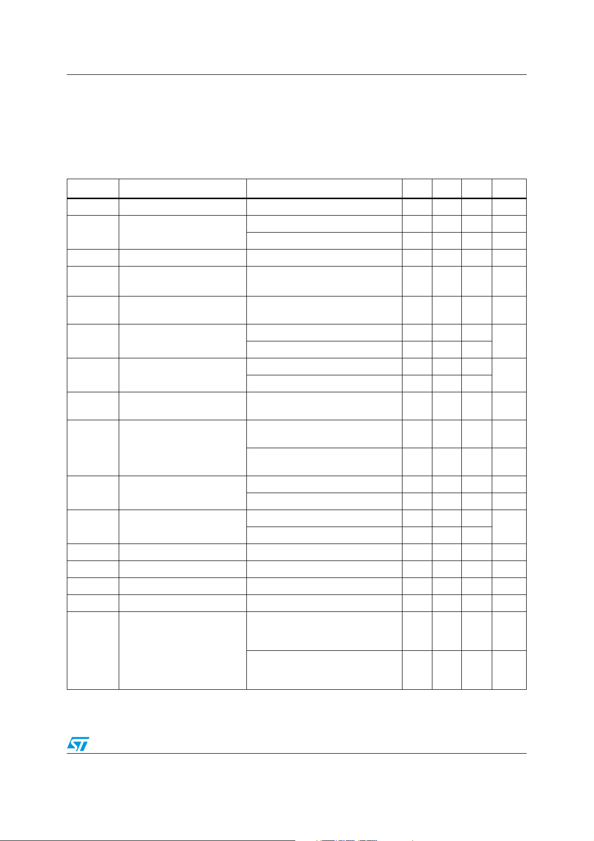
Note: Vsupply digital = 3.3 V, Vsupply analog1 = 3.3 V, Vsupply analog2 = 5 V, FRF = 800 MHz,
FLO = 950 MHz, TA = +25*C, RF power = 0 dBm, unless otherwise specified.
Table 6. Down converter mixer and IF amplifier electrical characteristics
)
(1)
Symbol Parameter Conditions Min Typ Max Unit
F
RF
F
LO
F
IF
CG Power Conversion Gain
CG
ΔT
IP
1dB
IIP3
IIP3
ΔT
RF Frequency - 695 - 960 MHz
VCOA divided by 4 850 - 1025 MHz
LO Frequency
VCOB divided by 4 1025 - 1185 MHz
IF Center Frequency
Power Conversion Gain over
Temperature
(3)
(2)
FIF = ABS(FLO-FRF)70-400MHz
Rin = 50 ohm, Rout = 200 ohm
RFin = 0 dBm
88.59dB
T= -40 to +85 °C - ±0.6 - dB
High current Mode - 12 -
Input P1dB
dBm
Low current Mode - 7 -
Third-order input intercept
(4)
point
IIP3 variation over
temperature
(3)
High current Mode 24 24.5 -
dBm
Low current Mode 18 18.5 -
T= -40 to +85 °C - ±0.5 - dB
2F
nFRF-nFLOSpurious rejection at IF
(3)
-2FLO F
RF
F
= 150 MHz
IF
-3FLO F
3F
RF
= 150 MHz
F
IF
RFin
RFin
= -5 dBm,
= -5 dBm,
-75-dBc
-75-dBc
High-current mode, MIX = 0011 - 9.5 10.2 dB
NF
SSB
Noise figure
Low-current mode, MIX = 0011 - 9.5 10.2 dB
1xLO - -20 -
- LO to IF Leakage
dBm
2xLO -30
- LO to RF Leakage - - -27 - dBm
- RF to IF Isolation - - 55 - dB
RF
IF
RL
RL
RF Return Loss Matched to 50 ohm - 20 - dB
IF Return Loss Matched to 200 ohm - 22 - dB
Maximum deviation from Fc over
±10 MHz. For any Fc within each TX
-
observation path
(5)
Gain Flatness for TX
observation path band.
Maximum deviation from F
over
c
±17.5 MHz. For any Fc within each
-0.05 - +0.05 dB
-0.10 - +0.10 dB
TX observation path band.
Doc ID 018503 Rev 3 15/68
Page 16
Electrical characteristics STW82101B
Table 6. Down converter mixer and IF amplifier electrical characteristics
(1)
(continued)
Symbol Parameter Conditions Min Typ Max Unit
Maximum deviation from linear phase
at F
over ±10 MHz. For any Fc within
c
each TX observation path band.
-
Phase Flatness for TX
observation path
(5)
Maximum deviation from linear phase
at F
over ±17.5 MHz. For any Fc
c
within each TX observation path
band.
Maximum ripple over a 4 MHz band.
(5)
- Gain Flatness for RX path
- Phase Flatness for RX path
Mixer Driver Current
Consumption
ICC
MD
Mixer Driver Current
For any F
Maximum ripple over a 4 MHz band.
(5)
within each RX path band.
c
For any Fc within each RX path band.
3.3 V Supply (pin 41, 42) - 35 - mA
5 V Supply (pin 40) - 35 - mA
3.3 V Supply (pin 41, 42) - 20 - mA
Consumption (Low Current
Mode)
3.3 V Supply (pin 40) - 20 - mA
3.3 V Supply (pin 33) - 10 - mA
IFAMP Current Consumption
5 V Supply (pin 31, 32) - 107 - mA
ICC
IFAM
IFAMP Current Consumption
(Low Current Mode)
1. All linearity and NF performances are intended at maximum LO amplitude (LO_A[1:0]=[11]), tuning capacitors (CAP[2:0])
programmed according to the selected frequency, mixer bias (MIX[3:0]) set to maximize performance and the device
operated in high current mode. The performances of conversion gain, NF and linearity are intended at the SMA connectors
of a typical application board.
2. The IF frequency range supported by the IF Amplifier is from 70 to 400 MHz. The exact IF frequency range supported for a
specific RF frequency can be calculated as F
3. Guaranteed by design and characterization
4. RFin = 0 dBm/tone, RF tone spacing = 5 MHz
5. Guaranteed by design
3.3 V Supply (pin 33) - 6 - mA
3.3 V Supply (pin 31, 32) - 55 - mA
= ABS(FLO-FRF) where FLO is inside the specified LO frequency range.
IF
-0.3 - +0.3 deg
-0.7 - +0.7 deg
--0.1
--0.6
dB
pk-pk
deg
pk-pk
16/68 Doc ID 018503 Rev 3
Page 17
STW82101B Electrical characteristics
Table 7. Pin diode attenuator driver (dual output current DAC) electrical characteristics
Symbol Parameters
Conditions Min Typ Max Unit
R Resolution - - 10 - Bit
DNL Differential non linearity - -0.05 - 0.05 LSB
INL Integral non linearity - -0.45 - 0.45 LSB
I
FS
Full Scale current
(1)
-0.28-2.8mA
- Current Mismatch - - - 2 %
-
VR
EXT_DAC
R
EXT_DAC
Icc
static
1. See relationship between IDAC and R
Table 8. Integer-N synthesizer electrical characteristics
Output voltage compliance
range
-0-3V
Voltage Reference - - 1.19 V
REXT DAC Range - 10 - 100 kΩ
Static current consumption (Iout = 0 mA; pin 1) - 2.5 - mA
in the Circuit Description section (Dual Output Current DAC)
EXT_DAC
Symbol Parameter Conditions Min Typ Max Unit
VCO dividers
Prescaler 16/17 256 - 65551 -
N VCO Divider Ratio (N)
Prescaler 19/20 361 - 77836 -
Reference clock and phase frequency detector
F
ref
Reference input frequency - 10 19.2 200 MHz
- Reference input sensitivity - 0.35 1 1.5 Vpeak
R Reference Divider Ratio - 2 - 1023
F
PFD
F
STEP
PFD input frequency - - - 16 MHz
Frequency step
(1)
Prescaler 16/17
Prescaler 19/20
F
LO
65551
F
LO
77836
/
/
FLO/
256
FLO/
361
Hz
Hz
Charge pump
I
V
CP
OCP
ICP sink/source
Output voltage compliance range - 0.4 - Vdd-0.3 V
- Spurious
(3)
(2)
3bit programmable - - 5 mA
---70-dBc
VCOs
Higher frequency range - 90 - MHz/V
K
VCOA
VCOA sensitivity
Intermediate frequency
range
- 70 - MHz/V
Lower frequency range - 60 - MHz/V
Doc ID 018503 Rev 3 17/68
Page 18
Electrical characteristics STW82101B
Table 8. Integer-N synthesizer electrical characteristics (continued)
Symbol Parameter Conditions Min Typ Max Unit
Higher frequency range - 75 - MHz/V
K
VCOB
VCOB sensitivity
Intermediate frequency
range
- 65 - MHz/V
Lower frequency range - 55 - MHz/V
ΔT
ΔT
LKA
LKB
VCOA maximum temperature
variation for continuous lock
VCOB maximum temperature
variation for continuous lock
(4)
(4)
)
CALTYPE [0] 100 ° C
CALTYPE [1] 125 ° C
CALTYPE [0] 95 ° C
CALTYPE [1] 125 ° C
VCO A Pushing - - 8 - MHz/V
VCO B Pushing - - 14 - MHz/V
V
CTRL
VCO control voltage - 0.4 Vdd-0.3 V
- LO Harmonic Spurious - - -20 dBc
I
VCO
IDIV
4
VCO and VCO buffer current
consumption
Amplitude [11] (pin 4) - 35 - mA
DIVIDER by 4 consumption (pin 3) - 17 - mA
4 x LO output buffer (test purpose only)
F
P
OUT
OUT
Frequency range - 3.4 - 4.74 GHz
Output level - - 0 - dBm
RL Return Loss Matched to 50ohm - 10 - dB
I
4LOBUF
Current Consumption (pin 15, 16, 17) - 26 - mA
LO output buffer
F
P
OUT
OUT
Frequency range - 0.85 - 1.185 GHz
Output level - - -1 - dBm
External VCO (LO) buffer
f
INVCO
P
IN
I
EXTBUF
Frequency range - 0.85 - 1.185 GHz
Input level - - 0 - dBm
Current Consumption
External VCO Buffer
(pin 4)
18/68 Doc ID 018503 Rev 3
-25 -mA
Page 19
STW82101B Electrical characteristics
Table 8. Integer-N synthesizer electrical characteristics (continued)
Symbol Parameter Conditions Min Typ Max Unit
PLL miscellaneous
Input Buffer, Prescaler,
I
PLL
I
PRE
I
CP
PLL Current Consumption
Prescaler input buffer Current
Consumption
Charge Pump Current Consumption
Digital Dividers, misc.
-8 -mA
(pin 24)
(pin 12) - 3 - mA
CPSEL=[111], REXT_CP
= 4.7 kΩ (pin 21)
-4 -mA
25 kHz PLL bandwidth;
within 1ppm of frequency
-150 -µs
t
LOCK
Lock up time
(5)
error
1. The frequency step is related to the PFD input frequency as follows: F
2. See relationship between ICP and R
3. The level of spurs may change depending on PFD frequency, Charge Pump current, selected channel and PLL loop BW.
4. When setting a specified output frequency, the VCO calibration procedure must be run first in order to select the best subrange for the VCO covering the desired frequency. Once programmed at the initial temperature T
temperature range (-40 ° C to +85 ° C), the synthesizer is able to maintain the lock status if the temperature drift (in either
direction) is within the limit specified by ΔTLK, provided that the final temperature T1 is still inside the nominal range.
5. Frequency jump form 1150 to 1075 MHz; it includes the time required by the VCO calibration procedure (7 x F
=17.5 µs with F
=400 kHz))
PFD
in the Circuit Description section (Charge Pump)
EXT_CP
STEP=FPFD
/2)
inside the operating
0
cycles
PFD
Doc ID 018503 Rev 3 19/68
Page 20
Electrical characteristics STW82101B
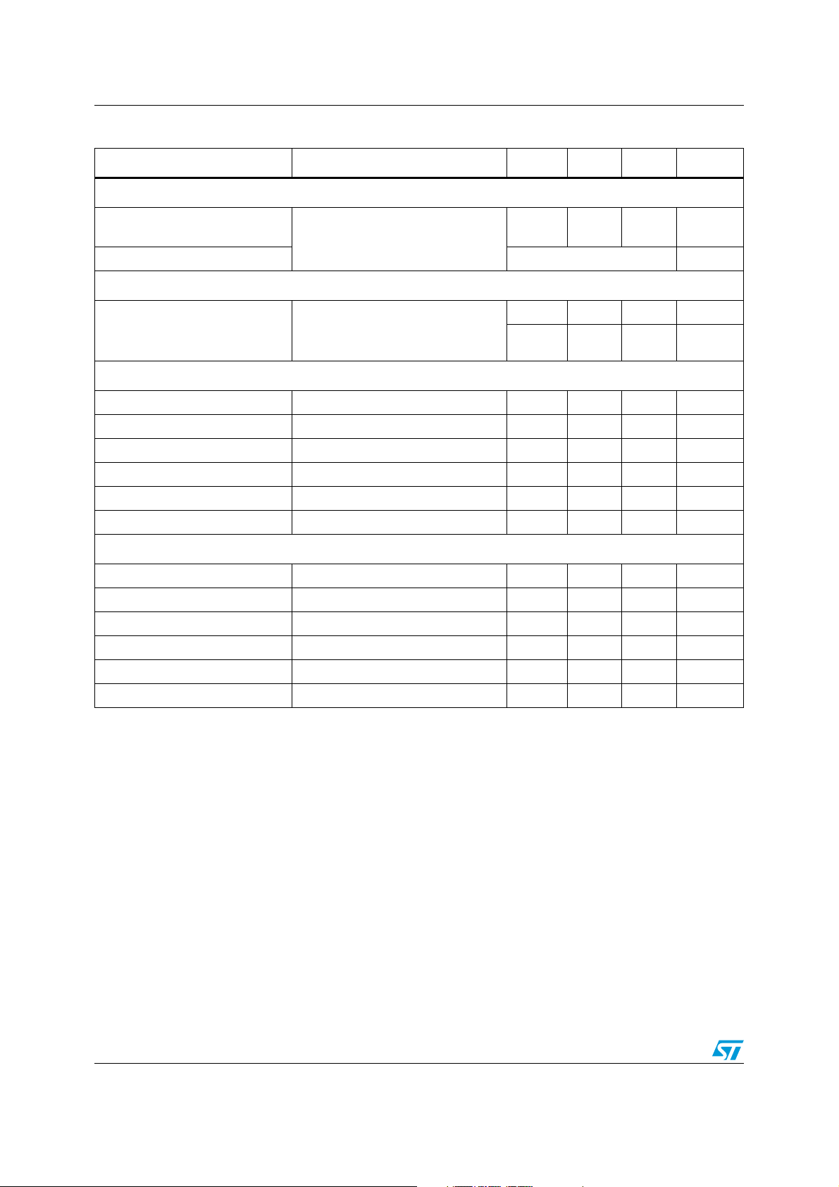
Table 9. Phase noise performance
(1)
Parameters Conditions Min. Typ. Max. Unit
In band phase noise floor, closed loop
Normalized In Band Phase Noise
Floor (LO)
In Band Phase Noise Floor (LO) -236+20log(N)+10log(F
(2)
I
=4 mA, PLL BW = 50 kHz
CP
(including reference clock
contribution)
--236-
) dBc/Hz
PFD
dBc/Hz
PLL integrated phase noise
Integrated Phase Noise
(single sided)
100 Hz to 40 MHz
= 1.075 GHz, F
F
LO
STEP
=200 kHz,
ICP = 3 mA, PLL BW = 25 kHz
--53.4-dBc
- 0.18 - ° rms
LOA (850 MHz to 1025 MHz) – open loop
Phase Noise @ 1 kHz - - -74 - dBc/Hz
Phase Noise @ 10 kHz - - -100 - dBc/Hz
Phase Noise @ 100 kHz - - -123 - dBc/Hz
Phase Noise @ 1 MHz - - -143 - dBc/Hz
Phase Noise @ 10 MHz - - -155 - dBc/Hz
Phase Noise Floor @ 40 MHz - - -156 - dBc/Hz
LOB (1025 MHz to 1185 MHz) – open loop
Phase Noise @ 1 kHz - - -67 - dBc/Hz
Phase Noise @ 10 kHz - - -95 - dBc/Hz
Phase Noise @ 100 kHz - - -118 - dBc/Hz
Phase Noise @ 1 MHz - - -140 - dBc/Hz
Phase Noise @ 10 MHz - - -154 - dBc/Hz
Phase Noise Floor @ 40 MHz - - -156 - dBc/Hz
1. Phase Noise SSB. VCO amplitude set to maximum value [11]. All the closed-loop performances are specified using a
Reference Clock signal at 76.8 MHz with phase noise of -144 dBc/Hz @1 kHz offset, -157 dBc/Hz @10 kHz offset and
-168 dBc/Hz of noise floor.
2. Normalized PN = Measured LO PN – 20log(N) – 10log(F
comparison frequency at the PFD input
) where N is the VCO divider ratio (N=B*P+A) and F
PFD
PFD
is the
20/68 Doc ID 018503 Rev 3
Page 21
STW82101B Typical performance characteristics
7 Typical performance characteristics
Note: Vsupply digital = 3.3 V, Vsupply analog1 = 3.3 V, Vsupply analog2 = 5 V, F
T
= +25 °C, RF power = 0 dBm, unless otherwise specified.
A
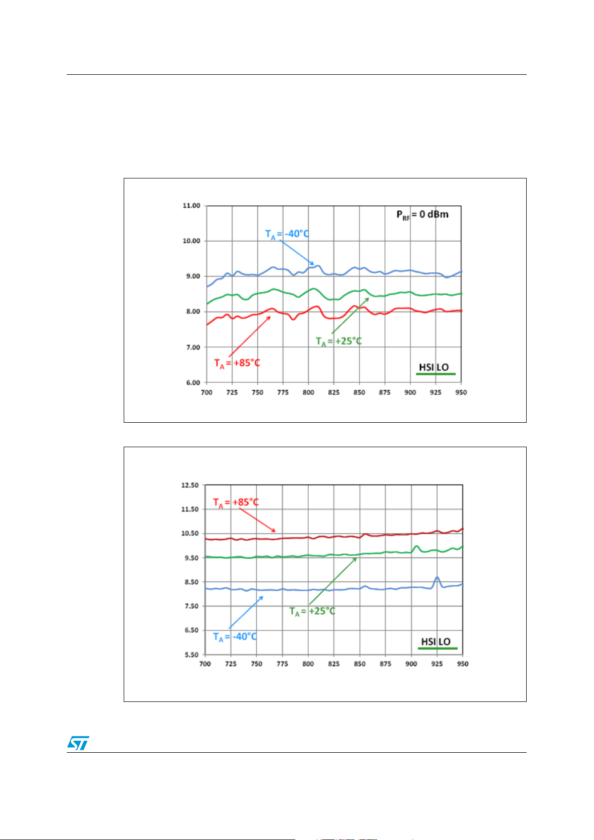
Figure 3. Conversion gain against RF frequency
Conversion gain (dB)
RF frequency (MHz)
= 150 MHz,
IF
Figure 4. Noise figure against RF frequency
Noise figure (dB)
RF frequency (MHz)
Doc ID 018503 Rev 3 21/68
Page 22
Typical performance characteristics STW82101B
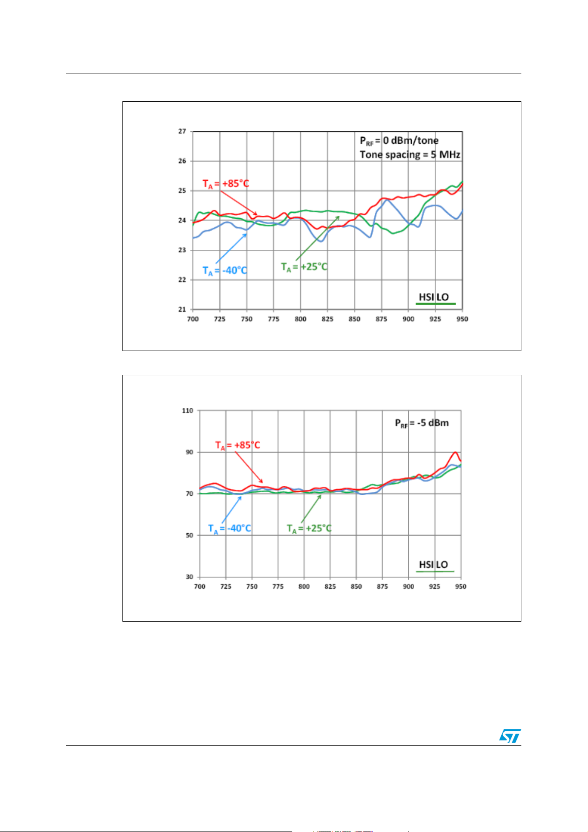
Figure 5. IIP3 against RF frequency
IIP3 (dBm)
RF frequency (MHz)
Figure 6. 2RF-2LO response against RF frequency
2RF-2LO response (dB)
RF frequency (MHz)
22/68 Doc ID 018503 Rev 3
Page 23
STW82101B Typical performance characteristics
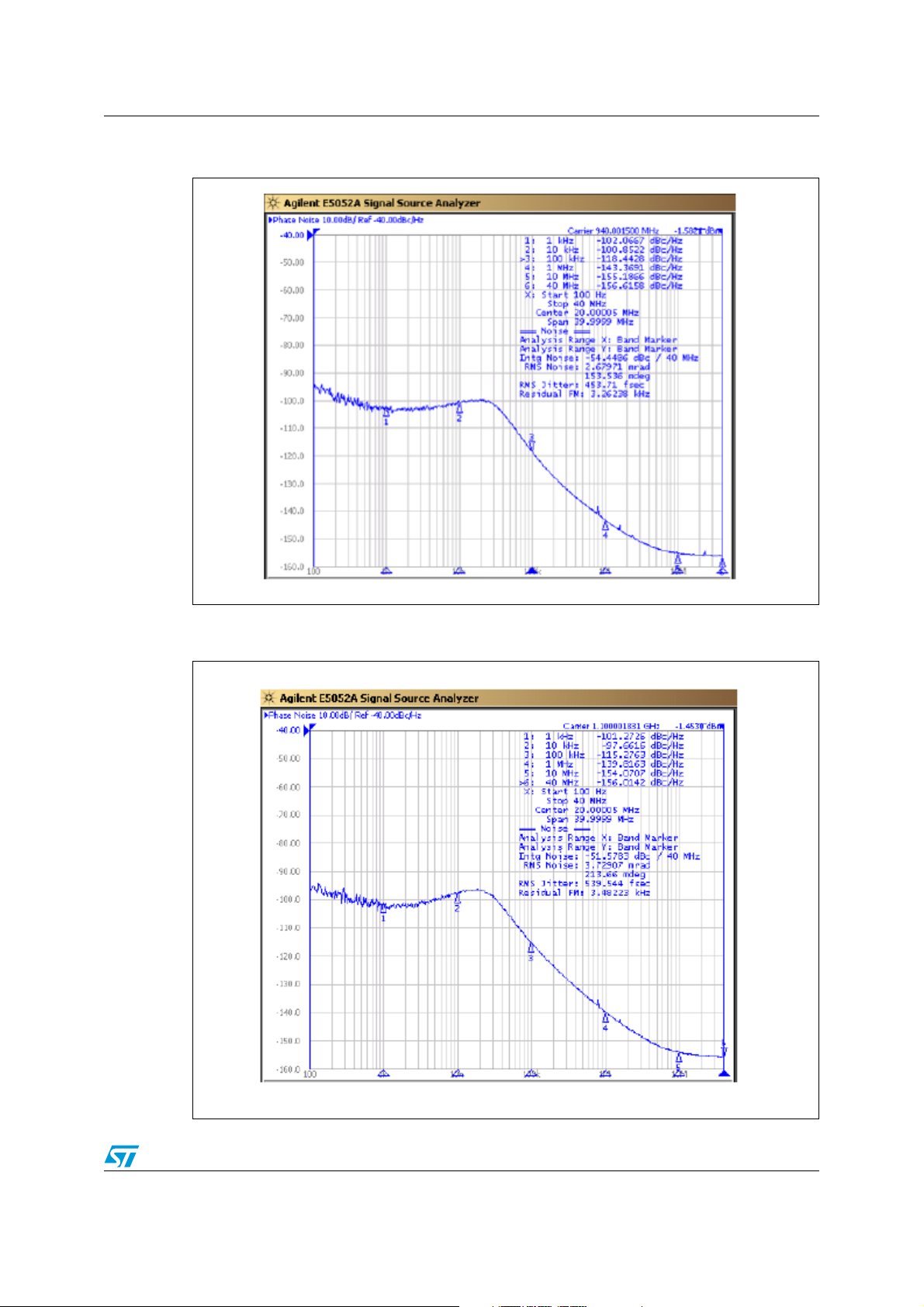
Figure 7. LOA (VCOA div. by 4) closed-loop phase noise at 0.94 GHz (F
200 kHz, I
= 1.5 mA)
CP
STEP
=
Figure 8. LOB (VCOB div. by 4) closed-loop phase noise at 1.1 GHz (F
200 kHz, I
= 1.5 mA)
CP
STEP
=
Doc ID 018503 Rev 3 23/68
Page 24
General description STW82101B
8 General description
The STW82101B (see Figure 1: STW82101B block diagram on page 7) consists of a high
linearity passive CMOS mixer with integrated RF balun, an IF amplifier, a 10-bit current
steering DAC with dual output, and an integrated integer-N synthesizer.
The synthesizer embeds 2 internal low-noise VCOs with buffer blocks, a divider by 4, a low
noise PFD (Phase Frequency Detector), a precise charge pump, a 10-bit programmable
reference divider, two programmable counters and a dual-modulus prescaler. The A-counter
(5 bits) and B counter (12 bits) counters, in conjunction with the dual modulus prescaler
P/P+1 (16/17 or 19/20), implement an N integer divider, where N = B*P+A.
The device is controlled through a digital interface (I2C bus interface or SPI digital interface).
All internal devices operate with a power supply of 3.3 V except for the IF Amplifier output
stage and the mixer driver stage operating at 5 V power supply in order to maximize the
linearity performance. If the application requires a reduced linearity and noise figure
performance the device is programmed in a low-current mode by using the minimum LO
amplitude and the minimum biasing current in the IF amplifier. In low-current mode
operation the device can use only the 3.3 V power supply thus dissipating less power.
8.1 Circuit description
8.1.1 Reference input stage
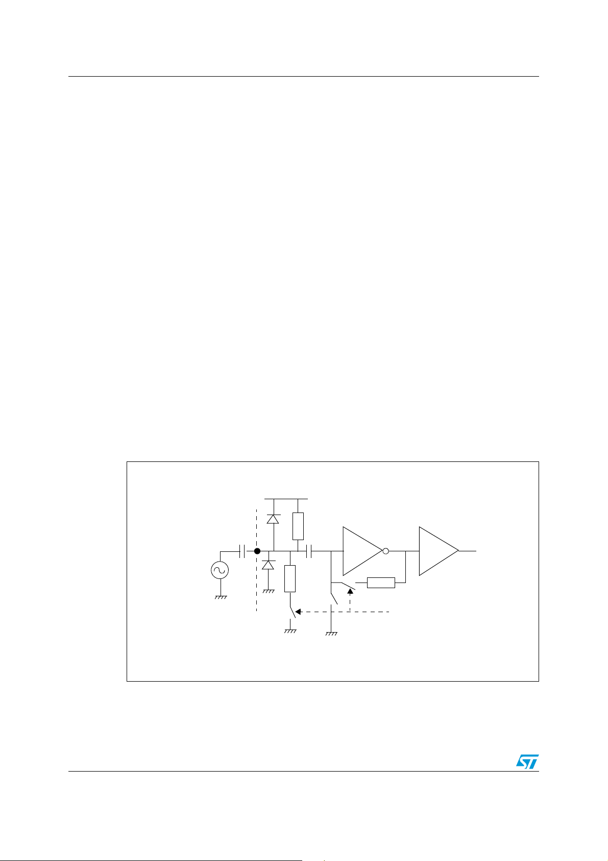
The reference input stage is shown in Figure 9. The resistor network feeds a DC bias at the
F
input while the inverter used as the frequency reference buffer is AC coupled.
ref
Figure 9. Reference frequency input buffer
F
ref
VDD
Inverter
Buffer
Power Down
24/68 Doc ID 018503 Rev 3
Page 25

STW82101B General description
8.1.2 Reference divider
The 10-bit programmable reference counter allows the input reference frequency to be
divided to produce the input clock to the PFD. The division ratio is programmed through the
digital interface.
8.1.3 Prescaler
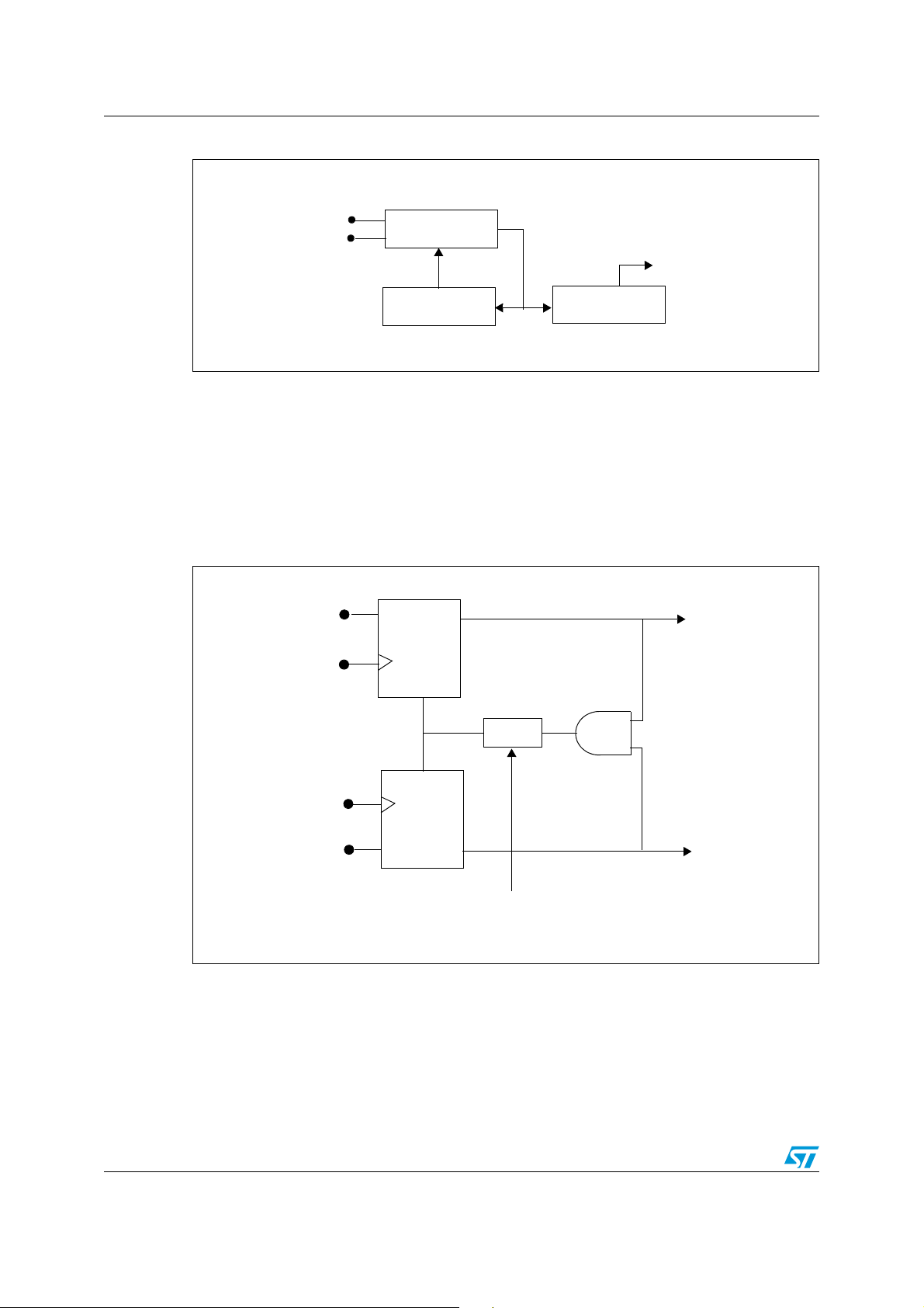
The dual-modulus prescaler P/P+1 takes the CML clock from the VCO buffer and divides it
down to a manageable frequency for the CMOS A and B counters. The modulus (P) is
programmable and can be set to 16 or 19. It is based on a synchronous 4/5 core which
division ratio depends on the state of the modulus input.
8.1.4 A and B counters
The A (5 bits) and B (12 bits) counters, in conjunction with the selected dual modulus (16/17
or 19/20) prescaler make it possible to generate output frequencies which are spaced only
by the reference frequency divided by the reference division ratio. Thus, the division ratio
and the VCO output frequency are given by the following formulae:
NBPA+×=
F
VCO
BPA+×()F
-----------------------------------------------=
×
ref
R
where:
F
: VCO output frequency.
VCO
P: modulus of dual modulus prescaler (16 or 19 selected through the digital interface).
B: division ratio of the main counter.
A: division ratio of the swallow counter.
F
: input reference frequency.
ref
R: division ratio of the reference counter.
N: division ratio of the PLL
The following points should be noted:
● For the VCO divider to work correctly, B must be higher than A.
● A can take any value from 0 to 31.
● Two PLL division ratio (N) ranges are possible, depending on the value of P:
– 256 to 65551 (when P=16)
– 361 to 77836 (when P=19).
Doc ID 018503 Rev 3 25/68
Page 26
General description STW82101B
Figure 10. VCO divider diagram
VCOBUF-
VCOBUF+
Prescaler
16/17 or 19/20
modulus
5-bit
A counter
8.1.5 Phase frequency detector (PFD)
The PFD takes inputs from the reference and the VCO dividers and produces an output
proportional to the phase error. The PFD includes a delay gate that controls the width of the
anti-backlash pulse. This pulse ensures that there is no dead zone in the PFD transfer
function.
Figure 11 is a simplified schematic of the PFD.
Figure 11. PFD diagram
VDD
F
ref_DIV
D
Q
R
To P F D
12-bit
B counter
Up
Delay
R
F
VCO_div
VDD
D
Q
ABL
26/68 Doc ID 018503 Rev 3
Down
Page 27
STW82101B General description
8.1.6 Lock detect
This signal indicates that the difference between rising edges of both UP and DOWN PFD
signals is found to be shorter than the fixed delay (roughly 5 ns). The Lock Detect signal is
high when the PLL is locked. The Lock Detector consumes current only during PLL
transients.
8.1.7 Mute until lock
This (software controlled) function shuts down the following elements until the PLL achieves
the lock status:
● RF output stage
● LO output buffer
● mixer
● IF amplifier circuitry
Under this setting there is no signal at the IF output stage or the LO output during a
frequency jump.
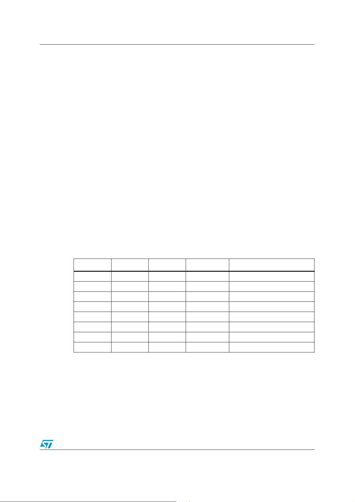
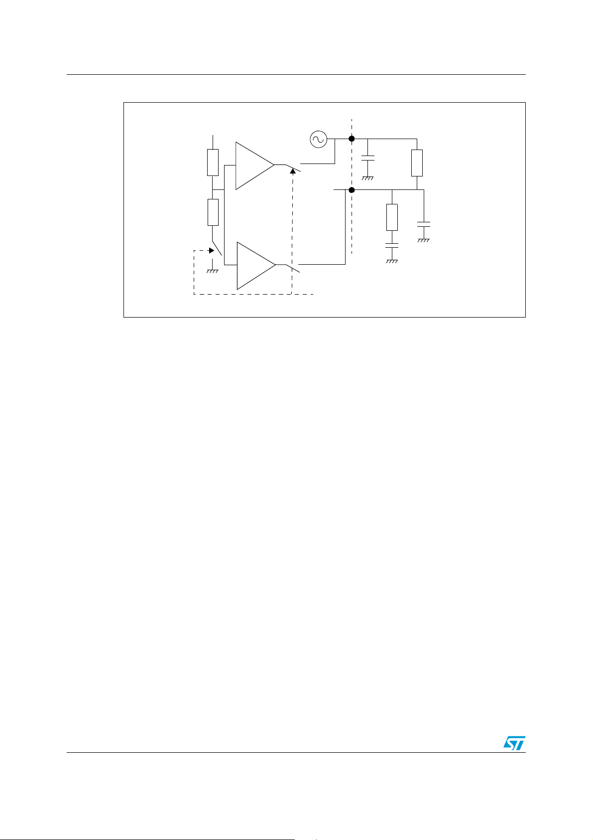
8.1.8 Charge pump
This block drives two matched current sources, Iup and Idown, which are controlled
respectively by the UP and DOWN PFD outputs. The nominal value of the output current is
controlled by an external resistor (to be connected to the REXT input pin) and the selection
of one of 8 possible values by a 3-bit word.
The minimum value of the output current is: IMIN = 2*VBG/REXT_CP (VBG~1.17 V)
Table 10. Current values for CPSEL[2:0] selection
CPSEL2 CPSEL1 CPSEL0 Current Value for REXT=4.7 kΩ
000I
0012*I
0103*I
0114*I
1005*I
1016*I
1107*I
1118*I
MIN
MIN
MIN
MIN
MIN
MIN
MIN
MIN
0.5 mA
1.00 mA
1.50 mA
2.00 mA
2.50 mA
3.00 mA
3.50 mA
4.00 mA
Note: The current is output on pin ICP. During the VCO auto calibration, ICP and VCTRL pins are
forced to VDD/2.
Doc ID 018503 Rev 3 27/68
Page 28
General description STW82101B
Figure 12. Loop filter connection
VDD
Buffer
Buffer
8.1.9 Voltage controlled oscillators
VCO selection
Within the STW82101B two low-noise VCOs are integrated to cover a wide band from
850 MHz to 1025 MHz, and from 1025 MHz to 1185 MHz after the division by 4:
● VCO A frequency range is 3400 MHz to 4100 MHz
● VCO B frequency range is 4100 MHz to 4740 MHz
Charge
pump
Cal bit
VCTRL
ICP
C3
R3
R1
C2
C1
VCO frequency calibration
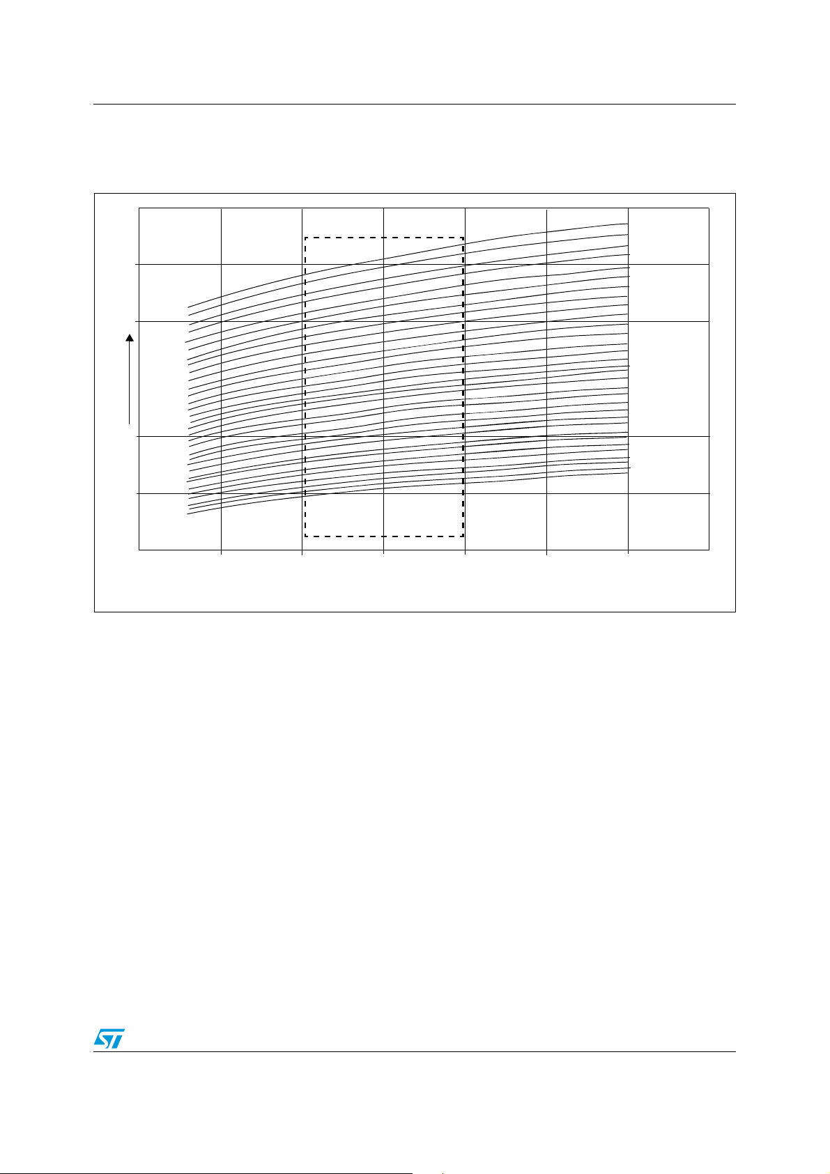
Both VCOs can operate on 32 frequency ranges that are selected by adding or subtracting
capacitors to the resonator. These frequency ranges are intended to cover the wide band of
operation and compensate for process variations on the VCO center frequency.
An automatic range selection is performed when the bit SERCAL rises from ‘0’ to ‘1’ . The
charge pump is inhibited and the pins ICP and VCTRL are set at a fixed calibration voltage
(VCAL). The frequency ranges are then tested to select the nearest one to the desired
output frequency (F
charge pump is once again enabled and the PLL performs a fine adjustment around VCAL
on the loop filter voltage to lock F
Two calibration algorithms are selectable by setting the CALTYPE bit.
Setting the CALTYPE bit to ‘1’ guarantees the PLL lock versus temperature variations. Once
programmed at the initial temperature, T
+85 °C), the synthesizer is able to maintain the lock status if the temperature drift (in either
direction) is within the limit specified by ΔT
still inside the nominal range.
Setting the CALTYPE bit to ‘0’ fixes VCAL to the mid point of the charge pump output
(VDD/2). Optimum PLL phase noise performance versus temperature variations with a
reduced ΔT
i
s guaranteed in this case.
LK
OUT
= N*F
/R) with VCAL input voltage applied. After this selection, the
ref
, thus enabling a fast settling time.
OUT
, within the operating temperature range (-40 °C to
0
, and provided that the final temperature, T
LK
1
, is
28/68 Doc ID 018503 Rev 3
Page 29
STW82101B General description
The ΔT
parameter, specific to each VCO and calibration type, in the STW82101B is
LK
specified in Table 8: Integer-N synthesizer electrical characteristics.
Figure 13. VCO typical sub-band characteristics
FREQ (Hz)
Calibrator lock
range
00000
00001
01111
11111
0.00
0.50
1.00
1.50
VCTRL (V)
2.00
2.50
3.00
3.50
The SERCAL bit should be set to ’1’ at each division ratio change. The calibration takes
approximately 7 periods of the Comparison Frequency and the SERCAL bit is automatically
reset to ’0’ at the end of each calibration.
The maximum allowed F
to perform the calibration process is 1 MHz. If a higher F
PFD
PFD
is
used the following procedure should be adopted:
1. Calibrate the VCO at the desired frequency with an F
2. Set the A, B and R dividers ratio for the desired F
PFD
lower than 1 MHz
PFD
For calibration details refer to Section 9.4.1: VCO calibration procedure (I2C interface) or
Section 10.4.1: VCO calibration procedure (SPI interface).
Doc ID 018503 Rev 3 29/68
Page 30

General description STW82101B
VCO calibration auto-restart feature
The VCO Calibration Auto-Restart feature, once activated, allows the calibration procedure
to be restarted when the Lock Detector reports that the PLL has moved to an unlock
condition (trigger on ‘1’ to ‘0’ transition of Lock Detector signal).
This situation could happen if the device experiences a significant temperature variation and
the CALTYPE bit is set for optimum PLL phase noise performance (CALTYPE [0]).
By enabling the VCO Calibration Auto-Restart feature (through the AUTO_CAL bit), the
device re-selects the proper VCO frequency sub-range, without any external user
command.
This feature can be enabled only when the F
is lower than 1 MHz.
PFD
VCO voltage amplitude control
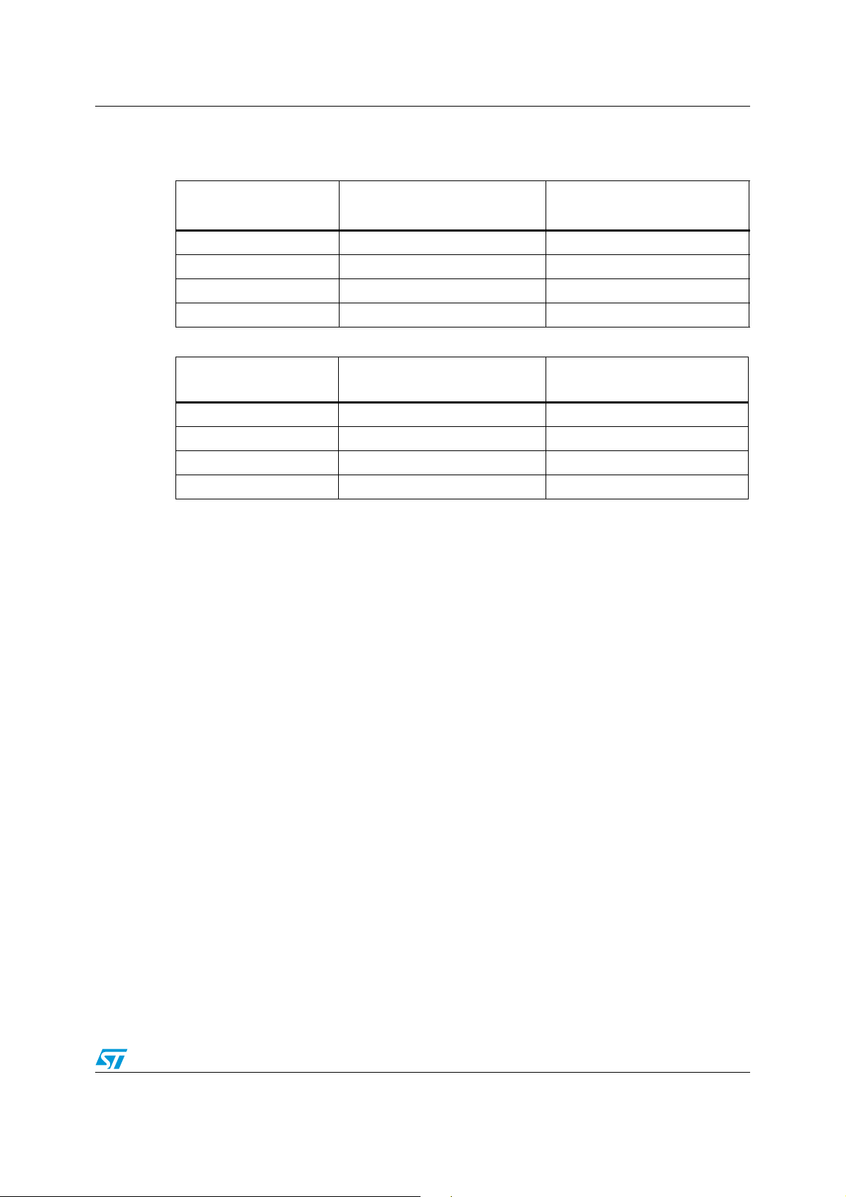
The voltage swing of the VCOs can be adjusted over 4 levels by means of two dedicated
programming bits (PLL_A1 and PLL_A0). This setting trades current consumption with
phase noise performances of the VCO. Higher amplitudes provide best phase noise while
lower ones save power.
30/68 Doc ID 018503 Rev 3
Page 31
STW82101B General description
Ta bl e 1 1 and Ta bl e 1 2 give the current consumption and the phase noise at 1 MHz.
Table 11. VCOA performance against amplitude setting (frequency = 3.6 GHz)
PLL_A[1:0]
00 23 -127
01 24 -128
10 32 -131
11 35 -132
Table 12. VCOB performance against amplitude setting (frequency = 4.3 GHz)
PLL_A[1:0]
00 16 -124
01 18 -126
10 27 -128
11 30 -129
8.1.10 Output stage
The differential output signal of the synthesizer after the Divider by 4 is available on
pins 16 and 17.
The output stage is selected by programming the PD[4:0] bits.
Current
consumption (mA)
Current
consumption (mA)
PN @ 1 MHz
PN @ 1 MHz
The output stage is an open-collector structure which is able to meet different requirements
over the desired output frequency range by proper connections on the PCB. See Figure 27:
Diversity mode operation with same LO frequencies.
8.1.11 External VCO buffer
Although the STW82101B includes two wideband and low-noise VCOs, external VCO use
capability is also provided.
The external VCO buffer can be used to manage a signal coming from an external VCO in
order to build a local oscillator signal by using the STW82101B internal synthesizer as a
PLL. This is only possible when External VCO standard mode or External VCO diversity
master mode operation are selected. See Figure 29: External VCO standard mode
operation and Figure 30: External VCO diversity mode operation with same LO.
If the STW82101B is operated in Diversity slave mode, the external VCO buffer manage the
signal coming from the synthesizer output stage of another STW82101B device See
Figure 27: Diversity mode operation with same LO frequencies and Figure 30: External
VCO diversity mode operation with same LO.
The selection of the external VCO buffer is done by setting the PD[4:0] bits.
The external VCO signal can range from 850 MHz to 1185 MHz and its minimum power
level must be -10 dBm.
Doc ID 018503 Rev 3 31/68
Page 32
General description STW82101B
8.1.12 Mixer and IF amplifier
LO mixer driver
The LO signal is fed through a driver in order to achieve the high power level needed to drive
the passive mixer for maximum performance of linearity and NF.
The LO Mixer Driver is coupled to the mixer with an integrated LO balun. The LO signal level
is adjusted by means of an Automatic Level Control loop (ALC) controlled by the bits
LO_A[1:0].
In low current mode the configuration LO_A[1:0]=’00’ (minimum LO amplitude) should be
selected and the power supply on pin 40 can be set to 3.3 V.
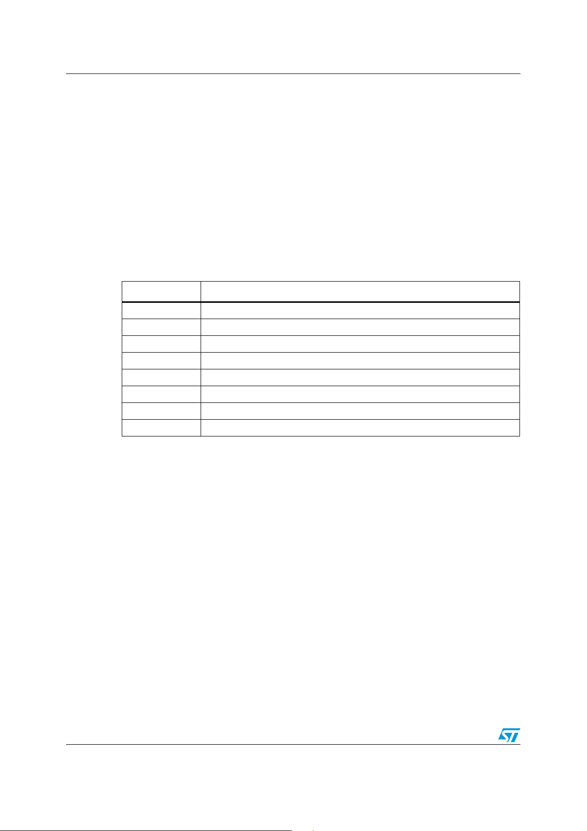
The LO balun resonating frequency can be adjusted by means of the bits CAP[2:0] in order
to match the selected LO frequency.
Suggested CAP[2:0] values for LO Frequency range mixer
CAP[2:0] LO frequency range
000 1120MHz ÷ 1185MHz
001 1065MHz ÷ 1120MHz
010 1020MHz ÷ 1065MHz
011 975MHz ÷ 1020MHz
100 940MHz ÷ 975MHz
101 905MHz ÷ 940MHz
110 875MHz ÷ 905MHz
111 850MHz ÷ 875MHz
Mixer
A doubly balanced CMOS passive mixer is internally driven by the high level LO signal in
order to achieve high linearity and low noise performance.
The RF integrated balun permits the removal of external components and it is internally
matched to 50 ohms.
The gate bias of the CMOS devices in the mixer is programmable with 4 bits (MIX[3:0]) to
optimize the input matching and the gain of the signal chain.
Higher values of gate bias (higher decimal values of MIX[3:0]) are suggested to maximize
linearity and lower values to maximize the performance of Gain and NF.
32/68 Doc ID 018503 Rev 3
Page 33
STW82101B General description
IF amplifier
The integrated IF stage permits a 200-ohm load to be driven (typically a SAW filter) ensuring
high linearity.
It is an open collector stage (pin 31, 32) and should be biased to 5 V with choke inductors.
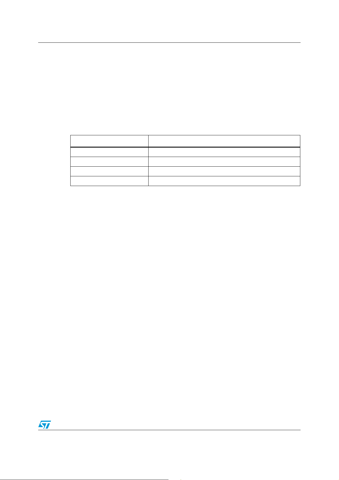
The typical output impedance is 200 ohms. The linearity performances are controlled by the
bits IFAMP[1:0]. In low current mode the configuration IFAMP[1:0]=’00’ (minimum linearity)
should be selected and the open collector stage can be biased to 3.3 V with choke
inductors.
Table 13. Linearity performance against IFAMP[1:0] configuration (typical
condition)
IFAMP[1:0] Linearity performance
00 18.5 dB
01 20.5 dB
10 22.5dB
11 24.5dB
8.1.13 Dual output current DAC
The STW82101B embeds a 10-bit Dual Output steering current DAC especially suited to
drive an external PIN diode attenuator. This provides power level calibration capability at the
RF input for the TX observation path applications.
The current sourced by the DAC is related to the R
following formulae (where VR
IDAC
LSB
IDAC
FS
With a 10 kΩ R
EXT_DAC
the FS current is approximately 2.8 mA.
EXT_DAC
1
-- -
2
1
-- -
2
is approximately 1.19 V):
3VR
×
EXT_DAC
----------------------------------------
R
EXT_DAC
3VR
×
EXT_DAC
----------------------------------------
R
EXT_DAC
××= LSB DAC current
1023
------------ -
××= Full scale current
EXT_DAC
1
------
64
64
resistor according to the
Doc ID 018503 Rev 3 33/68
Page 34
I2C bus interface STW82101B
9 I2C bus interface
The I2C bus interface is selected by hardware connection of the pin 25 (DBUS_SEL) to 0 V.
Data transmission from a microprocessor to the STW82101B takes place through the 2
wires (SDA and SCL) I
2
The I
C-bus protocol defines any device that sends data on to the bus as a transmitter and
2
C-bus interface. The STW82101B is always a slave device.
any device that reads the data as receiver. The device that controls the data transfer is
known as the master and the others as slaves. The master always initiates the transfer and
provides the serial clock for synchronization.
The STW82101B I
2
C bus supports Fast Mode operation (clock frequency up to 1 MHz).
9.1 I2C general features
9.1.1 Data validity
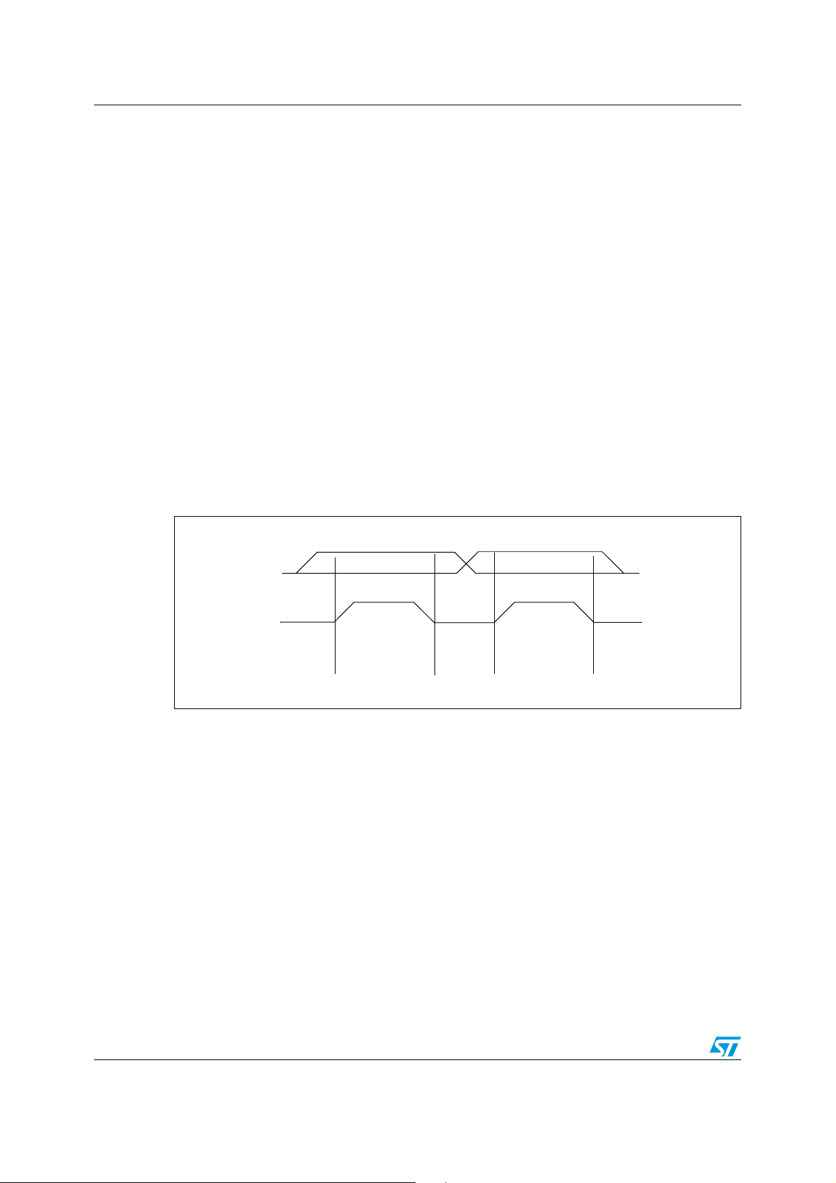
Data changes on the SDA line must only occur when the SCL is LOW. SDA transitions while
the clock is HIGH identify START or STOP conditions.
Figure 14. Data validity waveform
SDA
SCL
Data line stable
data valid
Change
data allowed
34/68 Doc ID 018503 Rev 3
Page 35
STW82101B I2C bus interface
9.1.2 START and STOP conditions
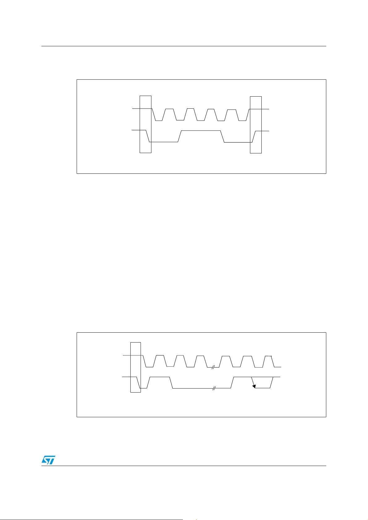
Figure 15. START and STOP condition waveform
SCL
SDA
START
START condition
A START condition is identified by a HIGH to LOW transition of the data bus SDA while the
clock signal SCL is stable in the HIGH state. A Start condition must precede any command
for data transfer.
STOP condition
A STOP condition is identified by a transition of the data bus SDA from LOW to HIGH while
the clock signal SCL is stable in the HIGH state.. A STOP condition terminates
communications between the STW82101B and the Bus Master.
9.1.3 Byte format and acknowledge
Every byte (8 bits long) transferred on the SDA line must contain bits. Each byte must be
followed by an acknowledge bit. The MSB is transferred first.
An acknowledge bit indicates a successful data transfer. The transmitter, either master or
slave, releases the SDA bus after sending 8 bits of data. During the 9th clock pulse the
receiver pulls the SDA low to acknowledge the receipt of 8 bits of data.
Figure 16. Byte format and acknowledge waveform
STOP
SCL
SDA
START
MSB
1
2
3
7
8
Acknowledgement
from receiver
STOP
9
Doc ID 018503 Rev 3 35/68
Page 36
I2C bus interface STW82101B
9.1.4 Device addressing
To start the communication between the Master and the STW82101B, the master must
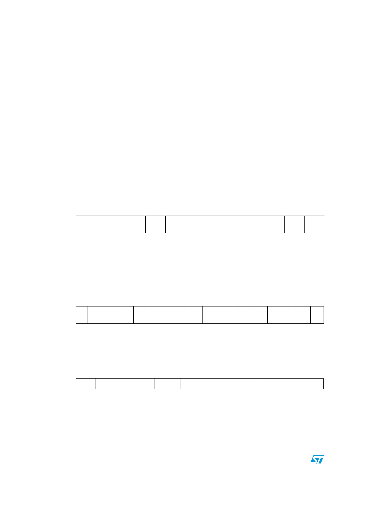
initiate with a START condition. Following this, the master sends onto the SDA line 8 bits
(MSB first) corresponding to the device select address and read or write mode.
The first 7 MSBs are the device address identifier, corresponding to the I
For the STW82101B the address is set as ’1101A
’, 3-bits programmable. The 8th bit
2A1A0
2
C-Bus definition.
(LSB) is the read or write operation bit (the RW bit is set to ‘1’ in read mode and to 0 in write
mode).
After a START condition the STW82101B identifies the device address on the bus and, if
matched, it acknowledge the identification on SDA bus during the 9th clock pulse.
9.1.5 Single-byte write mode
Following a START condition the master sends a device select code with the RW bit set to 0.
The STW82101B gives an acknowledge and waits for the internal sub-address (1 byte). This
byte provides access to any of the internal registers.
After reception of the internal byte sub-address the STW82101B again responds with an
acknowledge. A single-byte write to sub-address 0x00 would affect DATA_OUT[47:40], a
single-byte write with sub-address 0x04 would affect DATA_OUT[15:8] and so on.
S 1101A2A1A
0
0ack
9.1.6 Multi-byte write mode
The multi-byte write mode can start from any internal address. The master sends the data
bytes and each one is acknowledged. The master terminates the transfer by generating a
STOP condition.
The sub-address determines the starting byte. For example, a multi-byte write with subaddress 0x01 and 4 DATA_IN bytes affects 4 bytes starting at address 0x01 (registers at
addresses 0x01, 0x02, 0x03 and 0x04 are modified).
S 1101A2A1A00ack
sub-address
byte
9.1.7 Current byte address read
In the current byte address read mode, following a START condition, the master sends the
device address with the RW bit set to ‘1’ (No sub-address is needed as there is only 1 byte
read register). The STW82101B acknowledges this and outputs the data byte. The master
does not acknowledge the received byte, but terminates the transfer with a STOP condition.
S 1101A2A1A
0
sub-address
byte
ack DATA IN ack ..
1 ack DATA OUT No ack P
ack DATA IN ack P
DATA
IN
ack P
36/68 Doc ID 018503 Rev 3
Page 37
STW82101B I2C bus interface
9.2 I2C timing specifications
9.2.1 Data and clock timing specification
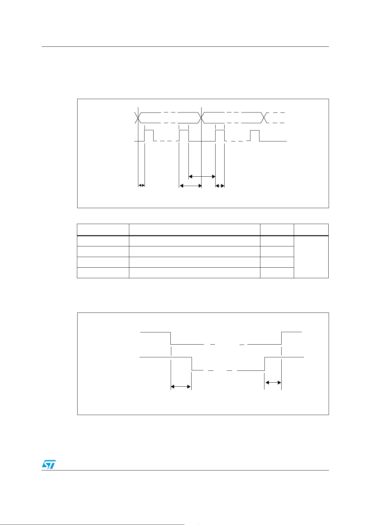
Figure 17. I2C data and clock waveforms
SDA
SCL
t
cwl
Table 14. I
t
cs
2
C data and clock timing parameters
t
ch
t
cwh
Symbol Parameter Min Unit
T
cs
T
ch
T
cwh
T
cwl
Data to clock set up time 2
Data to clock hold time 2
Clock pulse width high 10
Clock pulse width low 5.5
9.2.2 I2C START and STOP timing specification
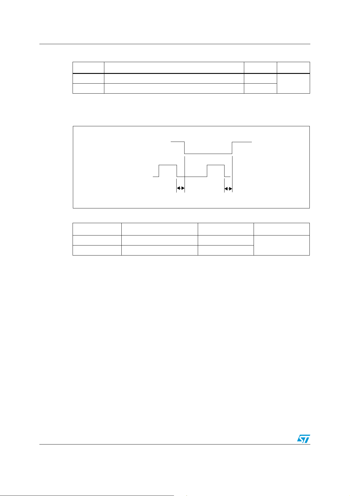
Figure 18. I2C START and STOP timing waveforms
SDA
SCL
ns
t
t
start
stop
Doc ID 018503 Rev 3 37/68
Page 38
I2C bus interface STW82101B
Table 15. I2C START and STOP timing parameters
Symbol Parameter Min Unit
T
T
start
stop
Clock to data start time 2
ns
Data to clock down stop time 2
9.2.3 I2C acknowledge timing specification
Figure 19. I2C acknowledge timing waveforms
SDA
SCL
Table 16. I2C acknowledge timing parameters
8
t
d1
9
t
d2
Symbol Parameter Max Unit
T
d1
T
d2
Ack begin delay 2
Ack end delay 2
ns
38/68 Doc ID 018503 Rev 3
Page 39
STW82101B I2C bus interface
9.3 I2C registers
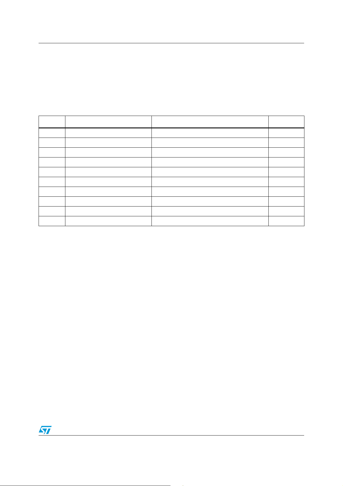
STW82101B has 9 write-only registers and 1 read-only register.
9.3.1 I2C register summary
The following table gives a short description of the write-only registers list.
Table 17. I2C register list
Offset Register name Description Page
0x00 FUNCTIONAL_MODE Functional mode register on page 40
0x01 B_COUNTER B counter register on page 40
0x02 A_COUNTER A counter register on page 41
0x03 REF_DIVIDER Reference clock divider ratio register on page 41
0x04 CONTROL PLL control register on page 42
0x05 MUTE_&_CALIBRATION Mute and calibration control register on page 43
0x06 DAC_CONTROL DAC control register on page 43
0x07 MIXER_CONTROL Mixer control register on page 44
0x08 IFAMP_LO_CONTROL IF amplifier LO control register on page 44
0x09 READ_ONLY_REGISTER Device ID and calibration status register on page 45
Doc ID 018503 Rev 3 39/68
Page 40
I2C bus interface STW82101B
9.3.2 I2C register definitions
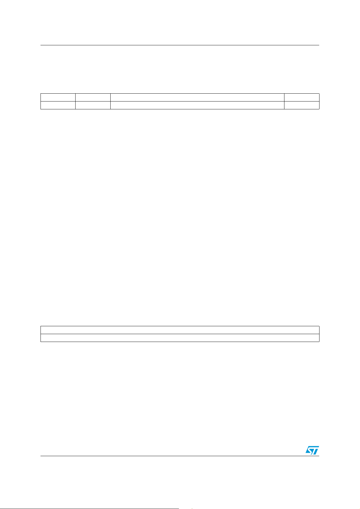
FUNCTIONAL_MODE Functional mode register
76543210
ALC_PD PKD_EN PD[4:0] B11
WWWW
Address: 0x00
Type: W
Reset: 0x00
[7] ALC_PD: for test purpose only must be set to ’0’. (ALC ON)
[6] PKD_EN: for test purpose only must be set to ’0’. (Peak detector output on pin 36 OFF)
[5:1] PD[4:0]: bits used to select different functional modes for the STW82101B according to
the following table
00000: (0 decimal) Power down mode
00001: (1 decimal) Standard Mode VCOA (VCOA and RX chain ON)
00010: (2 decimal) Standard Mode VCOB (VCOB and RX chain ON)
00011: (3 decimal). Diversity Slave Mode (ExtVCO/LO input buffer and RX Chain ON;
internal synthesizer OFF)
00100: (4 decimal) Diversity Master Mode VCOA (VCOA, RX Chain and LO output
buffer ON)
00101: (5 decimal) Diversity Master Mode VCOB (VCOB, RX Chain and LO output
buffer ON)
00110: (6 decimal) External LO Standard Mode (RX Chain ON; PLL and ExtVCO/LO
input buffer ON)
00111: (7 decimal) External LO Diversity Master Mode (RX Chain ON; PLL, ExtVCO/LO
input buffer and LO output buffer ON)
[0] B11: B counter value (bits B[10:0] in the B_COUNTER and A_COUNTER registers)
B_COUNTER B counter register
76543210
B[10:3]
W
Address: 0x01
Type: W
Reset: 0x00
Description: Most significant bits of the B counter value
[7:0] B[10:3]: B counter value (bit B11 in the FUNCTIONAL_MODE register, bits B[2:0] in the
A_COUNTER register)
40/68 Doc ID 018503 Rev 3
Page 41

STW82101B I2C bus interface
A_COUNTER A counter register
76543210
B[2:0] A[4:0]
W W
Address: 0x02
Type: W
Reset: 0x00
Description: Least significant bits of the B-counter value. A-counter value.
[7:5] B[2:0]: B Counter value (bit B11 in the FUNCTIONAL_MODE register, bits B[10:3] in
the B_COUNTER register).
[4:0] A[4:0]: A counter value
REF_DIVIDER Reference clock divider ratio register
76543210
R[9:2]
W
Address: 0x03
Type: W
Reset: 0x00
Description: Most significant bits of the reference clock divider ratio value.
[7:0] R[9:2]: Reference clock divider ratio (bits R[1:0] in the CONTROL register)
Doc ID 018503 Rev 3 41/68
Page 42

I2C bus interface STW82101B
CONTROL PLL control register
76543210
[R1:0] PLL_A[1:0] CPSEL[2:0] PSC_SEL
WW WW
Address: 0x04
Type: W
Reset: 0x00
Description: Least significant bits of the reference clock divider ratio value and PLL control bits.
[7:6] R[1:0]: Reference clock divider ratio (bits R[9:2] in the REF_DIVIDER register)
[5:4] PLL_A[1:0]:
[3:1] CPSEL[2:0]: Charge Pump output current
[0] PSC_SEL: Prescaler Modulus select (‘0’ for P=16, ‘1’ for P=19)
The LO output frequency is programmed by setting the proper value for A, B and R
according to the following formula
VCO amplitude
F
LO
:
F
ref
D
BPA+⋅()
⋅⋅=
R
--------- -
R
where DR equals 0.25 (VCOs output frequency divided by 4)
and P is the selected Prescaler Modulus
42/68 Doc ID 018503 Rev 3
Page 43

STW82101B I2C bus interface
MUTE_&_CALIBRATION Mute and calibration control register
76543210
CALTYPE
WWWWWWWW
SERCAL
SELEXTCAL
MUTE_EN
MUTE_TYPE
MUTE_LOOUT_EN
MUTE_MIX_EN
Address: 0x05
Type: W
Reset: 0x00
Description: For test purposes only
[7]
CALTYPE:
0: standard calibration to optimize the phase noise versus temperature
1: enhanced calibration to maximize the ΔTLK range
[6] SERCAL:
1: starts the VCO auto-calibration (automatically reset to ’0’ at the end of calibration)
[5] SELEXTCAL: test purpose only; must be set to ‘0’
[4] MUTE_EN:
0: mute function disabled
1: mute function enabled
[3] MUTE_TYPE: must be set to '1' while the mute function is enabled (mute the IF output
on Unlock state)
[2] MUTE_LOOUT_EN:
To be set to ’1’ to mute the LO output buffer
[1] MUTE_MIX_EN:
To be set to ’1’ mute the Mixer circuitry
[0] MUTE_IFAMP_EN: To be set to '1' to mute the IF amplifier circuitry
MUTE_IFAMP_EN
DAC_CONTROL DAC control register
76543210
DAC[9:2]
W
Address: 0x06
Type: W
Reset: 0x00
Description: Most significant bits of the DAC control word
[7:0] DAC[9:2]: DAC input word for DAC current control (bits DAC[1:0] in the
MIXER_CONTROL register).
Doc ID 018503 Rev 3 43/68
Page 44
I2C bus interface STW82101B
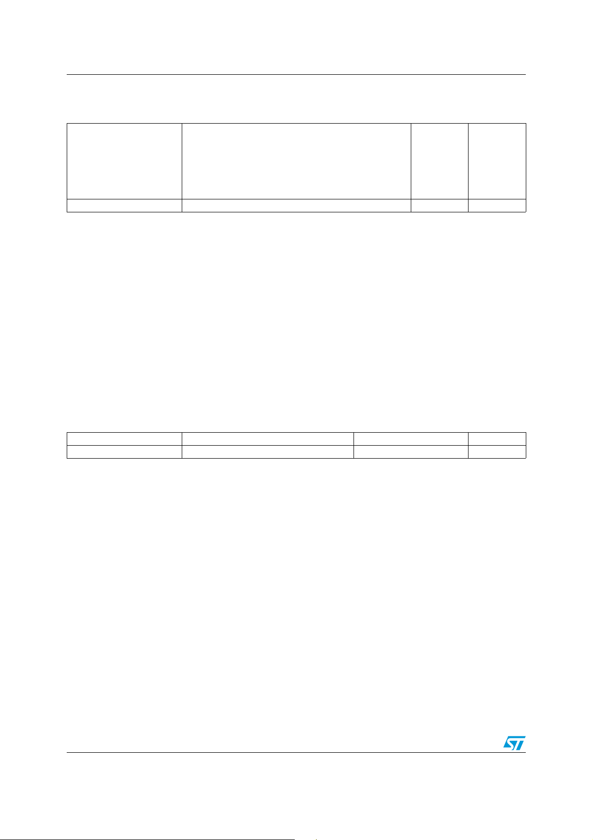
MIXER_CONTROL Mixer control register
76543210
DAC[1:0]
WWWW
MIX[3:0]
PD_DAC
Address: 0x07
Type: W
Reset: 0x00
Description: Least significant bits of DAC control word and mixer control bit fields
[7:6] DAC[1:0]: DAC input word for DAC current control (bits DAC[9:2] in the DAC_CONTROL
register)
[5:2] MIX[3:0]: Mixer bias control value
[1] PD_DAC: DAC power down
[0] CAL_AUTOSTART_EN: VCO calibration auto-restart enable (’1’ active), permits to
automatically restart the VCO calibration procedure in case of PLL unlock
IFAMP_ LO_CONTROL IF amplifier LO control register
76543210
IFAMP[1:0] CAP[2:0] LO_A[1:0] LPMUX_EN
WWWW
CAL_AUTOSTART_EN
Address: 0x08
Type: W
Reset: 0x00
[7:6] IFAMP[1:0]: power consumption/linearity control
[5:3] CAP[2:0]: Tuning capacitors control
[2:1] LO_A[1:0]: LO amplitude control
[0] LPMUX_EN: for test purpose only (low power mode for MUX); must be set to ’0’
44/68 Doc ID 018503 Rev 3
Page 45

STW82101B I2C bus interface
READ-ONLY REGISTER Device ID and calibration status register
76543210
ID[1:0] LOCK_DET INTCAL[4:0]
RR R
Address: 0x09
Type: R
Reset: 0x00
Description: This register is automatically addressed in the ‘current byte address read mode’
[7:6] ID[1:0]: device identification ’01’ for STW82101B
[5] LOCK_DET: ’1’ when PLL is locked
[4:0] INTCAL[4:0]: internal value of the VCO calibration control word
Doc ID 018503 Rev 3 45/68
Page 46

I2C bus interface STW82101B
9.4 Device calibration through the I2C interface
9.4.1 VCO calibration procedure (I2C interface)
The calibration of the VCO center frequency is activated by setting the SERCAL bit of the
MUTE & CALIBRATION register to ’1’.
To program the device ensuring a correct VCO calibration, the following procedure is
required before every channel change:
1. Program all the Registers using a multi-byte write sequence with the desired setting:
– Functional Mode
– B and A counters
– R counter
– VCO amplitude
– Charge Pump
– Prescaler Modulus
–DAC
– Mixer and LO Control
– all bits of the MUTE & CALIBRATION Register (0x05) set to ’0’.
2. Program the MUTE & CALIBRATION register using a single-byte write sequence (subaddress 0x05) with the SERCAL bit set to ’1’.
The maximum allowed PFD frequency (F
the desired F
is higher than 1 MHz the following steps are needed:
PFD
PFD
3. Perform all the step of the above calibration procedure programming the desired VCO
frequency with a proper setting of R, B and A counter so that F
1MHz.
4. Once calibration is completed, program all the Registers by using a multi-byte write
sequence (Functional Mode, B and A counters, R counter, VCO amplitude, Charge
Pump, Prescaler Modulus, DAC, Mixer and LO Control) with the proper settings for the
desired VCO and PFD frequencies.
9.4.2 Power ON sequence (I2C interface)
At power-on the device is configured in power-down mode.
In order to guarantee correct setting of the internal circuitry after the power on, the following
steps must be followed:
1. Power up the device
2. Provide the Reference clock
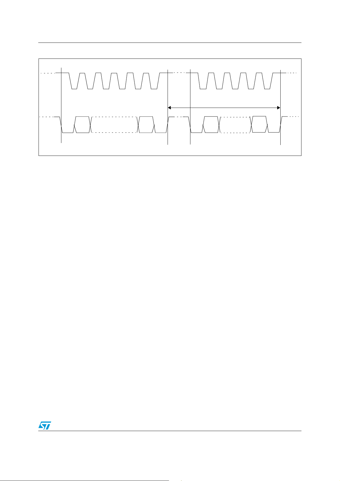
3. Implement the first programming sequence with a proper delay time between the STOP
condition of the multi-byte write sequence and that of the single-byte write sequence
(see Figure 20). The T
value must respect the following condition:
delay
T
delay
) to perform the calibration process is 1 MHz. If
results lower than
PFD
1
1023
--------- -
×>
F
ref
F
is the reference clock frequency.
ref
46/68 Doc ID 018503 Rev 3
Page 47
STW82101B I2C bus interface
Figure 20. I2C first programming timing
START
CLK
START
STOP STOP
Tdelay > 1023/F
DATA
MSB
LSB
Multi-byte sequence Single-byte sequence
MSB
9.4.3 VCO calibration auto-restart procedure (I2C interface)
The VCO calibration auto-restart feature is enabled in two steps:
1. Set the desired frequency ensuring VCO calibration procedure as described above
(Section 9.4.1).
2. Program the MIXER_CONTROL register (sub-address 0x07) using a single-byte write
sequence with the CAL_AUTOSTART_EN bit set to '1' while keeping the others
unchanged.
ref
LSB
Doc ID 018503 Rev 3 47/68
Page 48
SPI digital interface STW82101B
10 SPI digital interface
10.1 SPI general features
The SPI digital interface is selected by hardware connection of the pin 25 (DBUS_SEL) to
3.3 V.
The STW82101B IC is programmed by means of a high-speed serial-to-parallel interface
with write option only. The 3-wires bus can be clocked at a frequency as high as 100 MHz to
allow fast programming of the registers containing the data for RF IC configuration.
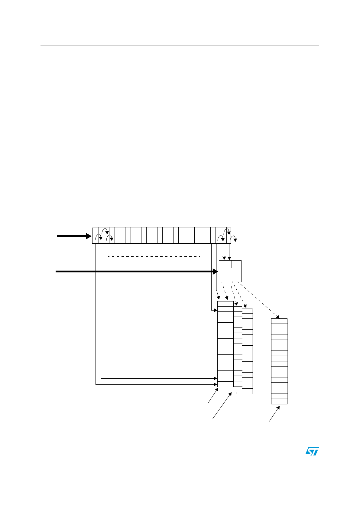
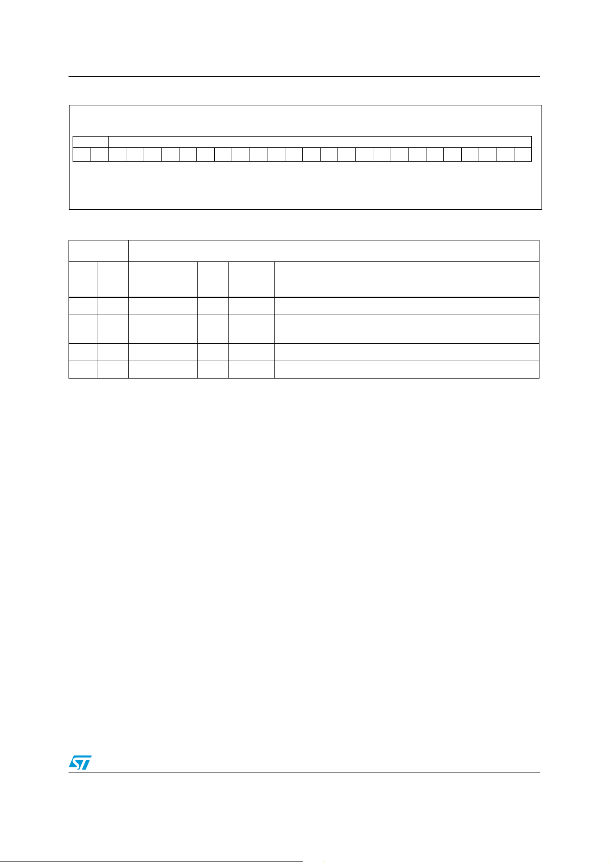
The programming of the chip is done through serial words with whole length of 26 bits. The
first 2 MSB represent the address of the registers. The others 24 LSB represent the value of
the registers.
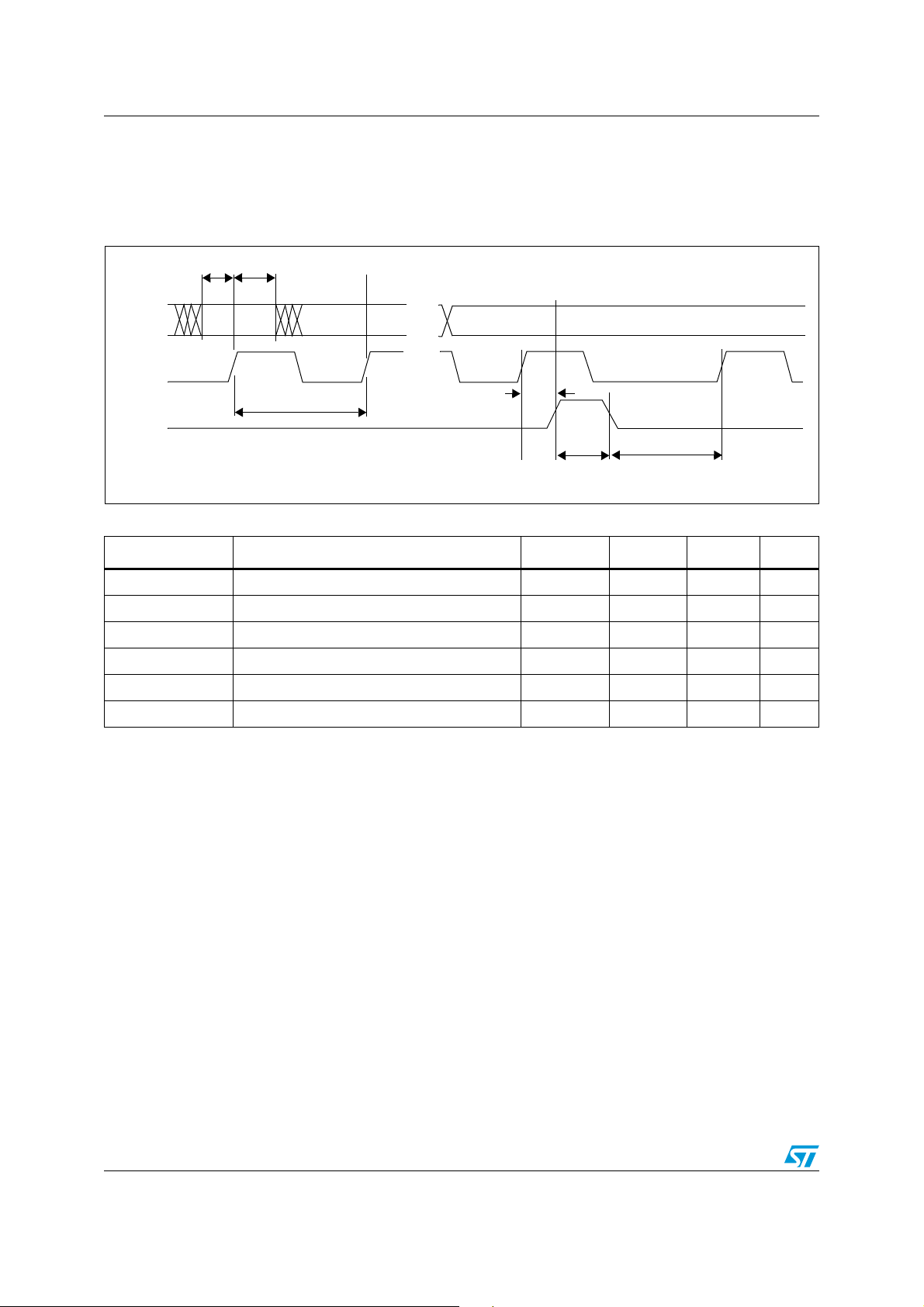
Each data bit is stored in the internal shift register on the rising edge of the CLOCK signal.
On the rising edge of the LOAD signal the outputs of the selected register are sent to the
device.
Figure 21. SPI input and output bit order
Last
DATA
bit sent
(LSB) 0
2
1
23
25 (MSB)
24
LOAD
Reg. #0
Reg. #1
A1
Address
decoder
LOAD #4
00 (LSB)
Reg. #4
48/68 Doc ID 018503 Rev 3
Page 49
STW82101B SPI digital interface
Figure 22. SPI data structure
MSB
Address
A1 A0 D23 D22 D21 D20 D19 D18 D17 D16 D15 D14 D13 D12 D11 D10 D9 D8 D7 D6 D5 D4 D3 D2 D1 D0
Table 18. Address decoder and outputs
Data for register (24 bits)
Note: MSB is sent first
Address Outputs
A1 A0
DATABITS
D23-D0
o
N
Name Function
0 0 24 0 ST1 DAC, Mixer, Tuning capacitors, LO_amplitude
01 24 1ST2
Reference divider, VCO amplitude, VCO Calibration, Charge
Pump current, Prescaler Modulus, Mute functions
1 0 24 2 ST3 Functional modes, VCO dividers
1 1 24 3 ST4 Reserved
LSB
Doc ID 018503 Rev 3 49/68
Page 50
SPI digital interface STW82101B
10.2 SPI timing specification
10.2.1 Data, clock and load timing
Figure 23. SPI timing waveforms
t
t
setup
hold
DATA
CLOCK
LOAD
Table 19. SPI timing parameters
MSB LSBMSB - 1
t
clk
t
clk_loadr
t
load
t
clk_loadf
Parameter Description Min. Typ. Max. Unit
t
setup
t
hold
t
clk
t
load
t
clk_loadr
t
clk_loadf
DATA to CLOCK setup time 1 - - ns
DATA to clock hold time 0.5 - - ns
CLOCK cycle period 10 - - ns
LOAD pulse width 3 - - ns
CLOCK to LOAD rising edge 0.6 - - ns
CLOCK to LOAD falling edge 2.5 - - ns
50/68 Doc ID 018503 Rev 3
Page 51
STW82101B SPI digital interface
10.3 SPI registers
10.3.1 SPI register summary
Table 20. SPI register list
Offset Register name Description Page
0x00 ST1 SPI register 1 on page 51
0x01 ST2 SPI register 2 on page 52
0x10 ST3 SPI register 3 on page 53
10.3.2 SPI register definitions
ST1 SPI register 1
23222120191817161514131211109876543210
Address: 0x00
Type: W
CAL_AUTOSTART_EN
IF[1:0]
CAP[2:0]
LO_A[1:0]
DAC[9:0]
WWWWWWWW
MIX[3:0]
PWD_DAC
LPMUX_EN
Reset: 0x00
[23:14]
[13:10]
[9]
[8]
[7:6]
[5:3]
[2:1]
[0]
DAC[9:0]: DAC input word
MIX[3:0]: Mixer bias control
PWD_DAC: DAC power down
CAL_AUTOSTART_EN: VCO calibration auto-restart enable
IF[1:0]: Power consumption/linearity control
CAP[2:0]: Tuning capacitors control
LO_A[1:0]: LO amplitude control
LPMUX_EN: For test purpose only. Must be set to ‘0’
Doc ID 018503 Rev 3 51/68
Page 52
SPI digital interface STW82101B
ST2 SPI register 2
23 22 21 20 19 18 17 16 15 14 13 12 11 10 9 8 7 6 5 4 3 2 1 0
R[9:0]
W W W WWWWWWWWW
PLL_A[1:0]
CPSEL[2:0]
PSC_SEL
CAL_TYPE
SERCAL
SELEXTCAL
MUTE_EN
MUTE_TYPE
MUTE_LOOUT_EN
Address: 0x01
Type: W
Reset: 0x00
[23:14]
[13:12]
R[9:0]: Reference clock divider ratio
PLL_A[1:0]: VCO amplitude control
[11:9]
CPSEL[2:0]: Charge pump output current control
[8]
PSC_SEL: Prescaler modulus select (‘0’ for P=16, ‘1’ for P=19)
[7] CAL_TYPE: Calibration algorithm selection
0: standard calibration to optimize the phase noise versus temperature
1: enhanced calibration to maximize the ΔTLK range
[6] SERCAL:
at ‘1’ starts the VCO auto-calibration (automatically reset to ‘0’ at the end of calibration)
[5]
SELEXTCAL: test purpose only. Must be set to ‘0’
MUTE_MIX_EN
MUTE_IFAMP_EN
[4] MUTE_EN:
0: mute function disabled
1: mute function enabled
[3] MUTE_TYPE: must be set to '1' while the mute function is enabled (mute IF output on
Unlock state)
[2] MUTE_LOOUT_EN:
To be set to ’1’ to mute the LO output buffer
[1] MUTE_MIX_EN:
To be set to ’1’ to mute the Mixer circuitry
[0] MUTE_IFAMP_EN:
To be set to ’1’ to mute the IF amplifier circuitry
52/68 Doc ID 018503 Rev 3
Page 53

STW82101B SPI digital interface
ST3 SPI register 3
23 22 21 20 19 18 17 16 15 14 13 12 11 10 9 8 7 6 5 4 3 2 1 0
ALC_PD
WW W W W
PKD_EN
PD[4:0]
B[11:0]
A[4:0]
Address: 0x10
Type: W
Reset: 0x00
[23]
ALC_PD: Test purpose only; must be set to ‘0’ (ALC ON)
[22] PKD_EN: for test purpose only; must be set to ‘0’
[21:17] PD[4:0]:
00000: (0 decimal) Power down mode
00001: (1 decimal) Standard Mode VCOA (VCOA and RX chain ON)
00010: (2 decimal) Standard Mode VCOB (VCOB and RX chain ON)
00011: (3 decimal). Diversity Slave Mode (ExtVCO/LO input buffer and RX Chain ON;
internal synthesizer OFF)
00100: (4 decimal) Diversity Master Mode VCOA (VCOA, RX Chain and LO output
buffer ON)
00101: (5 decimal) Diversity Master Mode VCOB (VCOB, RX Chain and LO output
buffer ON)
00110: (6 decimal) External LO Standard Mode (RX Chain ON; PLL and ExtVCO/LO
input buffer ON)
00111: (7 decimal) External LO Diversity Master Mode (RX Chain ON; PLL, ExtVCO/LO
input buffer and LO output buffer ON)
[16:5] B[11:0]: B counter bits
[4:0]
A[4:0]: A Counter Bits
Doc ID 018503 Rev 3 53/68
Page 54

SPI digital interface STW82101B
10.4 Device calibration through the SPI interface
10.4.1 VCO calibration procedure (SPI interface)
The calibration of the VCO center frequency is activated by setting to ’1’ the SERCAL bit
(ST2 Register bit [6]).
In order to program properly the device while ensuring the VCO calibration, the following
procedure is required before every channel change:
1. Program the ST1 Register with the desired setting (DAC, Mixer, LO Control)
2. Program the ST3 Register with the desired setting (Functional mode, B and A counters)
3. Program the ST2 Register with the desired setting (R counter, VCO amplitude, Charge
Pump, Prescaler Modulus) and SERCAL bit set to ’1’
The maximum allowed PFD frequency (F
the desired F
is higher than 1 MHz the following steps are needed:
PFD
PFD
4. Perform all the steps of the above calibration procedure programming the desired VCO
frequency with a proper setting of R, B and A counter so that F
MHz.
5. Once calibration is completed program the device with the proper setting for the desired
VCO and PFD frequencies according to the following steps:
a) Program the ST3 Register with the desired setting (Functional mode, B and A
counters)
b) Program the ST2 Register with the desired setting (R counter, VCO amplitude,
Charge Pump, Prescaler Modulus) with the SERCAL bit set to ’0’.
10.4.2 Power ON sequence (SPI interface)
At power-on the device is configured in power-down mode.
In order to guarantee correct setting of the internal circuitry after the power on, the following
steps must be followed:
1. Power up the device
2. Provide the reference clock
3. Implement the first programming sequence with a proper delay time between the ST3
and ST2 load rising edges (see Figure 24). The T
condition:
) to perform the calibration process is 1 MHz; if
results lower than 1
PFD
value must respect the following
delay
T
F
is the reference clock frequency.
ref
54/68 Doc ID 018503 Rev 3
delay
1023
1
--------- -
×>
F
ref
Page 55
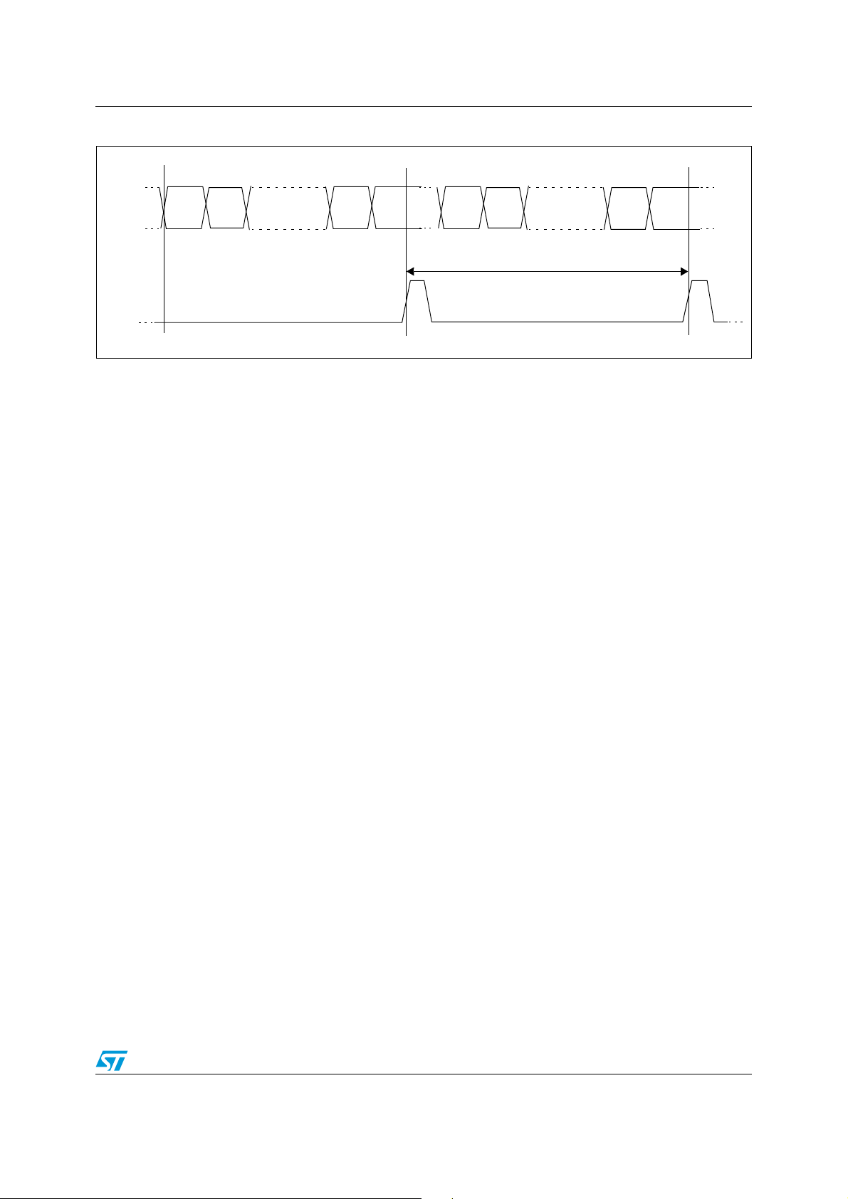
STW82101B SPI digital interface
Figure 24. SPI first programming timing
T
delay
ST2
> 1023/F
ref
DATA
LOAD
MSB MSB-1
ST3
LSB-1
LSB
MSB
MSB-1
10.4.3 VCO calibration auto-restart procedure (SPI interface)
The VCO calibration auto-restart feature is enabled in two steps:
1. Set the desired frequency ensuring VCO calibration as described in Section 10.4.1.
2. Program the ST1 register with the CAL_AUTOSTART_EN bit set to '1' while keeping
unchanged the others.
LSB-1
LSB
Doc ID 018503 Rev 3 55/68
Page 56
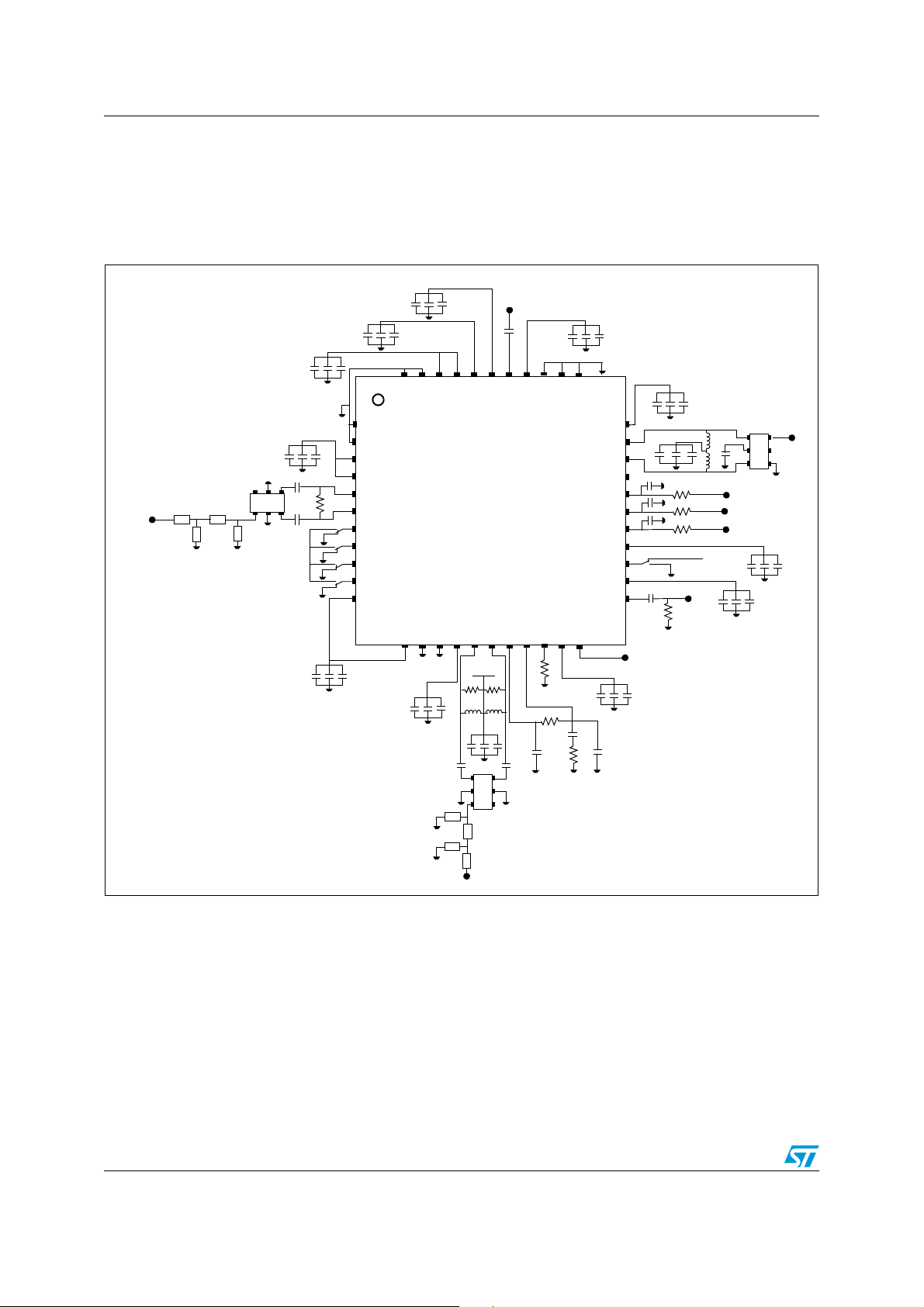
Application information STW82101B
11 Application information
11.1 Application circuit
Figure 25. Typical STW82101B application circuit
3.3V_LN4
C1
C2
External VCO
C3
5V_1
C1
C2
C3
3.3V_LN1
C1
C2
C3
42
43
44
1
3.3V_LN1
C1
C2
C3
NC
6
U1
X1
X2
1
X3
X4
C4
4
5
R1
2
3
C5
3.3V_LN1
VDD_DAC
2
REXT_DAC
3
VDD_DIV
4
VDD_VCO
5
EXTVCO_INN
6
EXTVCO_INP
EXT_PD
7
ADD2
8
ADD1
9
ADD0
10
VDD_IO
11
12
I_PINDRV2
I_PINDRV1
VDD_PSCBUF
NC
13
41
VDD_MIXDRV
VFQFPN-44
NC
14
3.3V_LN1
C1
C2
C3
C1
3.3V_LN1
C2
C3
C6
X5
X7
VDD_ALC
VDD_OUTBUF
15
C1
40
MIXDRV_CT
OUTBUFN
16
17
3.3V_LN1
R2
L1
C2
3
5
2
1
6
U2
X6
X8
LO_Output
RF_IN
C19
38
39
RF_IN
VDD_RFESD
VCTRL
OUTBUFP
18 19
R3
L2
C3
C7
4
NC
C1
C2
C3
33
32
31
NC
30
29
28
27
26
25
LOCK_DET
C2
3.3V_LN3
C1
C2
C3
U3
IF_out
5V_2
C17
R10
R9
R8
3.3V_LN2
REF_CLK
L3
L4
LOAD
SLC/CLK
SDA/DATA
3.3V_LN2
C1
C15 C16
C14
C13
C12
SPI
I2C
24
C11
23
R7
C3
C18
3.3V_LN2
C1
C2
C3
1
6
NC
5
2
4
3
C2
C3
36
37
C8
34
35
TEST1
RF_CT
ICP
R6
TEST2
TEST_ALC
VDD_IFAMP
IF_OUTP
IF_OUTN
LOAD
SLC/CLK
SDA/DATA
VDD_DIG
DBUS_SEL
VDD_PLL
REF_CLK
REXT_CP
VDD_CP
LOCK_DET
22
20
21
3.3V_LN1
C1
R4
C9
C10
R5
56/68 Doc ID 018503 Rev 3
Page 57
STW82101B Application information
Table 21. Application circuit component values
Designation Qty Description Supplier
C1, C15 2 4.7 µF capacitors COG (0402)
C2, C11 2 1 nF capacitors COG (0402)
C3, C6, C7 3 10 pF capacitor COG (0402)
C4,C5, C12, C13, C14 5 15 pF capacitors COG (0402)
C8 1 270 pF capacitor COG (0402)
C9 1 2.7 nF capacitor COG (0402)
C10 1 68 pF capacitor COG (0402)
C16 1 100 nF capacitor COG (0402)
C17 1 100 pF capacitor COG (0402)
C19 1 22 pF capacitor COG (0402)
R1,R7 2 50 ohm resistors (0402) -
R2,R3 2 25 ohm resistors (0402) -
R4 1 2.2 kohm resistor (0402) -
R5 1 8.2 kohm resistor (0402) -
R6 1 4.7 kohm resistor (0402) -
R8, R9, R10 3 100 ohm resistors (0402) -
Murata Manufacturing Co., Ltd
Murata Manufacturing Co., LtdC18 1 180 pF capacitor COG (0402)
U1, U2 2 Balun JTI - 0900BL15C050 Johanson Technology
U3 1 Balun ADT4-5WT Mini Circuits
X1 1 15 pF capacitor COG (0402)
Murata Manufacturing Co., Ltd
X2 1 1.2 pF capacitor COG (0402)
X3 1 3.3 nH inductor CS (0402) Coilcraft, Inc
X4 0 NC -
X5 0 NC -
X6 1 3.3 nH inductor CS (0402) Coilcraft, Inc
X7 1 1.2 pF capacitor COG (0402)
Murata Manufacturing Co., Ltd
X8 1 10 pF capacitor COG (0402)
L1, L2 2 11 nH inductors CS (0402)
Coilcraft, Inc
L3, L4 2 220 nH inductors CS (1206)
Note: 1 or optimum performance a low-noise 3.3 V power supply must be used.
2 The 3.3 V and 5 V power supplies are split in order to maximize the isolation between RF,
LO, IF and digital sections.
Doc ID 018503 Rev 3 57/68
Page 58
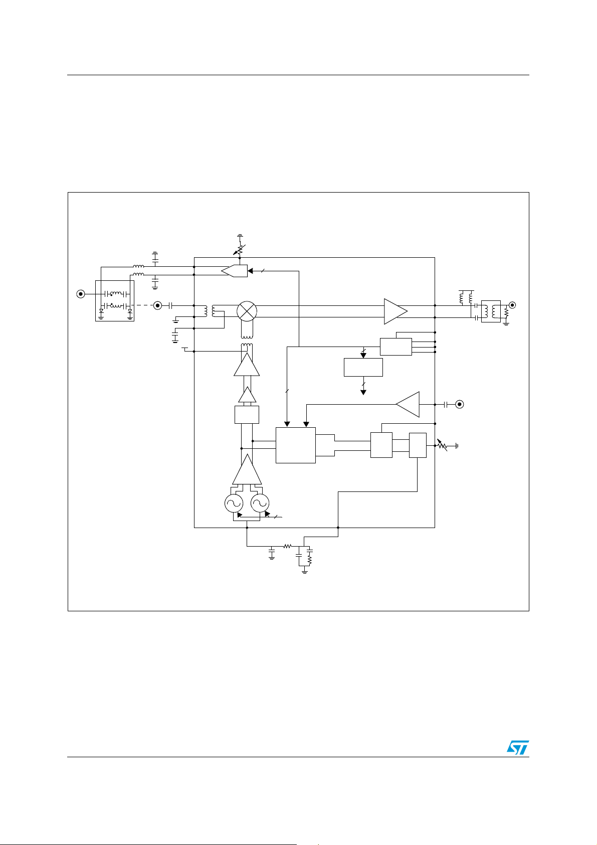
Application information STW82101B
11.2 Standard Mode Operation
The STW82101B can be used in Standard Mode for both RX path and TX observation path
(RX Chain ON and Synthesizer ON).
In such a case the 10-bit internal DAC can drive an external PIN diode attenuator in order to
calibrate the signal level at the input of the device.
Figure 26. Standard mode operation
RF_IN2
RF_IN
I_PINDRV1
I_PINDRV2
RF_IN
RF_VSS
RF_CT
5V
MIXDRV_CT
DAC
VCTRL
MIX
DRV
DIV4
VCO
BUFF
REXT_DAC
STW82101B
5V
4:1
IF_OUT
50 Ω
CAL_VCO
PLL
ICP
VCO
calibrator
CAL_VCO
PFD
IF AMP
DBUS
IF_OUTP
IF_OUTN
DBUS_SEL
SDA/DATA
SCL/CLK
LOAD
BUF
UP
DN
REF_CLK
LOCK_DET
CHP
REXT_CP
58/68 Doc ID 018503 Rev 3
Page 59
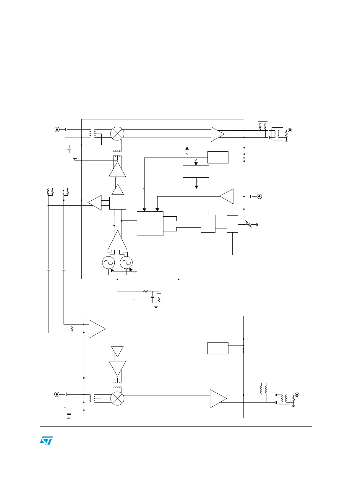
STW82101B Application information
11.3 Diversity mode operation with same LO frequency
The STW82101B supports the Diversity mode with the same LO frequency by using one
STW82101B in Master Mode (RX Chain ON, Synthesizer ON and LO output buffer ON) and
the other in Slave Mode (RX Chain ON, Synthesizer OFF and EXT VCO/LO buffer ON). This
operation mode is suitable for antenna diversity.
Figure 27. Diversity mode operation with same LO frequencies
RF_IN_M
3.3V
50 Ω
RF_IN
RF_VSS
RF_CT
5V
MIXDRV_CT
50 Ω
OUTBUFP
OUTBUFN
LO
OUT
VCTRL
MIX
DRV
DIV4
VCO
BUFF
STW82101B Master
PLL
CAL_VCO
ICP
to DAC
VCO
calibrator
CAL_VCO
PFD
IF AMP
DBUS
5V
4:1
IF_OUTP
IF_OUTN
DBUS_SEL
SDA/DATA
SCL/CLK
LOAD
BUF
UP
CHP
DN
REF_CLK
LOCK_DET
REXT_CP
IF_M
50 Ω
RF_IN_S
EXTVCO_INP
100 Ω
EXTVCO_INN
5V
MIXDRV_CT
RF_IN
RF_VSS
RF_CT
EXT
LO/VCO
BUF
MIX
DRV
STW82101B Slave
DBUS_SEL
DBUS
IF AMP
SDA/DATA
SCL/CLK
LOAD
IF_OUTP
IF_OUTN
5V
4:1
Doc ID 018503 Rev 3 59/68
IF_S
50 Ω
Page 60
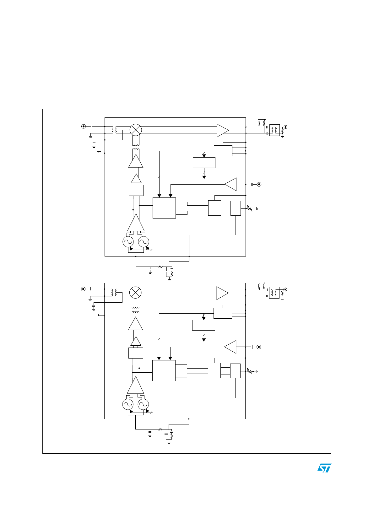
Application information STW82101B
11.4 Diversity mode operation with different LO frequencies
The STW82101B is particularly suitable for Diversity schemes using different LO
frequencies such as the Interferer Diversity. In these schemes two STW82101Bs are used,
each one set in Standard Mode and with different LO frequencies.
Figure 28. Diversity mode operation with different LO frequencies
RF_IN1
RF_IN2
RF_IN
RF_VSS
RF_CT
5V
MIXDRV_CT
RF_IN
RF_VSS
RF_CT
5V
MIXDRV_CT
VCTRL
LO1
MIX
DRV
DIV4
VCO
BUFF
LO2
MIX
DRV
DIV4
VCO
BUFF
STW82101B Master
PLL
CAL_VCO
STW82101B Diversity
PLL
ICP
VCO
calibrator
VCO
calibrator
CAL_VCO
PFD
CAL_VCO
PFD
IF AMP
DBUS
IF AMP
DBUS
5V
4:1
IF_OUTP
IF_OUTN
DBUS_SEL
SDA/DATA
SCL/CLK
LOAD
CHP
CHP
REF_CLK
LOCK_DET
REXT_CP
IF_OUTP
IF_OUTN
DBUS_SEL
SDA/DATA
SCL/CLK
LOAD
REF_CLK
LOCK_DET
REXT_CP
5V
BUF
UP
DN
BUF
UP
DN
IF_OUT1
50 Ω
4:1
IF_OUT2
50 Ω
VCTRL
CAL_VCO
ICP
60/68 Doc ID 018503 Rev 3
Page 61
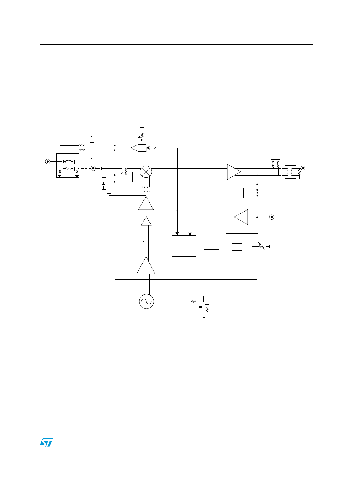
STW82101B Application information
11.5 External VCO standard mode operation
The STW82101B can be used in Ext VCO Mode for both RX path and TX observation path
(RX Chain ON, Synthesizer ON, EXT VCO/LO buffer ON and with an external VCO).
In such a case the 10-bit internal DAC can drive an external PIN diode attenuator in order to
calibrate the signal level at the input of the device.
Figure 29. External VCO standard mode operation
RF_IN2
RF_IN
I_PINDRV1
I_PINDRV2
RF_IN
RF_VSS
RF_CT
5V
MIXDRV_CT
EXTVCO_INP
EXTERNAL
VCO
DAC
LO/VCO
MIX
DRV
EXT
BUF
REXT_DAC
EXTVCO_INN
STW82101B
PLL
PFD
IF AMP
DBUS
5V
4:1
IF_OUTP
IF_OUTN
DBUS_SEL
SDA/DATA
SCL/CLK
LOAD
BUF
UP
DN
REF_CLK
LOCK_DET
CHP
REXT_CP
ICP
IF_OUT
50 Ω
Doc ID 018503 Rev 3 61/68
Page 62
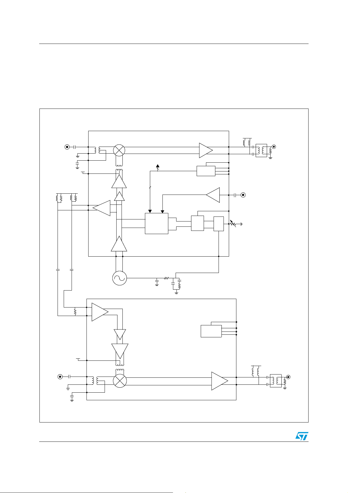
Application information STW82101B
11.6 External VCO diversity mode operation with same LO
The STW82101B can be used in Diversity mode using one STW82101B in Master Mode
(RX Chain ON, Synthesizer ON, EXT VCO/LO buffer ON, LO output buffer ON and with an
external VCO) and the other one in Slave Mode (RX Chain ON, Synthesizer OFF and EXT
VCO/LO buffer ON).
Figure 30. External VCO diversity mode operation with same LO
RF_IN_M
3.3V
50 Ω
EXTVCO_INP
100 Ω
EXTVCO_INN
RF_IN
RF_VSS
RF_CT
5V
MIXDRV_CT
50 Ω
OUTBUFP
OUTBUFN
LO/2xLO
OUT
EXTVCO_INP
EXTERNAL
VCO
EXT
LO/VCO
BUF
MIX
DRV
VCO
BUFF
EXTVCO_INN
STW82101B Master
to DAC
PLL
STW82101B Slave
PFD
IF AMP
DBUS
UP
DN
DBUS
BUF
CHP
ICP
IF_OUTP
IF_OUTN
DBUS_SEL
SDA/DATA
SCL/CLK
LOAD
REF_CLK
LOCK_DET
REXT_CP
DBUS_SEL
SDA/DATA
SCL/CLK
LOAD
5V
4:1
IF_M
50 Ω
MIX
DRV
5V
MIXDRV_CT
RF_IN_S
RF_IN
RF_VSS
RF_CT
62/68 Doc ID 018503 Rev 3
IF AMP
IF_OUTP
IF_OUTN
5V
4:1
IF_S
50 Ω
Page 63
STW82101B Evaluation kit
12 Evaluation kit
An evaluation kit can be delivered upon request, including the following:
● Evaluation board
● GUI (graphical user interface) to program the device
● PLLSim software for PLL loop filter design and noise simulation
When ordering, please specify the following order code:
Table 22. Evaluation kit order code
Part number Description
STW82101B-EVB STW82101B evaluation kit, 0.7 to 0.95 GHz RF frequency range
Doc ID 018503 Rev 3 63/68
Page 64
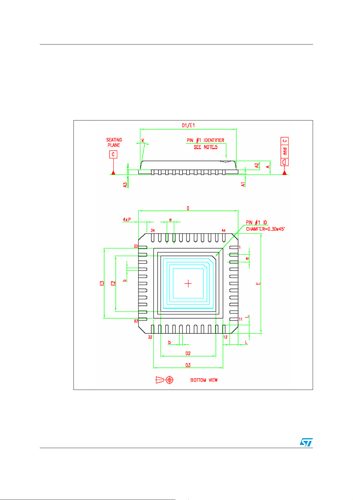
Package mechanical data STW82101B
13 Package mechanical data
In order to meet environmental requirements, ST offers these devices in different grades of
ECOPACK
specifications, grade definitions and product status are available at: www.st.com.
ECOPACK
Figure 31. VFQFPN-44 package outline
®
packages, depending on their level of environmental compliance. ECOPACK®
®
is an ST trademark.
64/68 Doc ID 018503 Rev 3
Page 65
STW82101B Package mechanical data
Table 23. VFQFPN-44 package dimensions
Dimensions in mm
Symbol
Min Typ Max
A 0.80 0.90 1.00
A1 - 0.02 0.05
A2 - 0.65 1.00
A3 - 0.200 -
b 0.18 0.25 0.30
D 6.85 7.00 7.15
D1 - 6.750 -
D2 3.80 3.90 4.00
D3 - 4.90 -
E 6.85 7.00 7.15
E1 - 6.750 -
E2 3.80 3.90 4.00
E3 - 4.90 -
e - 0.50 -
L 0.35 0.55 0.75
P--0.60
K (degree) - - 12
ddd - - 0.08
Note: 1 VFQFPN stands for Thermally Enhanced Very thin Fine pitch Quad Flat Package No lead.
Very thin: A=1.00 Max.
2 Details of terminal 1 identifier are optional but must be located on the top surface of the
package by using either a mold or marked features.
Doc ID 018503 Rev 3 65/68
Page 66
Revision history STW82101B
14 Revision history
Table 24. Document revision history
Date Revision Changes
07-Mar-2011 1 First release
Cover page:
– Noise figure NF changed to 9.5 dB
– Conversion gain CG changed to 8.5 dB
– Removed ‘Preliminary Data’ tags.
Table 3 moved to new Section 3: Absolute maximum ratings
Section 2.1 becomes Section 4: Operating conditions
Section 2.2 becomes Section 5: Test conditions
Section 2.3 becomes Section 6: Electrical characteristics
Table 4: Operating conditions updated current consumption:
. Updated typical values. Added maximum values.
CC3.3V
. Added maximum value for high-current mode at 5.5 V. Updated typical
CC5V
and added maximum value for low-current mode at 3.3 V.
RF-nFLO modified typical values
added maximum value for high-current mode, modified typical value
SSB
and added maximum value for low-current mode
and K
VCOA
split into ΔT
LK
typical values
VCOB
LK A
and ΔT
(for VCOA and VCOB). Specified as
LK B
maximum values.
typical value
DIV4
LOBUF and ILOBUF
lower frequency range typical value
VCOA
typical values
40 MHz
40 MHz
16-Jan-2012 2
–I
–I
Section 6: Electrical characteristics. Added note about Vsupply, RF frequency
range, ambient temperature and RF power conditions.
Table 6: Down converter mixer and IF amplifier electrical characteristics :
updated:
– CG nominal value 8, added minimum and max values.
– IIP3 added minimum values
–nF
–NF
– RF to IF isolation typical value
Table 8: Integer-N synthesizer electrical characteristics updated:
–K
– ΔT
–I
–I4
–K
– modified table footnote 4
Table 9: Phase noise performance updated values of:
– LOA open-loop phase noise @ 1 kHz and 1 MHz, phase noise floor @
– LOB open-loop phase noise @ 1 kHz and 1 MHz, phase noise floor @
Added Section 7: Typical performance characteristics.
Section 8.1.9: Voltage controlled oscillators. Modified sub-sections:
– VCO frequency calibration
– VCO calibration auto-restart feature
66/68 Doc ID 018503 Rev 3
Page 67

STW82101B Revision history
Table 24. Document revision history (continued)
Date Revision Changes
Section 9.3.2: I2C register definitions. Updated description of bitfield CALTYPE
and MUTE_TYPE in registers MUTE_&_CALIBRATION
Added Section 9.4.2: Power ON sequence (I2C interface)
Section 12: Evaluation kit:
– modified Figure 23: SPI timing waveforms
16-Jan-2012 2
11-May-2012 3
– modified Table 19: SPI timing parameters minimum values of t
t
clk_loadf.
clk_loadr
Section 10.3.2: SPI register definitions: updated
– description of bitfields CALTYPE and MUTE_TYPE in register ST2
– description of bitfield PD[4:0] in register ST3
Added Section 10.4.2: Power ON sequence (SPI interface)
Added Section 12: Evaluation kit.
Corrected titles of Figure 7 and Figure 8.
Replaced occurences of ‘STI register’ with ‘SPI register’ in section headers:
– Section 10.3: SPI registers
– Section 10.3.1: SPI register summary
– Section 10.3.2: SPI register definitions.
and
Doc ID 018503 Rev 3 67/68
Page 68

STW82101B
Please Read Carefully:
Information in this document is provided solely in connection with ST products. STMicroelectronics NV and its subsidiaries (“ST”) reserve the
right to make changes, corrections, modifications or improvements, to this document, and the products and services described herein at any
time, without notice.
All ST products are sold pursuant to ST’s terms and conditions of sale.
Purchasers are solely responsible for the choice, selection and use of the ST products and services described herein, and ST assumes no
liability whatsoever relating to the choice, selection or use of the ST products and services described herein.
No license, express or implied, by estoppel or otherwise, to any intellectual property rights is granted under this document. If any part of this
document refers to any third party products or services it shall not be deemed a license grant by ST for the use of such third party products
or services, or any intellectual property contained therein or considered as a warranty covering the use in any manner whatsoever of such
third party products or services or any intellectual property contained therein.
UNLESS OTHERWISE SET FORTH IN ST’S TERMS AND CONDITIONS OF SALE ST DISCLAIMS ANY EXPRESS OR IMPLIED
WARRANTY WITH RESPECT TO THE USE AND/OR SALE OF ST PRODUCTS INCLUDING WITHOUT LIMITATION IMPLIED
WARRANTIES OF MERCHANTABILITY, FITNESS FOR A PARTICULAR PURPOSE (AND THEIR EQUIVALENTS UNDER THE LAWS
OF ANY JURISDICTION), OR INFRINGEMENT OF ANY PATENT, COPYRIGHT OR OTHER INTELLECTUAL PROPERTY RIGHT.
UNLESS EXPRESSLY APPROVED IN WRITING BY TWO AUTHORIZED ST REPRESENTATIVES, ST PRODUCTS ARE NOT
RECOMMENDED, AUTHORIZED OR WARRANTED FOR USE IN MILITARY, AIR CRAFT, SPACE, LIFE SAVING, OR LIFE SUSTAINING
APPLICATIONS, NOR IN PRODUCTS OR SYSTEMS WHERE FAILURE OR MALFUNCTION MAY RESULT IN PERSONAL INJURY,
DEATH, OR SEVERE PROPERTY OR ENVIRONMENTAL DAMAGE. ST PRODUCTS WHICH ARE NOT SPECIFIED AS "AUTOMOTIVE
GRADE" MAY ONLY BE USED IN AUTOMOTIVE APPLICATIONS AT USER’S OWN RISK.
Resale of ST products with provisions different from the statements and/or technical features set forth in this document shall immediately void
any warranty granted by ST for the ST product or service described herein and shall not create or extend in any manner whatsoever, any
liability of ST.
ST and the ST logo are trademarks or registered trademarks of ST in various countries.
Information in this document supersedes and replaces all information previously supplied.
The ST logo is a registered trademark of STMicroelectronics. All other names are the property of their respective owners.
© 2012 STMicroelectronics - All rights reserved
STMicroelectronics group of companies
Australia - Belgium - Brazil - Canada - China - Czech Republic - Finland - France - Germany - Hong Kong - India - Israel - Italy - Japan -
Malaysia - Malta - Morocco - Philippines - Singapore - Spain - Sweden - Switzerland - United Kingdom - United States of America
www.st.com
68/68 Doc ID 018503 Rev 3
 Loading...