

Page 1
查询STF20NM60D供应商
N-CHANNEL 600V - 0.26Ω - 20A TO-220/TO-220FP/TO-247
FDmesh™ POWER MOSFET (with FAST DIODE)
STP20NM60FD - STF20NM60D
STW20NM60FD
TYPE V
STP20NM60FD
STF20NM60D
STW20NM60FD
n TYPICAL R
n HIGH dv/dt AND AVALANCHE CAPABILITIES
n 100% AVALANCHE TESTED
n LOW INPUT CAPACITANCE AND GATE
600 V
600 V
600 V
(on) = 0.26Ω
DS
DSS
R
DS(on)
< 0.29 Ω
< 0.29 Ω
< 0.29 Ω
I
D
20 A
20 A
20 A
Pw
192 W
45 W
214 W
CHARGE
n LOW GATE INPUT RESISTANCE
n TIGHT PROCESS CONTROL AND HIGH
MANUFACTURING YIELDS
DESCRIPTION
The FDmesh™ associates all advan tages of reduced on-resistance and fas t switching with an intrinsic fast-recovery body diode. It is therefore
strongly recommended for bridge topologies, in particular ZVS phase-shift conv ert ers .
APPLICATIONS
n ZVS PHASE-SHIFT FULL BRIDGE
CONVERTERS FOR SMPS A ND WELDING
EQUIPMENT
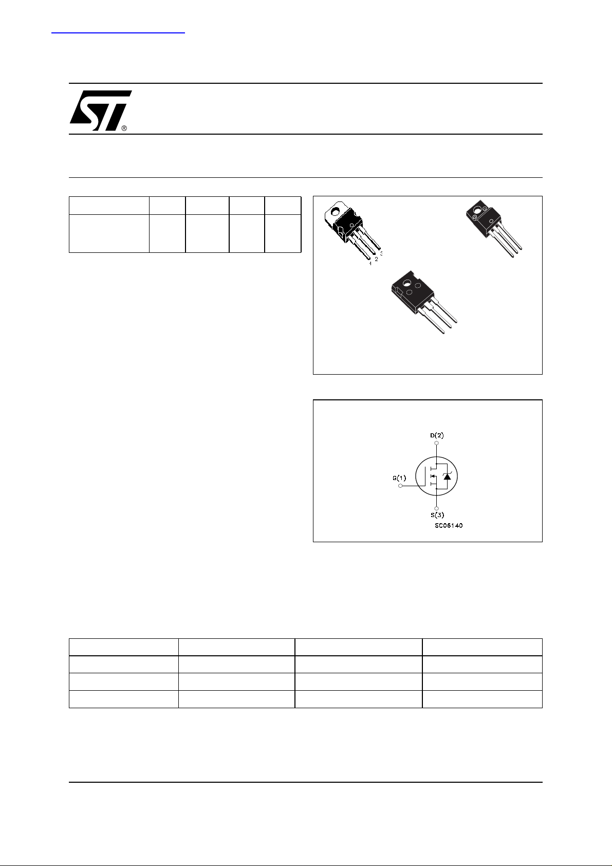
TO-220
1
TO-247
3
2
TO-220FP
INTERNAL SCHEMATIC DIAGRAM
3
2
1
ORDERING INFORMATION
SALES TYPE MARKING PACKAGE PACKAGING
STP20NM60FD P20NM60FD TO-220 TUBE
STF20NM60D F20NM60D TO-220FP TUBE
STW20NM60FD W20NM60FD TO-247 TUBE
1/11June 2003
Page 2
STP20NM60FD - STF20NM 60D - STW20NM60FD
ABSOLUTE MAXIMUM RATINGS
Symbol Parameter Value Unit
STP20NM60FD STF20NM60D STW20NM60FD
V
V
DGR
V
I
I
IDM()
P
TOT
dv/dt (1) Peak Diode Recovery voltage slope 20 V/ns
V
T
T
() Pulse width limited by safe operating area
(1) I
SD
(*) Limited only by maximum temperature allowed
Drain-source Voltage (VGS=0)
DS
Drain-gate Voltage (RGS=20kΩ)
Gate- source Voltage ± 30 V
GS
Drain Current (continuous) at TC= 25°C
D
Drain Current (continuous) at TC= 100°C
D
20 20 (*) 20 A
12.6 12.6 (*) 12.6 A
600 V
600 V
Drain Current (pulsed) 80 80 (*) 80 A
Total Dissipation at TC= 25°C
192 45 214 W
Derating Factor 1.20 0.36 1.42 W/°C
Insulation Withstand Voltage (DC) - 2500 - V
ISO
Operating Junction Temperature
j
Storage Temperature
stg
≤ 20 A, di/dt ≤ 400 A/µs, VDD≤ V
(BR)DSS,Tj≤TJMAX.
–65to150
°C
°C
THERMAL DATA
TO-220 TO-220FP TO-247
Rthj-case Thermal Resistance Junction-case Max 0.65 2.8 0.585 °C/W
Rthj-amb Thermal Resistance Junction-ambient Max 62.5 30 °C/W
T
Maximum Lead Temperature For Soldering Purpose
l
300 °C
AVALANCHE CHARACTERISTICS
Symbol Parameter Max Value Unit
I
AR
E
Avalanche Current, Repetitive or Not-Repetitive
(pulse width limited by T
Single Pulse Avalanche Energy
AS
(starting T
=25°C,ID=IAR,VDD=35V)
j
max)
j
10 A
700 mJ
2/11
Page 3
STP20NM60FD - ST F20NM60D - STW20NM60FD
ELECTRICAL CHARACTERISTICS (T
=25°C UNLESS OTHERWISE SP ECIFIED)
CASE
ON/OFF
Symbol Parameter Test Conditions Min. Typ. Max. Unit
V
(BR)DSS
Drain-source
ID= 250 µA, VGS= 0 600 V
Breakdown Voltage
I
DSS
I
GSS
V
GS(th)
R
DS(on)
Zero Gate Voltage
Drain Current (V
GS
=0)
Gate-body Leakage
Current (V
DS
=0)
Gate Threshold Voltage
Static Drain-source On
V
= Max Rating
DS
VDS= Max Rating, TC= 125 °C
V
= ±30V ±100 µA
GS
V
DS=VGS,ID
= 250µA
345V
1
10
VGS=10V,ID= 10 A 0.26 0.29 Ω
Resistance
DYNAMIC
Symbol Parameter Test Conditions Min. Typ. Max. Unit
(1) Forward Transconductance VDS>I
g
fs
D(on)xRDS(on)max,
9S
ID= 10A
C
iss
C
oss
C
rss
C
oss eq.
Input Capacitance
Output Capacitance
Reverse Transfer
Capacitance
(3) Equivalent Output
=25V,f=1MHz,VGS= 0 1310
V
DS
580
30
VGS=0V,VDS= 0V to 480V 190 pF
Capacitance
R
G
Gate Input Resistance f=1 MHz Gate DC Bias = 0
2.7 Ω
Test Signal Level = 20mV
Open Drain
SWITCHING ON
Symbol Parameter Test Conditions Min. Typ. Max. Unit
t
d(on)
Q
Q
Q
Turn-on Delay Time
t
r
g
gs
gd
Rise Time
Total Gate Charge
Gate-Source Charge
Gate-Drain Charge
VDD=300V,ID= 10A
RG= 4.7Ω VGS=10V
(Resistive Load see, Figure 3)
=480V,ID= 20A,
V
DD
V
=10V
GS
25
12
37
10
17
52
µA
µA
pF
pF
pF
ns
ns
nC
nC
nC
SWITCHING OFF
Symbol Parameter Test Conditions Min. Typ. Max. Unit
= 480 V, ID= 20A,
t
r(Voff)
t
t
Off-voltage Rise Time
f
c
Fall Time
Cross-over Time
V
DD
=4.7Ω, VGS= 10V
R
G
(Inductive Load see, Figure 5)
8
22
30
SOURCE DRAIN DIODE
Symbol Parameter Test Conditions Min. Typ. Max. Unit
I
SD
I
SDM
V
SD
t
rr
Q
rr
I
RRM
Note: 1. Pulsed: Pulse duration = 300 µs, duty cycle 1.5 %.
2. Pulse width limited by safe o perating area.
3. C
Source-drain Current
(2)
Source-drain Current (pulsed)
(1)
Forward On Voltage
Reverse Recovery Time
Reverse Recovery Charge
Reverse Recovery Current
is defined as a constant equivalent capacitance giving the same charging time as C
oss eq.
ISD=20A,VGS=0
I
SD
V
DD
(see test circuit, Figure 5)
= 20 A, di/dt = 100A/µs,
=60V,Tj= 150°C
340
2.8
17
when VDSincreases from 0 to 80%
oss
20
80
1.5 V
ns
ns
ns
A
A
ns
µC
A
3/11
Page 4
STP20NM60FD - STF20NM 60D - STW20NM60FD
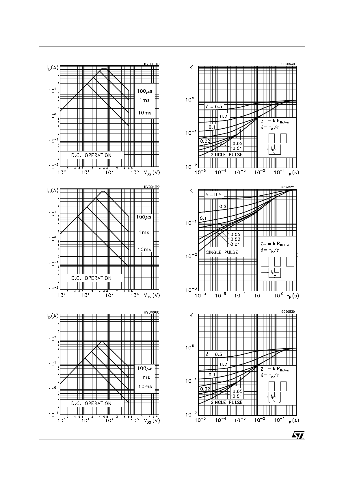
Thermal Impedance For TO-220Safe Operating Area For TO-220
Safe Operating Area For TO-220FP Thermal Imped ance For TO-220FP
4/11
Thermal Impedance For TO-247Safe Operating Area For TO-247
Page 5

STP20NM60FD - ST F20NM60D - STW20NM60FD
Output Characteristics
Transfer Characteristics
Static Drain-source O n ResistanceTransconductance
Gate Charge vs Gate-so urce Voltage
Capacitance Variations
5/11
Page 6

STP20NM60FD - STF20NM 60D - STW20NM60FD
Normalized On Resistance vs TemperatureNormalized Gate Threshold Voltage vs Temp.
Source-drain Diode Forward Characteristics
6/11
Page 7

STP20NM60FD - ST F20NM60D - STW20NM60FD
Fig. 2: Unclamped Inductive WaveformFig. 1: Unclamped Inductive Load Test Circuit
Fig. 3: Switching Times Test Circuit For
Resistive Load
Fig. 5: Test Circuit For Induc t ive Load Switching
And Diode Recovery Times
Fig. 4: Gate Charge test Circuit
7/11
Page 8

STP20NM60FD - STF20NM 60D - STW20NM60FD
TO-220 MECHANICAL DATA
DIM.
A 4.40 4.60 0.173 0.181
b 0.61 0.88 0.024 0.034
b1 1.15 1.70 0.045 0.066
c 0.49 0.70 0.019 0.027
D 15.25 15.75 0.60 0.620
E 10 10.40 0.393 0.409
e 2.40 2.70 0.094 0.106
e1 4.95 5.15 0.194 0.202
F 1.23 1.32 0.048 0.052
H1 6.20 6.60 0.244 0.256
J1 2.40 2.72 0.094 0.107
L 13 14 0.511 0.551
L1 3.50 3.93 0.137 0.154
L20 16.40 0.645
L30 28.90 1.137
øP 3.75 3.85 0.147 0.151
Q 2.65 2.95 0.104 0.116
MIN. TYP MAX. MIN. TYP. MAX.
mm. inch
8/11
Page 9

STP20NM60FD - ST F20NM60D - STW20NM60FD
TO-220FP MECHANICAL DATA
DIM.
A 4.4 4.6 0.173 0.181
B 2.5 2.7 0.098 0.106
D 2.5 2.75 0.098 0.108
E 0.45 0.7 0.017 0.027
F 0.75 1 0.030 0.039
F1 1.15 1.7 0.045 0.067
F2 1.15 1.7 0.045 0.067
G 4.95 5.2 0.195 0.204
G1 2.4 2.7 0.094 0.106
H 10 10.4 0.393 0.409
L2 16 0.630
L3 28.6 30.6 1.126 1.204
L4 9.8 10.6 .0385 0.417
L5 2.9 3.6 0.114 0.141
L6 15.9 16.4 0.626 0.645
L7 9 9.3 0.354 0.366
Ø 3 3.2 0.118 0.126
MIN. TYP MAX. MIN. TYP. MAX.
mm. inch
E
A
D
B
L3
L6
L7
F1
F
G1
H
F2
123
L4
L2
L5
G
9/11
Page 10

STP20NM60FD - STF20NM 60D - STW20NM60FD
TO-247 MECHANICAL DATA
DIM.
A 4.85 5.15 0.19 0.20
A1 2.20 2.60 0.086 0.102
b 1.0 1.40 0.039 0.055
b1 2.0 2.40 0.079 0.094
b2 3.0 3.40 0.118 0.134
c 0.40 0.80 0.015 0.03
D 19.85 20.15 0.781 0.793
E 15.45 15.75 0.608 0.620
e5.45 0.214
L 14.20 14.80 0.560 0.582
L1 3.70 4.30 0.14 0.17
L2 18.50 0.728
øP 3.55 3.65 0.140 0.143
øR 4.50 5.50 0.177 0.216
S5.50 0.216
MIN. TYP MAX. MIN. TYP. MAX.
mm. inch
10/11
Page 11

STP20NM60FD - ST F20NM60D - STW20NM60FD
Information furnished is believed to be accurate and reliable. However, STMicroelectronics assumes no responsibility for the
consequences of u se of such inf ormat ion nor for any in fring ement of p aten ts or othe r ri ghts of th ird p arties whic h may resul t f rom
its use. No license is granted by implication or otherwise under any patent or patent rights of STMicroelectronics. Specifications
mentioned in this publication are subject to change without notice. This publication supersedes and replaces all information
previously supplied. STMicroelectronics products are not authorized for use as critical components in life support devices or
systems without express written approval of STMicroelectronics.
Australia - Brazil - Canada - China - Finland - France - Germany - Hong Kong - India - Israel - Italy - Japan - Malaysia - Malta - Morocco
© The ST logo is a registered trademark of STMicroelectronics
© 2003 STMicroelectronics - Printed in Italy - All Rights Reserved
Singapore - Spain - Sweden - Switzerland - United Kingdom - United States.
STMicroelectronics GROUP OF COMPANIES
© http://www.st.com
11/11
 Loading...