

Page 1
STW20NM50FD
N-CHANNEL 500V - 0.22Ω - 20A TO-247
FDmesh™ Power MOSFET (with FAST DIODE)
TYPE V
DSS
R
DS(on)
I
D
STW20NM50 FD 500V <0.25Ω 20 A
■ TYPICAL R
■ HIGH dv/dt AND AVALANCHE CAPABILITIES
■ 100% AVALANCHE TESTED
■ LOW INPUT CAPACITANCE AND GATE CHARGE
■ LOW GATE INPUT RESIST AN C E
■ TIGHT PROCESS CONTROL AND HIGH
(on) = 0.22Ω
DS
MANUFACTURING YIELDS
DESCRIPTION
The FDmesh™
associates all advantage s of red uced
on-resistance and fast switching with an intrinsic fastrecovery body diode. It is therefore strongly recommended for bridge topologies, in particular ZVS phaseshift conve r te rs.
APPLICATIONS
■ ZVS PHASE-SH IFT FULL BRIDGE CONVERTERS
FOR SMPS AND WELDIN G EQUI PMEN T
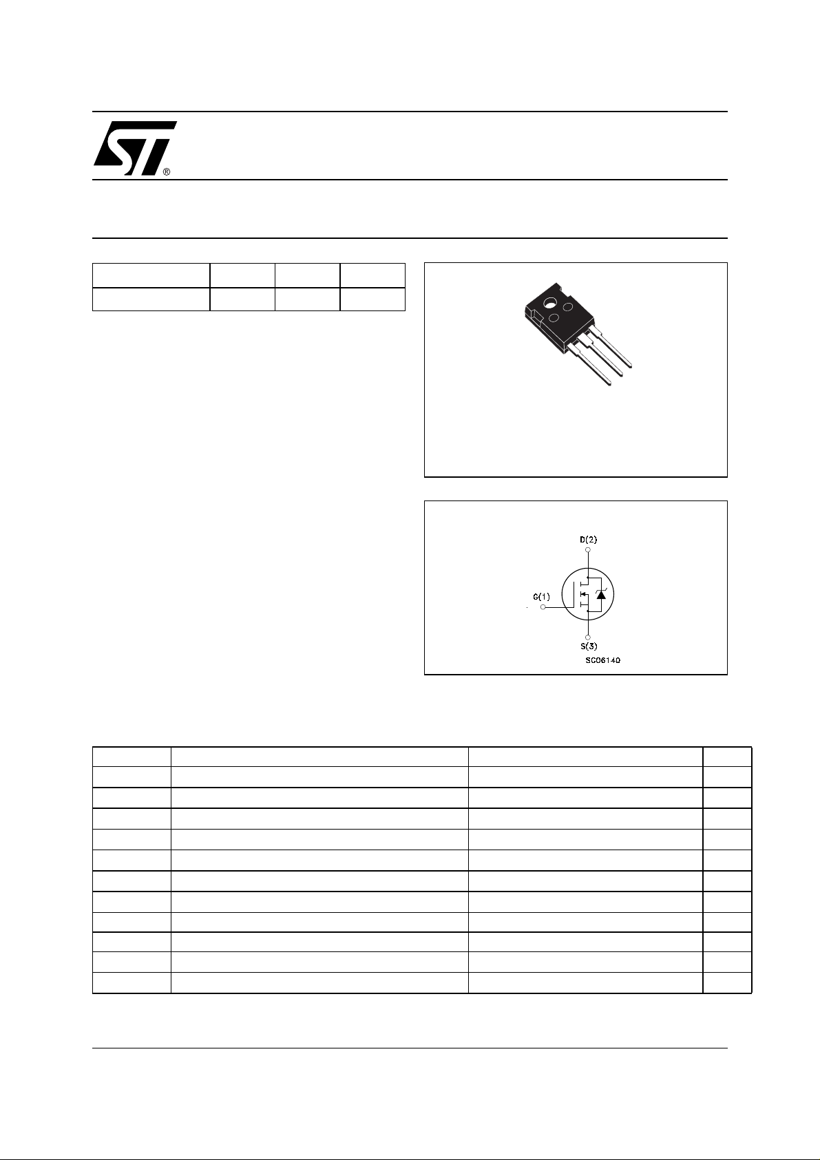
3
2
1
TO-247
I
NTERNAL SCHEMATIC DIAGRAM
ABSOLUTE MAXIMUM RATINGS
Symbol Parameter Value Unit
V
DS
V
DGR
V
GS
I
D
I
D
IDM (●)
P
TOT
dv/dt(1) Peak Diode Recovery voltage slope 20 V/ns
T
stg
T
j
(•)Pu l se width limite d by safe operating area
Drain-source Voltage (VGS = 0)
Drain-gate Voltage (RGS = 20 kΩ)
500 V
500 V
Gate- source Voltage ±30 V
Drain Current (continuos) at TC = 25°C
Drain Current (continuos) at TC = 100°C
20 A
14 A
Drain Current (pulsed) 80 A
Total Dissipation at TC = 25°C
214 W
Derating Factor 1.42 W/°C
Storage Temperature –65 to 150 °C
Max. Operating Junction Temperature 150 °C
(1)ISD ≤20A, di/dt ≤400A/µs, VDD ≤ V
(*)Limit ed only by maximum temperat ure allowed
(BR)DSS
, Tj ≤ T
JMAX.
1/8June 2002
Page 2
STW20NM50FD
THERMA L D ATA
Rthj-case Thermal Resistance Junction-case Max 0.585 °C/W
Rthj-amb Thermal Resistance Junction-ambient Max 30 °C/W
T
l
AVALANCHE CHARACTERISTICS
Symbol Parameter Max Value Unit
I
AR
E
AS
ELECTRICAL CHARACTERISTICS (TCASE = 25 °C UNLESS OTHERWISE SPECIFIED)
OFF
Symbol Parameter Test Conditions Min. Typ. Max. Unit
V
(BR)DSS
I
DSS
I
GSS
Maximum Lead Temperature For Soldering Purpose 300 °C
Avalanche Current, Repetitive or Not-Repetitive
(pulse width limited by T
max)
j
Single Pulse Avalanche Energy
(starting T
Drain-source
= 25 °C, ID = IAR, VDD = 35 V)
j
ID = 250 µA, VGS = 0 500 V
10 A
700 mJ
Breakdown Voltage
Zero Gate Voltage
Drain Current (V
GS
Gate-body Leakage
Current (V
DS
= 0)
= 0)
V
= Max Rating
DS
V
= Max Rating, TC = 125 °C
DS
V
= ±30V ±100 nA
GS
1µA
10 µA
ON
(1)
Symbol Parameter Test Conditions Min. Typ. Max. Unit
V
GS(th)
R
DS(on)
Gate Threshold Voltage
Static Drain-source On
V
= VGS, ID = 250µA
DS
345V
VGS = 10V, ID = 10A 0.22 0.25 Ω
Resistance
DYNAMIC
Symbol Parameter Test Conditions Min. Typ. Max. Unit
gfs (1) Forward Transconductance VDS > I
ID= 10A
C
iss
C
oss
C
rss
Input Capacitance
Output Capacitance 290 pF
Reverse Transfer
Capacitance
C
oss eq.
(2) Equivalent Output
VGS = 0V, VDS = 0V to 400V 130 pF
Capacitance
R
g
Gate Input Resistance f=1 MHz Gate DC Bias=0
Test Signal Level=20mV
Open Drain
1. Pulsed: Pu l se duration = 300 µs, duty cyc l e 1.5 %.
2. C
is defined as a constant equivalent capacitance giving the same charging time as C
oss eq.
V
.
DSS
V
DS
D(on)
x R
DS(on)max,
= 25V, f = 1 MHz, VGS = 0
9S
1380 pF
40 pF
2.8 Ω
when VDS increase s fr om 0 to 80%
oss
2/8
Page 3
STW20NM50FD
ELECTRICAL CHARACTERISTICS (CONTINUED)
SWITCHING ON
Symbol Parameter Test Conditions Min. Typ. Max. Unit
V
t
d(on)
Q
Q
Q
t
r
g
gs
gd
Turn-on Delay Time
Rise Time 20 ns
Total Gate Charge
Gate-Source Charge 18 nC
Gate-Drain Charge 10 nC
SWITCHING OFF
Symbol Parameter Test Conditions Min. Typ. Max. Unit
t
r(Voff)
t
f
t
c
Off-voltage Rise Time
Fall Time 15 ns
Cross-over Time 30 ns
SOURCE DRAIN DIODE
Symbol Parameter Test Conditions Min. Typ. Max. Unit
I
SD
I
SDM
VSD (1)
t
rr
Q
rr
I
RRM
Note: 1. Pulsed: Pu l se duration = 300 µs, duty cycle 1.5 %.
2. Pulse width l i m i ted by safe oper ating area.
Source-drain Current 20 A
(2)
Source-drain Current (pulsed) 80 A
Forward On Voltage
Reverse Recovery Time
Reverse Recovery Charge 2 µC
Reverse Recovery Current 16 A
= 250V, ID = 10 A
DD
RG= 4.7Ω VGS = 10V
(see test circuit, Figure 3)
V
= 400V, ID = 20A,
DD
VGS = 10V
V
= 400V, ID = 20 A,
DD
RG=4.7Ω, V
GS
= 10V
(see test circuit, Figure 5)
ISD = 20 A, VGS = 0
I
= 20 A, di/dt = 100A/µs,
SD
VDD = 60V, Tj = 150°C
(see test circuit, Figure 5)
22 ns
38 53 nC
6ns
1.5 V
245 ns
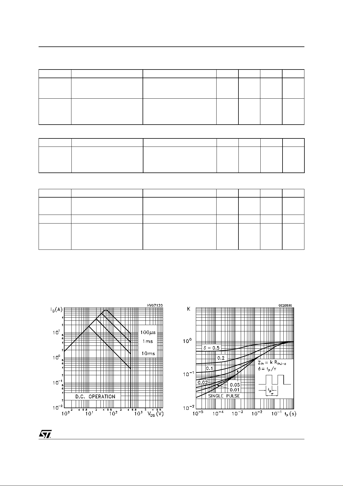
Safe Operating Area Thermal Impedance
3/8
Page 4

STW20NM50FD
Output Characteristics
Transconductance
Transfer Characteristics
Static Drain-source On Resistance
Gate Charge vs Gate-source Voltage
4/8
Capacitance Variations
Page 5

Source-drain Diode Forward Characteristics
STW20NM50FD
Normalized On Resistance vs Temperatur eNormalized Gate Thereshold Voltage vs Temp.
5/8
Page 6

STW20NM50FD
Fig. 2: Unclamped Inductive WaveformFig. 1: Unclamped Inductive Load Test Circuit
Fig. 3: Switching Times Test Circuits For
Resistive Load
Fig. 5: Test Circuit For Inductive Load Switching
And Diode Recovery Times
Fig. 4: Gate Charge test Circuit
6/8
Page 7

TO-247 MECHANICAL DATA
STW20NM50FD
DIM.
A 4.85 5.15 0.19 0.20
D 2.20 2.60 0.08 0.10
E 0.40 0.80 0.015 0.03
F 1 1.40 0.04 0.05
F1 3 0.11
F2 2 0.07
F3 2 2.40 0.07 0.09
F4 3 3.40 0.11 0.13
G 10.90 0.43
H 15.45 15.75 0.60 0.62
L 19.85 20.15 0.78 0.79
L1 3.70 4.30 0.14 0.17
L2 18.50 0.72
L3 14.20 14.80 0.56 0.58
L4 34.60 1.36
L5 5.50 0.21
M 2 3 0.07 0.11
V
V2
Dia 3.55 3.65 0.14 0.143
MIN. TYP MAX. MIN. TYP. MAX.
mm. inch
5º5º
60º 60º
7/8
Page 8

STW20NM50FD
8/8
Information furnished is believed to be accurate and reliable. However, STMicroelectronics assumes no responsibility for the consequences
of use of such inform ation nor for a ny in fringem ent of patents or o ther rig hts of third part ies which may result from its u se. N o l i cen se i s
granted by implication or otherwise under any patent or patent rights of STMicroelectronics. Specification mentioned in this publication are
subject to change without notice. This publication supersedes and replaces all information previously supplied. STMicroelectronics products
are not authorized for use as critical compo nents in life support devices or systems without express written approval of STMicroelectronics.
Australia - Brazil - China - Finland - France - Germany - Hong Kong - India - Italy - Japan - Malaysia - Malta - Morocco -
The ST logo is a trademark of STMicroelectronics
© 2000 STMicroelectronics – Printed in Italy – All Rights Reserved
STMicroelectronics GROUP OF COMPANIES
Singapore - Spain - Sweden - Switzerland - United Kingdom - U.S.A.
http://www.st.com
 Loading...