

Page 1
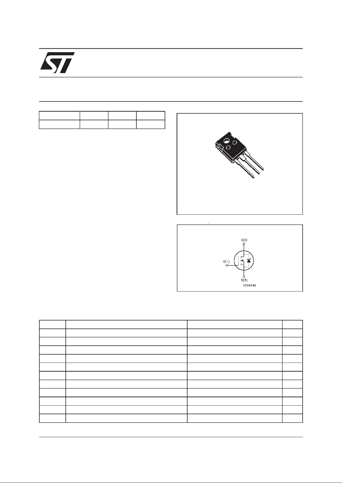
STW20NB50
N - CHANNEL 500V - 0.22Ω - 20A - TO-247
PowerMESH MOSFET
TYPE V
DSS
R
DS(on)
I
D
ST W20NB 50 500 V < 0.25 Ω 20 A
■ TYPICALR
■ EXTREMELYHIGH dv/dt CAPABILITY
■ ± 30V GATE TO SOURCEVOLTAGERATING
■ 100%AVALANCHETESTED
■ REPETITIVEAVALANCHEDATA AT 100
■ VERYLOW INTRINSIC CAPACITANCES
■ GATECHARGE MINIMIZED
DS(on)
= 0.22 Ω
o
C
DESCRIPTION
Using the latest high voltage technology,
STMicroelectronics has designed an advanced
family of power Mosfets with outstanding
performances. The new patent pending strip
layout coupled with the Company’s proprietary
edge termination structure, gives the lowest
R
(on) per area, exceptional avalanche and
DS
dv/dt capabilities and unrivalled gate charge and
switchingcharacteristics.
APPLICATIONS
■ HIGHCURRENT, HIGHSPEEDSWITCHING
■ SWITCHMODE POWER SUPPLIES(SMPS)
■ DC-AC CONVERTERS FOR WELDING
EQUIPMENTAND UNINTERRUPTIBLE
POWERSUPPLIESAND MOTORDRIVE
3
2
1
TO-247
INTERNAL SCHEMATIC DIAGRAM
ABSOLUTE MAXIMUM RATINGS
Symbol Parameter Value Unit
V
V
V
I
DM
P
dv/dt(
T
(•) Pulse width limited by safe operating area (1)ISD≤ 20A, di/dt ≤ 200 A/µs, VDD≤ V
October 1999
Drain-source Volta ge (VGS=0) 500 V
DS
Drain- gate Voltage (RGS=20kΩ)
DGR
Gat e-source V oltage ± 30 V
GS
I
Drain Curre nt (cont in uous) at Tc=25oC20A
D
I
Drain Curre nt (cont in uous) at Tc= 100oC 12.7 A
D
500 V
(•) Drain Current (pu lsed) 80 A
Tot al Dissipat ion a t Tc=25oC250W
tot
Derating F act or 2 W/
1) Peak Diode Recover y volt age slope 4 V/ns
Sto rage Tem peratu r e -65 to 15 0
stg
T
Max. Operati ng J unction Temperatu r e 150
j
,Tj≤T
(BR)DSS
JMAX
o
C
o
C
o
C
1/8
Page 2
STW20NB50
THERMAL DATA
R
thj-case
R
thj-amb
R
thc-sink
T
AVALANCHE CHARACTERISTICS
Symbol Para meter Max V alue Uni t
I
AR
E
Ther mal Res is t an c e Junc ti on-case Max
Ther mal Res is t an c e Junc ti on-amb ient Max
Thermal Resistance Case-sink Typ
Maximum Le ad Temper at u r e Fo r Sold ering P ur p os e
l
Avalanche Cu r rent, Repetit ive or Not-Re petit iv e
(pulse width limited by T
Single Pulse Ava lanche Energy
AS
(starting T
=25oC, ID=IAR,VDD=50V)
j
max, δ <1%)
j
0.5
30
0.1
300
20 A
1000 mJ
o
C/W
oC/W
o
C/W
o
C
ELECTRICAL CHARACTERISTICS
=25oC unless otherwisespecified)
(T
case
OFF
Symbol Parameter Test Condit ions Min. Typ. Max. Unit
V
(BR)DSS
Drain-sou rc e
=250µAVGS=0
I
D
500 V
Break d own Voltage
I
DSS
I
GSS
Zero Gate Voltage
Drain Current (V
GS
Gat e- b ody Le akage
Current (V
DS
=0)
=0)
V
=MaxRating
DS
= Max Rating Tc=125oC
V
DS
= ± 30 V
V
GS
10
100
± 100 nA
ON(∗)
Symbol Parameter Test Condit ions Min. Typ. Max. Unit
V
GS(th)
Gate Threshold
V
DS=VGSID
= 250 µA
345V
Voltage
R
DS(on)
Static Drain-source O n
VGS=10V ID= 10 A 0.22 0.2 5
Resistance
I
D(on)
On State Dra in Cur rent VDS>I
D(on)xRDS(on)max
20 A
VGS=10V
DYNAMIC
Symbol Parameter Test Condit ions Min. Typ. Max. Unit
g
(∗)Forward
fs
Tr anscond uctance
C
C
C
Input Capaci t an c e
iss
Out put Capacitance
oss
Reverse Transf er
rss
Capacitance
VDS>I
D(on)xRDS(on)maxID
=10A 9 13.5 S
VDS=25V f=1MHz VGS= 0 3600
460
55
4700
600
75
µA
µA
Ω
pF
pF
pF
2/8
Page 3
STW20NB50
ELECTRICAL CHARACTERISTICS
(continued)
SWITCHINGON
Symbol Parameter Test Condit ions Min. Typ. Max. Unit
t
d(on)
t
r
Turn-on Time
Rise Time
VDD= 250 V ID=10A
R
=4.7
G
Ω
VGS=10V
32
15
43
21
(see test circuit, figure 3)
Q
Q
Q
Total Gate Charge
g
Gat e- Sour ce Cha rge
gs
Gate-Drain Charge
gd
VDD= 400 V ID=20A VGS=10V 85
21
37
110 nC
SWITCHINGOFF
Symbol Parameter Test Condit ions Min. Typ. Max. Unit
t
r(Voff)
t
t
Off -voltage Rise Time
Fall Time
f
Cross-over Ti m e
c
VDD= 400 V ID=20A
=4.7 ΩVGS=10V
R
G
(see test circuit, figure 5)
20
25
47
27
33
62
SOURCEDRAINDIODE
Symbol Parameter Test Condit ions Min. Typ. Max. Unit
I
SD
I
SDM
V
SD
t
Q
I
RRM
(∗) Pulsed: Pulse duration = 300 µs, duty cycle 1.5 %
(•) Pulse width limited by safe operatingarea
Source-drain Curr ent
(•)
Source-drain Curr ent
20
80
(pulsed)
(∗) For ward On V oltage ISD=20A VGS=0 1.6 V
Reverse Recovery
rr
Time
Reverse Recovery
rr
= 20 A di / dt = 100 A/µs
I
SD
= 100 V Tj=150oC
V
DD
(see test circuit, figure 5)
700
9
Charge
Reverse Recovery
25
Current
ns
ns
nC
nC
ns
ns
ns
A
A
ns
µ
A
C
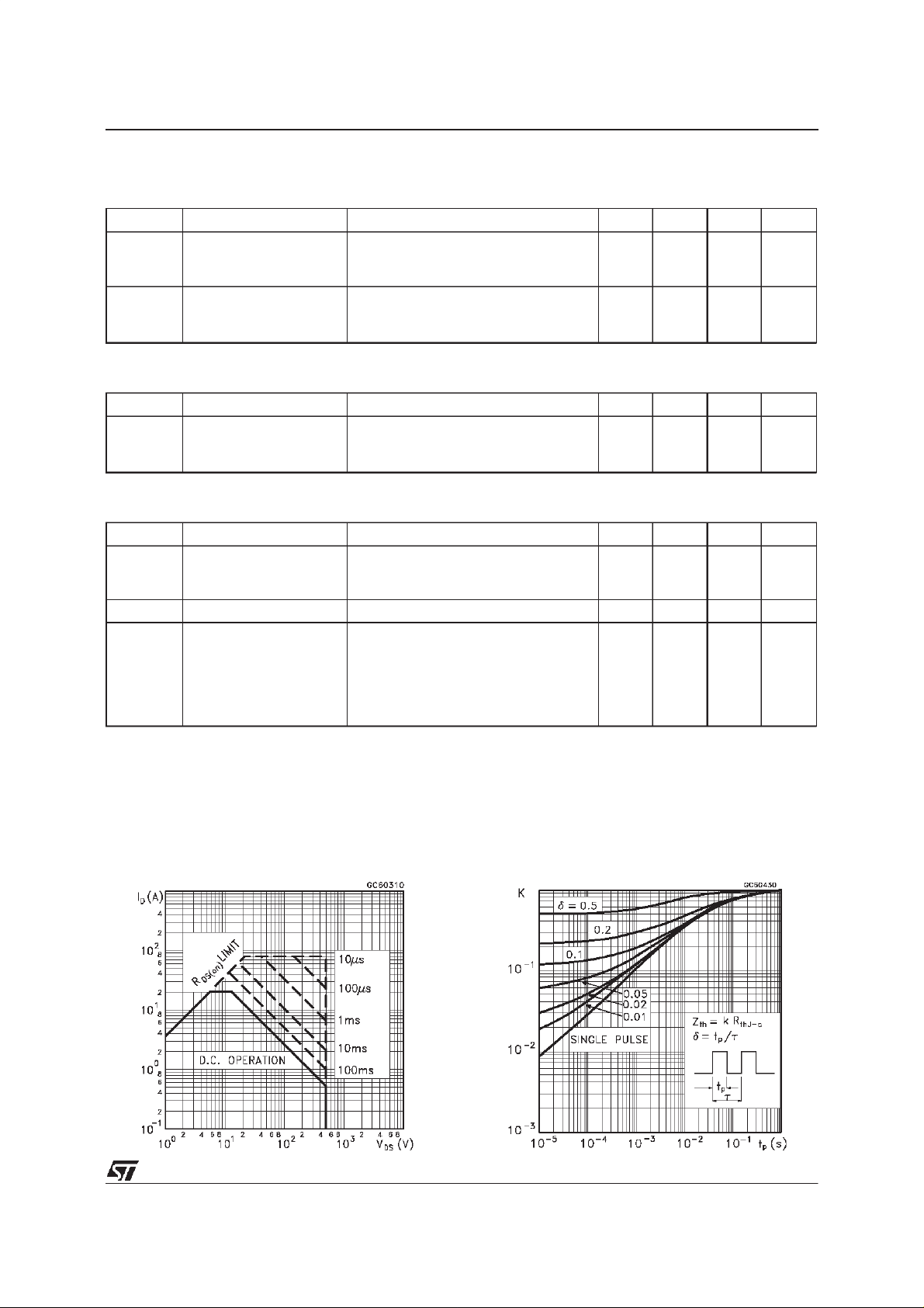
SafeOperating Area ThermalImpedance
3/8
Page 4

STW20NB50
OutputCharacteristics
Transconductance
TransferCharacteristics
Static Drain-sourceOn Resistance
Gate Charge vs Gate-sourceVoltage
4/8
CapacitanceVariations
Page 5

STW20NB50
Normalized Gate ThresholdVoltage vs
Temperature
Source-drainDiode Forward Characteristics
Normalized On Resistance vsTemperature
5/8
Page 6

STW20NB50
Fig. 1:
UnclampedInductiveLoad TestCircuit
Fig. 3: SwitchingTimes Test Circuits For
ResistiveLoad
Fig. 2:
UnclampedInductive Waveform
Fig. 4: GateChargetest Circuit
Fig. 5:
Test CircuitFor InductiveLoad Switching
And Diode Recovery Times
6/8
Page 7

TO-247 MECHANICAL DATA
STW20NB50
DIM.
MIN. TYP. MAX. MIN. TYP. MAX.
A 4.7 5.3 0.185 0.209
D 2.2 2.6 0.087 0.102
E 0.4 0.8 0.016 0.031
F 1 1.4 0.039 0.055
F3 2 2.4 0.079 0.094
F4 3 3.4 0.118 0.134
G 10.9 0.429
H 15.3 15.9 0.602 0.626
L 19.7 20.3 0.776 0.779
L3 14.2 14.8 0.559 0.582
L4 34.6 1.362
L5 5.5 0.217
M 2 3 0.079 0.118
mm inch
P025P
7/8
Page 8

STW20NB50
Information furnished is believed to be accurate and reliable.However, STMicroelectronics assumes no responsibility for the consequences
of use of such information nor for any infringement of patents or other rights of third parties which may result from its use. No license is
granted by implication or otherwise under any patent or patent rights of STMicroelectronics. Specification mentioned in this publication are
subjecttochange without notice. This publication supersedes and replaces all information previouslysupplied. STMicroelectronicsproducts
are not authorized for use as critical components in life support devices or systemswithout express written approval of STMicroelectronics.
The ST logo is a trademark of STMicroelectronics
1999 STMicroelectronics – Printed in Italy – All Rights Reserved
STMicroelectronics GROUP OF COMPANIES
Australia - Brazil - China - Finland - France - Germany - Hong Kong - India - Italy - Japan- Malaysia - Malta - Morocco -
8/8
Singapore - Spain - Sweden - Switzerland - United Kingdom - U.S.A.
http://www.st.com
.
 Loading...