

Page 1
STW16NB60
N-CHANNEL 600V - 0.3Ω -16ATO-247
PowerMesh™ MOSFET
TYPE V
DSS
R
DS(on)
I
D
STW16NB60 600V < 0.35 Ω 16 A
■ TYPICAL R
■ EXTREMELY HIGHdv/dt CAPABILITY
■ 100% AVALANCHE TESTED
■ VERY LOW INTRINSICCAPACITANCES
■ GATE CHARGE MINIMIZED
(on) = 0.3Ω
DS
DESCRIPTION
Using the latest high voltage MESH OVERLAY™
process, STMicroelectronics has des igned an a dvanced family of power MOS FETs with outstanding
performances. The n ew patent pending strip l ay out
coupled with the Company’s proprieratyedge termination structure, gives the lowest RDS (on) per area,
exceptional avalanche and dv/dt capabilities and
unrivalled gate charge and switching characteristics.
APPLICATIONS
■ SWITCH MODE POWER SUPPLIES (SMPS)
■ DC-AC CONVERTERS FOR WELDING
EQUIPMENT AND UNINTERRUPTIBLE
POWER SUPPLIES AND MOTOR DRIVE
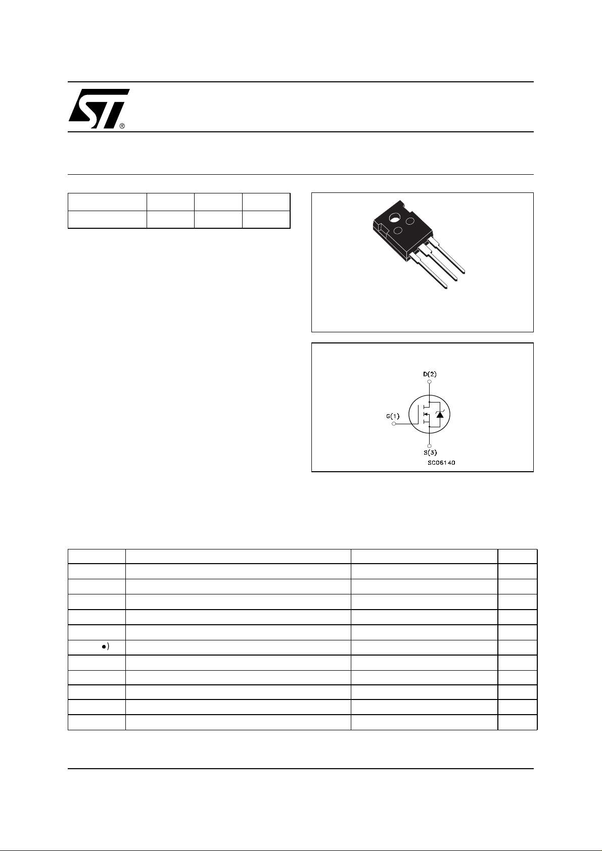
3
2
1
TO-247
INTERNAL SCHEMATIC DIAGRAM
ABSOLUTE MAXIMUM RATINGS
Symbol Parameter Value Unit
V
DS
V
DGR
V
GS
I
D
I
D
I
DM
P
TOT
dv/dt(1) Peak Diode Recovery voltage slope 4 V/ns
T
stg
T
(•)Pulse width limited by safe operating area
Drain-source Voltage (VGS=0)
Drain-gate Voltage (RGS=20kΩ)
600 V
600 V
Gate- source Voltage ±30 V
Drain Current (continuos) at TC= 25°C
Drain Current (continuos) at TC= 100°C
()
Drain Current (pulsed) 64 A
Total Dissipation at TC= 25°C
16 A
10 A
220 W
Derating Factor 1.76 W/°C
Storage Temperature –65 to 150 °C
Max. Operating Junction Temperature 150 °C
j
(1)ISD≤16A, di/dt ≤100A/µs, VDD≤ V
(BR)DSS,Tj≤TJMAX.
1/8April 2003
Page 2
STW16NB60
THERMAL DATA
Rthj-case Thermal Resistance Junction-case Max 0.567 °C/W
Rthj-amb Thermal Resistance Junction-ambient Max 30 °C/W
T
AVALANCHE CHARACTERISTICS
Symbol Parameter Max Value Unit
I
AR
E
AS
ELECTRICAL CHARACTERISTICS (TCASE = 25 °C UNLESS OTHERWISE SPECIFIED)
OFF
Symbol Parameter Test Conditions Min. Typ. Max. Unit
V
(BR)DSS
I
DSS
I
GSS
Maximum Lead Temperature For Soldering Purpose 300 °C
l
Avalanche Current, Repetitive or Not-Repetitive
(pulse width limited by T
max)
j
Single Pulse Avalanche Energy
(starting T
Drain-source
= 25 °C, ID=IAR,VDD=50V)
j
ID= 250 µA, VGS= 0 600 V
16 A
600 mJ
Breakdown Voltage
= Max Rating
V
Zero Gate Voltage
Drain Current (V
GS
Gate-body Leakage
Current (V
DS
=0)
=0)
DS
= Max Rating, TC= 125 °C
V
DS
V
= ±30V ±100 nA
GS
1µA
50 µA
ON (1)
Symbol Parameter Test Conditions Min. Typ. Max. Unit
V
GS(th)
R
DS(on)
Gate Threshold Voltage
Static Drain-source On
V
DS=VGS,ID
VGS=10V,ID=8A
= 250 µA
345V
0.3 0.35 Ω
Resistance
DYNAMIC
Symbol Parameter Test Conditions Min. Typ. Max. Unit
g
fs
Forward Transconductance VDS>I
D(on)xRDS(on)max,
ID=8A
C
iss
C
oss
C
rss
Input Capacitance
Output Capacitance 465 pF
Reverse Transfer
V
=25V,f=1MHz,VGS=0
DS
Capacitance
14.5 S
3300 pF
45 pF
2/8
Page 3
STW16NB60
ELECTRICAL CHARACTERISTICS (CONTINUED)
SWITCHING ON
Symbol Parameter Test Conditions Min. Typ. Max. Unit
t
d(on)
Q
Q
Q
t
r
gs
gd
Turn-on Delay Time
Rise Time
Total Gate Charge
g
Gate-Source Charge 19.5 nC
Gate-Drain Charge 35 nC
SWITCHING OFF
Symbol Parameter Test Conditions Min. Typ. Max. Unit
t
r(Voff)
t
t
f
c
Off-voltage Rise Time
Fall Time 12 ns
Cross-over Time 30 ns
SOURCE DRAIN DIODE
Symbol Parameter Test Conditions Min. Typ. Max. Unit
I
SD
I
SDM
VSD(1)
t
rr
Q
rr
I
RRM
Note: 1. Pulsed: Pulse duration = 300 µs, duty cycle 1.5 %.
2. Pulse width limited by safe o perating area.
Source-drain Current 16 A
(2)
Source-drain Current (pulsed) 64 A
Forward On Voltage
Reverse Recovery Time
Reverse Recovery Charge 11 µC
Reverse Recovery Current 27 A
VDD= 300V, ID=8A
R
= 4.7Ω,VGS= 10V
G
(see test circuit, Figure 3)
V
= 480V, ID=16A,
DD
=10V,RG=4.7Ω
V
GS
V
=480V,ID=16A,
DD
RG= 4.7Ω, VGS=10V
(see test circuit, Figure 5)
ISD=16A,VGS=0
I
= 16 A, di/dt = 100 A/µs,
SD
= 100V, Tj= 150°C
V
DD
(see test circuit, Figure 5)
35 ns
16 ns
80 105 nC
15 ns
1.6 V
800 ns
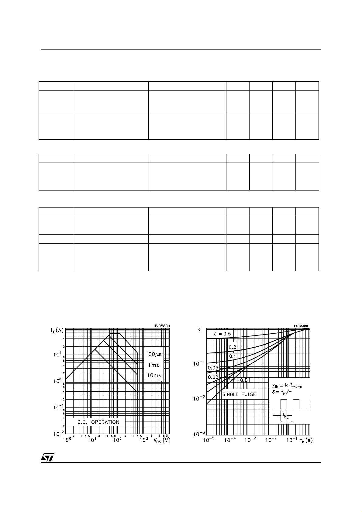
Safe Operating Area Thermal Impedance
3/8
Page 4

STW16NB60
Transfer CharacteristicsOutput Characteristics
Transconductance
Gate Charge vs Gate-so urc e V oltage
Static Drain-source On Resistance
Capacitance Variations
4/8
Page 5

Source-drain Diode Forward Characteristics
STW16NB60
Normalized On Resistance vs TemperatureNormalized Gate Thereshold Voltage vs Temp.
5/8
Page 6

STW16NB60
Fig. 2: Unclamped Inductive WaveformFig. 1: Unclamped Inductive Load Test Circuit
Fig. 3: Switching Times Test Circuit For
Resistive Load
Fig. 5: Test Circuit For Induct ive Load Switching
And Di ode Recovery Times
Fig. 4: Gate Charge test Circuit
6/8
Page 7

TO-247 MECHANICAL DATA
STW16NB60
DIM.
A 4.85 5.15 0.19 0.20
D 2.20 2.60 0.08 0.10
E 0.40 0.80 0.015 0.03
F 1 1.40 0.04 0.05
F1 3 0.11
F2 2 0.07
F3 2 2.40 0.07 0.09
F4 3 3.40 0.11 0.13
G 10.90 0.43
H 15.45 15.75 0.60 0.62
L 19.85 20.15 0.78 0.79
L1 3.70 4.30 0.14 0.17
L2 18.50 0.72
L3 14.20 14.80 0.56 0.58
L4 34.60 1.36
L5 5.50 0.21
M 2 3 0.07 0.11
V
V2
Dia 3.55 3.65 0.14 0.143
MIN. TYP MAX. MIN. TYP. MAX.
mm. inch
5º 5º
60º 60º
7/8
Page 8

STW16NB60
Information furnished is believed to be accurate and reliable. However, STMicroelectronics assumes no responsibility for the consequences
of use of such informa tion n or for an y infring ement of patent s or other rig hts of third part ies which may resu lt from its use . No l i cen se i s
granted by implication or otherwise under any patent or patent rights of STMicroelectronics. Specification mentioned in this publication are
subject to change without notice. This publication supersedes and replaces all information previously supplied. STMicroelectronics products
are not authorized for use as critical compo nents in life support devices or systems without express written approval of STMicroelectronics.
Australia - Brazil - China - Finland - France - Germany - Hong Kong - India - Italy - Japan - Malaysia - Malta - Morocco -
The ST logo is a trademark of STMicroelectronics
© 2000 STMicroelectronics – Printed in Italy – All Rights Reserved
STMicroelectronics GROUP OF COMPANIES
Singapore - Spain - Sweden - Switzerland - United Kingdom - U.S.A.
http://www.st.com
8/8
 Loading...