

Page 1
RGB HIGH VOLTAGE VIDEO AMPLIFIER
■ Bandwidth : 6MHz typical
■ Supply Voltage : 200V typical
■ Rise and Fall Time : 60ns TYPICAL
■ CRT Cathode Current Outputs for Parallel or
Sequential Cut-off or Drive Adjustment
■ Flashover Protection
DESCRIPTION
The STV5111 includes three video amplifiers
desi-gned with a high voltage bipolar/CMOS/
DMOS technology (BCD). It drives directly the
three cathodes and is protected against
flashovers. Thanks to its three cathode current
outputs, the STV5111 c an be used with both parallel and sequential sampling applications.
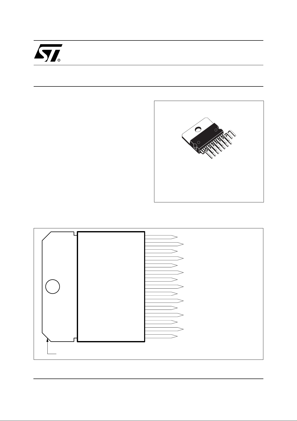
STV5111
MULTIWA TT 15
(Plastic Package)
ORDER CODE: STV5111
Figure 1. PIN CONNECTIONS
Tab connected to Pin 8
15
14
13
12
11
10
BLUE FEEDBACK
BLUE CATHODE CURRENT
BLUE OUTPUT
GREEN FEEDBACK
GREEN CATHODE CURRENT
GREEN OUTPUT
9
8
7
6
5
4
3
2
1
RED FEEDBACK
GROUND
RED OUTPUT
RED CATHODE CURRENT
V HIGH VOLTAGE
DD
RED INPUT
GREEN INPUT
V LOW VOLTAGE
CC
BLUE INPUT
5111-01 .eps
September 2003 1/7
1
Page 2
STV5111
PIN FUNCTION
N° Function Description
1 Blue Input Input of the “blue” amplifier. It is a virtual ground with 2.5V bias voltage and 75µA
input bias current.
2 V
CC
3 Green Input Input of the “green” amplifier. It is a virtual ground with 2.5V bias voltage and 75µA
4 Red Input Input of the “red” amplifier. It is a virtual ground with 2.5V bias voltage and 75µA input
5 V
DD
6 Red Cathode Current Provides the video processor with a copy of the DC current flowing into the red
7 Red Output Output driving the red cathode. Pin 7 is internally protected against CRT arc
8 Ground Also connected to the heatsink.
9 Red Feedback Output driving the feedback resistor network for the red amplifier.
10 Green Output Output driving the green cathode. Pin 10 is internally protected against CRT arc
11 Green Cathode Current Provides the video processor with a copy of the DC current flowing into the green
12 Green Feedback Output driving the feedback resistor network for the green amplifier.
13 Blue Output Output driving the blue cathode. Pin 13 is internally protected against CRT arc
14 Blue Cathode Current Provides the video processor with a copy of the DC current flowing into the blue
15 Blue Feedback Output driving the feedback resistor network for the blue amplifier.
Low voltage power supply, typically 9V.
input bias current.
bias current.
High voltage power supply, typically 200V.
cathode, for automatic cut-off or gain adjustment. If this control is not used, Pin 6
must be grounded.
discharges by a diode limiting the output voltage to V
discharges by a diode limiting the output voltage to V
DD
DD
.
.
cathode, for automatic cut-off or gain adjustment. If this control is not used, Pin 11
must be grounded.
discharges by a diode limiting the output voltage to V
DD
.
cathode, for automatic cut-off or gain adjustment. If this control is not used, Pin 14
must be grounded.
2/7
1
Page 3
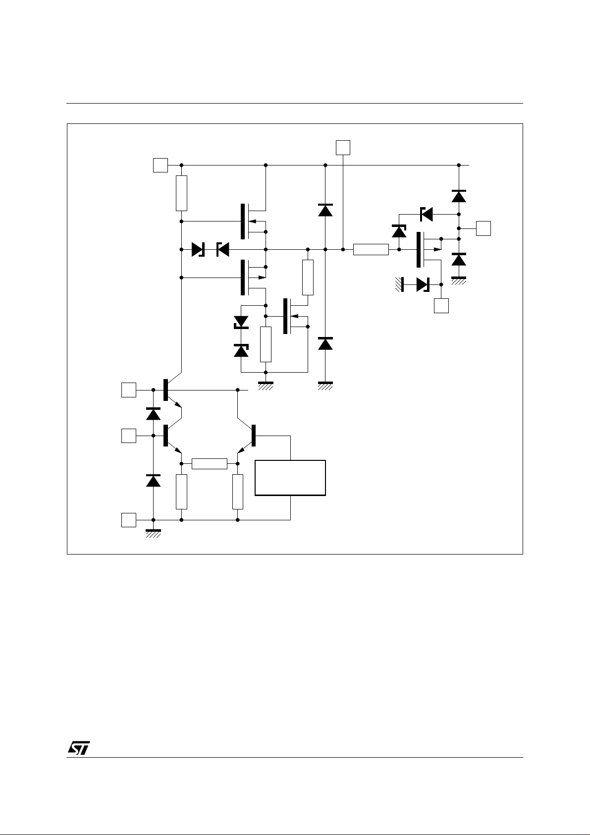
Figure 2. BLOCK DIAGRAM OF EACH CHANNEL
)
5
15
STV5111
(12, 9)
13
(10, 7
14
(11, 6)
GND
2
1
(3, 4)
8
REFERENCE
VOLTAGE
5111-02.eps
3/7
1
Page 4

STV5111
ABSOLUTE MAXIMUM RATINGS
Symbol Parameter Value Unit
V
DD
V
CC
I
OD
I
OG
I
FD
I
FG
I
T
T
oper
T
stg
THERMA L D ATA
Symbol Parameter+ Value Unit
R
(j-c) Junction-Case Thermal Resistance Max. 3 °C/W
th
(j-a) Junction-Ambient Thermal Resistance Typ. 35 °C/W
R
th
Supply High Voltage Pin 5 250 V
Supply Low Voltage Pin 2 20 V
Output Current
to V
DD
to Ground
Output Current < 50µs duration
to V
DD
to Ground
Input Current Pins 1 - 3 - 4 60 mA
j
Junction Temperature 150 °C
j
Pins 7 - 10 - 13
Protected
8
Pins 9 - 12 - 15
45
45
Operating Ambient Temperature 0, + 70 °C
Storage Temperature - 20, + 150 °C
mA
mA
mA
ELECTRICAL CHARACTERISTICS (
V
CC
= 12V ; V
= 210V ; T
DD
amb
oC
= 25
; AV = 55 unless otherwise specified)
Symbol Parameter Test Conditions Min. Typ. Max. Unit
V
DD
V
CC
I
DD
I
CC
V
sath
R
ON
High Supply Voltage (Pin5) 200 210 V
Low Supply Voltage (Pin 2) 7.5 9 10 V
High Voltage Supply Internal DC Current
(without current due to the feedback network)
V
OUT
= 100V
9.5 15 mA
Low Voltage Supply Internal DC Current 38 55 mA
Output Saturation Voltage (High level)
(Pins7-10-13)
Output Mos Transistor (Low level)
(Pins7-10-13)
IO = - 10µA
5V
1.7 k
Measured on CRT cathodes.
BW Bandwidth at - 3dB
(C
V
LOAD
OUT
= 10pF, R
= 100V, D V
PROTECT
OUT
= 1k
= 100VPP)
Ω
6MHz
Measured between 10% & 90% of
t
, t
R
F
G
O
Rise & Fall Time
Open Loop Gain 47 50 dB
Open Loop Gain Difference between
2channels
output pulse
(C
= 10pF, R
LOAD
= 100V, D V
V
OUT
PROTECT
= 100V
OUT
= 1k
Ω
PP
60 ns
-1.5 0 1.5 dB
Open Loop Gain Temperature Coefficient 0 dB/
= 2MHz, 70VPP sine wave,
V
OUT
V
= 170V, CL = 20pF
BLACK
= 68k
R
Ω
F
= 100V 2.3 2.5 2.7 V
OUT
3.6 dB/°C
V
P
REF
Internal Power Dissipation
(seecalculationbelow)
Internal Voltage Reference (Pins 1-3-4) V
Voltage Reference Temperature Coefficient 0 mV/°C
I
IB
R
Input Bias Current (Pins 1-3-4) V
Input Resistance 4k
I
= 100V 75
OUT
ESD ESD Human Body Model 1.2 kV
Ω
o
C
A
µ
Ω
4/7
1
Page 5

TYPICAL APPL ICATION
The STV5111 is composed of t hree independent
amplifiers, each of them including :
– A differential amplifier, the gain of which is fixed
by external feedback resistors,
– A voltage reference,
– A PMOS transistor providin g a copy of the cath-
ode current,
– A protection diode against CRT arc discharges.
PC Board La y ou t
The best performanc es of the high vol tage video
amplifier will be obtained only with a carefully designed PC board. Output to input capacitance is of
particular importance.
For a single amplifier, the input-output capacitance, in parallel with the relatively high feedback
resis-tance, creates a pole in the closed-loop
transfer function.
A low parasitic capacitance (0.3pF) feedback resistor and HF isolated printed wires are necessary.
Figure 3. Application Example
STV5111
Furthermore, capacitive coup ling from the output
of an amplifier toward the input of another one may
induce excessive cross-talk.
Power Dissipation
The power dissipation consists of a static part and
a dynamic part. The static dissipation is a function
of V
mation of the static power can be calculated by the
following equation:
The dynamic dissipation depends on the signal
spectrum, V
For a sine wave, dynamic dissipation is
P
The load capacitance C
capacitance (10pF), and a mplifier output capacitance (8pF) : total C
(DC), VDD and RF. Reasonable approxi-
OUT
3V
DDVDDVOUT
-----------------------------------------------
Ps
OUT
= 3 x F x CL x V
d
–()
40K
, VDD and the load capacitance.
OPP
value is about 20pF.
L
3V
OUTVDDVOUT
--------------------------------------------------+=
x 0.8 x VDD.
includes CRT and board
L
–()
R
F
VCC 9V
100
V
200V
V
DD
V
DD
V
DD
STV5111
100nF
9
7
6
12
10
11
15
13
14
F
m
1.2k
1.8k
100nF
2
8 5
W
68k
4
W
W
V
REF
3
1
470pF
W
470
4.7k
DD
10
F
m
1k
W
CATHODE 1
W
CATHODE 2
CATHODE 3
CUT-OFF
SAMPLING
5111-03.eps
5/7
1
Page 6

STV5111
PACKAGE MECHANICAL DATA
15 PINS - PLASTIC MULTIWATT
Figure 4. 15-Pin Package
6/7
1
Page 7

STV5111
Information furnished is believed to be accurate and reliable. However, STMicroelectronics assumes no responsibility for the consequences
of use of such information nor for any infringement of patents or other rights of third parties which may result from its use. No license is granted
by implic ation or otherwise under any patent or patent r i ght s of STMi croelectr oni cs. Spec i fications mentione d i n this publicatio n are subj ect
to change without notice. This publication supersedes and replaces all information previously supplied. STMicroelectronics product s are not
authorized for use as cri tical comp onents in lif e support devi ces or systems without the express written appr oval of STMic roelectronics.
The ST logo is a registered trademark of STMicroelectronics
2003 STMicroelectronics - All Rights Reserved.
Purchase of I
Australi a - Brazil - China - Finland - France - Germany - Hong Kong - India - Italy - Japan - Malaysia - Malt a - Mo rocco - Singa pore - Spain
2
C Components by STMicroelectronics conveys a license under the Philips I2C Patent. Rights to use the se components in an
2
I
C system i s granted pro vi ded that the sy stem conforms to the I2C Standard Specification as defined by Philips.
STMicroelectronics Grou p of Companies
Sweden - Switzerland - United K i ngdom - U.S.A.
http://www.s t. com
7/7
 Loading...