

Page 1
STV40NE03L-20
N - CHANNEL 30V - 0.014Ω - 40A - PowerSO-10
STripFET MOSFET
TYPE V
DSS
R
DS(on)
I
D
ST V40NE03L-20 30 V < 0.020 Ω 40 A
■ TYPICALR
■ EXCEPTIONAL dv/dt CAPABILITY
■ LOW GATE CHARGE A 100
■ APPLICATIONORIENTED
DS(on)
= 0.014 Ω
o
C
CHARACTERIZATION
DESCRIPTION
This PowerMOSFET is the latest developmentof
STMicroelectronics unique ”Single Feature
Size” strip-based process. The resulting
transistor shows extremely high packing density
for low on-resistance, rugged avalanche
characteristics and less critical alignment steps
therefore a remarkable manufacturing
reproducibility.
APPLICATIONS
■ HIGHCURRENT, HIGH SPEEDSWITCHING
■ SOLENOIDAND RELAYDRIVERS
■ MOTORCONTROL, AUDIOAMPLIFIERS
■ DC-DC& DC-ACCONVERTERSIN HIGH
PERFORMANCE VRMs
■ AUTOMOTIVE ENVIRONMENT(INJECTION,
ABS, AIR-BAG, LAMPDRIVERS,Etc.)
10
1
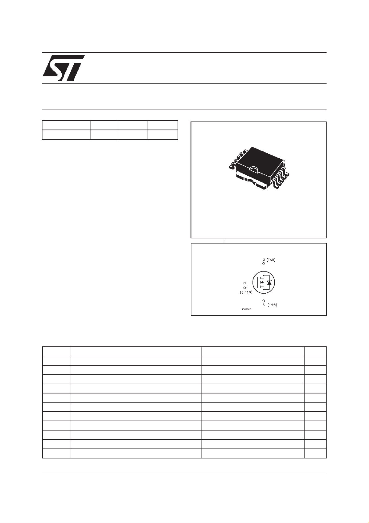
PowerSO-10
INTERNAL SCHEMATIC DIAGRAM
ABSOLUTE MAXIMUM RATINGS
Symbol Parameter Value Uni t
V
V
V
I
DM
P
dv/ dt (
T
(•) Pulse width limited by safe operating area (1)ISD≤ 40 A, di/dt ≤300 A/µs, VDD≤ V
May 2000
Drain-source Voltage (VGS=0) 30 V
DS
Drain- g at e V olt age (RGS=20kΩ)30V
DGR
Gate-source Voltage
GS
I
Drain Cur rent (c ont in uous ) at Tc=25oC40A
D
I
Drain Cur rent (c ont in uous ) at Tc=100oC28A
D
20 V
±
(•) Drain Current (pulsed) 160 A
Total Dissipation at Tc=25oC80W
tot
Derat ing F ac tor 0.53 W/
1 ) Peak Diode Recovery voltage slope 7 V / ns
Sto rage Temperatur e -65 to 175
stg
T
Max. Operating J unction Temper at ur e 175
j
(BR)DSS,Tj≤TJMAX
o
C
o
C
o
C
1/8
Page 2
STV40NE03L-20
THERMAL DATA
R
thj-case
R
thj-amb
R
thc-sink
T
AVALANCHE CHARACTERISTICS
Symbol Parameter Max Value Unit
I
AR
E
Ther mal Resistanc e Junct ion-case Max
Ther mal Resistanc e Junct ion-ambient Max
Ther mal Resistanc e Case-sink Ty p
Maximum Lead Temperatu r e For Soldering Purpose
l
Avalanche Current, Repetitive or Not-Repetitive
(pulse width limited by T
Single Pul se Avalanche Ener gy
AS
(starting T
=25oC, ID=IAR,VDD=15V)
j
max,δ <1%)
j
1.88
62.5
0.5
300
40 A
200 mJ
o
C/W
o
C/W
o
C/W
o
C
ELECTRICAL CHARACTERISTICS
= -40to 150oC unlessotherwisespecified)
(T
J
OFF
Symbol Parameter Test Conditions Min. Typ. Max. Unit
V
(BR)DSS
I
DSS
I
GSS
Drain-source
Break dow n Vo lt age
Zero Gate Voltage
Drain Curre nt (V
GS
Gat e- bod y Leakag e
Current (V
DS
=0)
ID=250µAVGS=0 Tc=25oC
=250µAVGS=0
I
D
V
=MaxRating Tc=25oC
=0)
DS
=MaxRating
V
DS
= ± 20 V ± 100 nA
V
GS
30
27
1
50
ON(∗)
Symbol Parameter Test Conditions Min. Typ. Max. Unit
V
GS(th)
R
DS(on)
I
D(on)
Gate Threshold Voltage VDS=VGSID= 250 µ ATc=25oC
V
DS=VGSID
Sta t ic Drain-s our c e On
Resistance
VGS=10V ID=20A Tc=25oC
=5V ID=20A Tc=25oC
V
GS
V
=10V ID=20A
GS
=5V ID=20A
V
GS
On State Drain Current VDS>I
D(on)xRDS(on )max
= 250 µ A
1
0.6
1.8 2.5
3.0
0.014 0. 0 2
0.023
0.04
0.046
20 A
VGS=10V
DYNAMIC
V
µA
µ
V
V
Ω
Ω
Ω
Ω
A
Symbol Parameter Test Conditions Min. Typ. Max. Unit
g
(∗)Forward
fs
VDS>I
D(on)xRDS(on )maxID
=20A 10 S
Tr ansc on duc tance
C
C
C
Input Capaci t ance
iss
Out put Capac itance
oss
Reverse Transfer
rss
VDS=25V f=1MHz VGS= 0 1850
450
160
2400
590
210
Capacit a nc e
2/8
pF
pF
pF
Page 3
STV40NE03L-20
ELECTRICAL CHARACTERISTICS
(continued)
SWITCHING ON
Symbol Parameter Test Conditions Min. Typ. Max. Unit
t
d(on)
Q
Q
Q
Turn-on Time
Rise Time
t
r
Tot al Gate Charge
g
Gat e- Source Char g e
gs
Gate-Drain Charge
gd
VDD=15V ID=20A
R
G
=4.7
Ω
VGS=5V
25
16033210
VDD=24V ID=40A VGS=5V 29
12
14
38 nC
SWITCHING OFF
Symbol Parameter Test Conditions Min. Typ. Max. Unit
t
r(Voff)
t
t
Off-volt age Rise Time
Fall T ime
f
Cross-over Tim e
c
VDD=24V ID=40A
R
G
=4.7
Ω
VGS=5V
25
120
155
33
160
210
SOURCEDRAIN DIODE
Symbol Parameter Test Conditions Min. Typ. Max. Unit
I
SD
I
SDM
V
SD
t
Q
I
RRM
(∗) Pulsed:Pulse duration = 300µs, duty cycle 1.5%
(•) Pulse width limited by safeoperating area
Source-drain Current
(•)
Source-drain Current
40
160
(pulsed)
(∗)ForwardOnVoltage ISD=40A VGS=0 1.5 V
Reverse Recovery
rr
Time
Reverse Recovery
rr
ISD= 40 A di/dt = 100 A/µs
=20V Tj= 150oC
V
DD
50
0.9
Charge
Reverse Recovery
3.5
Current
ns
ns
nC
nC
ns
ns
ns
A
A
ns
µ
A
C
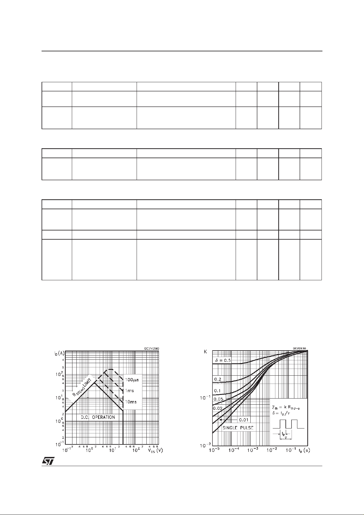
SafeOperating Area ThermalImpedance
3/8
Page 4

STV40NE03L-20
OutputCharacteristics
Transconductance
TransferCharacteristics
Static Drain-sourceOn Resistance
Gate Charge vs Gate-sourceVoltage
4/8
CapacitanceVariations
Page 5

STV40NE03L-20
NormalizedGate ThresholdVoltage vs
Temperature
Source-drainDiode Forward Characteristics
NormalizedOn Resistancevs Temperature
5/8
Page 6

STV40NE03L-20
Fig. 1:
UnclampedInductiveLoad TestCircuit
Fig. 3: SwitchingTimes Test Circuits For
ResistiveLoad
Fig. 2:
UnclampedInductiveWaveform
Fig. 4: Gate Charge test Circuit
Fig. 5:
Test Circuit For InductiveLoad Switching
And Diode Recovery Times
6/8
Page 7

PowerSO-10 MECHANICAL DATA
STV40NE03L-20
DIM.
mm inch
MIN. TYP. MAX. MIN. TYP. MAX.
A 3.35 3.65 0.132 0.144
A1 0.00 0.10 0.000 0.004
B 0.40 0.60 0.016 0.024
c 0.35 0.55 0.013 0.022
D 9.40 9.60 0.370 0.378
D1 7.40 7.60 0.291 0.300
E 9.30 9.50 0.366 0.374
E1 7.20 7.40 0.283 0.291
E2 7.20 7.60 0.283 0.300
E3 6.10 6.35 0.240 0.250
E4 5.90 6.10 0.232 0.240
e 1.27 0.050
F 1.25 1.35 0.049 0.053
H 13.80 14.40 0.543 0.567
h 0.50 0.002
L 1.20 1.80 0.047 0.071
q 1.70 0.067
α 0
o
o
8
==
==
HE
h
A
F
A1
610
51
eB
M
0.25
D
==
D1
==
DETAIL”A”
E2
==
DETAIL”A”
Q
B
0.10 A
E1E3
==
SEATING
PLANE
A
C
α
B
E4
==
SEATING
PLANE
A1
L
==
0068039-C
7/8
Page 8

STV40NE03L-20
Information furnished is believed to be accurate and reliable. However, STMicroelectronics assumes no responsibility for the consequences
of use of such information nor for any infringement of patents or other rights of third parties which may result from its use. No license is
granted by implication or otherwise under any patent or patent rights of STMicroelectronics. Specification mentioned in thispublication are
subject to change withoutnotice. Thispublication supersedes and replaces allinformation previously supplied. STMicroelectronics products
are not authorized for use as critical components inlife support devices or systems without express written approval ofSTMicroelectronics.
The ST logo is a trademarkof STMicroelectronics
2000 STMicroelectronics – Printedin Italy – All Rights Reserved
STMicroelectronics GROUP OF COMPANIES
Australia - Brazil -China - Finland- France - Germany - Hong Kong - India - Italy- Japan - Malaysia - Malta - Morocco -
Singapore - Spain - Sweden -Switzerland - United Kingdom - U.S.A.
http://www.st.com
8/8
 Loading...