

Page 1
FOR AUDIO AND VIDEO A PPLICATIONS
.
TWO TIMING AND DATA FORMAT MODES
.
7 SUB-SYSTEM ADDR ESSES
.
UP TO 64 COMMANDS PER SUB-SYSTEM
ADDRESS
.
KEY RELEASE DETECTION BY TOGGLE BIT
(1 toggle bit in mode A and 2 toggle bits in
mode B)
.
HIGH CURRENT RE MO T E OUTPUT
AT V
.
VERY LOW STA ND-B Y CU RRENT (< 2µA)
.
1mA OPERATIONAL CURRENT AT 6V SUPPLY
.
CERAMIC RESONATOR CONTROLLED
FREQUENCY (typ. 450kHz)
.
MODULATED TRANSMISSION
.
SUPPLY VOLTA G E RANGE 2V TO 6.5V
.
LOW NUMBER OF EXTERNAL COMPONENTS
= 3V (-IOH = 80mA)
DD
STV3012
REMOTE CONT R OL TRANSMITTER
PRELIMINARY DATA
DIP20
(Plastic Package)
ORDER CODE : STV3012
PIN CONNECTIONS
REMO
SEN6N
SEN5N
SEN4N
SEN3N
SEN2N
DESCRIPTION
The STV3012 is a general purpose infrared rem ote
control transmitter system for low voltage supply
applications. It is able to generate a total number
of 448 commands which are divided into 7 sub-sys tem groups with 64 commands each. The sub-system code may be selected by a press button, a
slider switch or hard wired. T wo different timing and
data format modes are available.
March 1993
This is advance information on a new product now in development or undergoing evaluation. Details are subject to change without notice.
SEN1N
SEN0N
ADRM
V
1
2
3
4
5
6
7
8
9
10
SS
V
20
19
18
17
16
15
14
13
12
11
DD
DRV6N
DRV5N
DRV 4N
DRV 3N
DRV 2N
DRV1N
DRV0N
OSCO
OSCI
3012-01.EPS
1/8
Page 2
STV3012
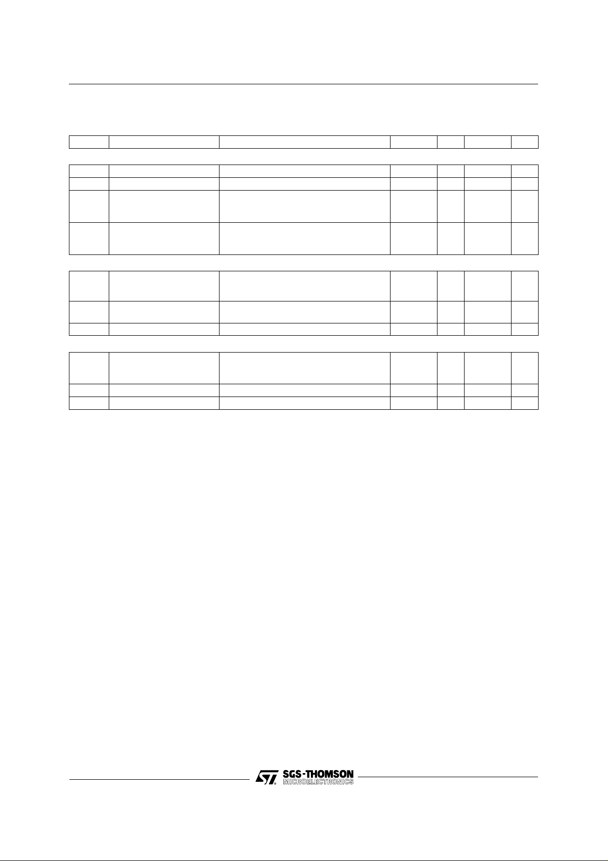
BLOCK DIAG RAM
OSCO
OSCI
SEN6N
SEN5N
SEN4N
SEN3N
SEN2N
SEN1N
SEN0N
REMO
12
OSCILLATOR
2
3
4
5
6
7
8
1
ENCODER
KEYBOARD
REMOTE
DIVIDER
LATCHES
ADDRESS
PARALLEL
/SERIAL
CONVERTER
MASTER
CLEAR
SYST.
CONTR
DRIVER
KEYBOARD
DECODER
20
1011
9
19
18
17
16
15
14
13
V
DD
V
SS
ADRM
DRV6N
DRV5N
DRV4N
DRV3N
DRV2N
DRV1N
DRV0N
ABSOLUTE MAXIMUM RATINGS
Symbol Parameter Value Unit
- I
V
DD
V
V
O
± I
(REMO)
P
tot
T
stg
T
oper
Supply Voltage - 0.3, 7.0 V
Input Voltage - 0.3, VDD + 0.3 V
I
Output Voltage - 0.3, VDD + 0.3 V
D.C. Current into any input or output 10 mA
Peak REMO Output Current during 10µs, duty factor = 1%
Power Dissipation per package for T
= - 20 to + 70oC 200 mW
amb
300 mA
Storage Temperature - 55, + 125
Operating Ambient Temperature -20, + 70
3012-02.EPS
o
C
o
C
3012-01.TBL
ELECTRICAL CHARACTERISTICS
V
= 0V, TA = 25oC (unless otherwise specified)
SS
Symbol Parameter Test Conditions Min. Typ. Max. Unit
V
I
f
OSC
KEYBOARD MATRIX - Inputs SEN0N to SEN6N
V
V
- I
KEYBOARD MATRIX - Outputs DRV0N to DRV6N
V
2/8
Supply Voltage TA = 0 to + 70oC26.5V
DD
Supply Current • Active f
DD
REMO Output unload VDD = 6V
• Inactive (stand-by mode) V
= 455kHz VDD = 3V
OSC
0.25
1.0
= 6V 2
DD
0.5
2
Oscill. Frequency VDD = 2 to 6.5V (ceramic resonator) 350 600 kHz
Input Voltage Low VDD = 2 to 6.5V 0.3 x V
IL
Input Voltage High VDD = 2 to 6.5V 0.7 x V
IH
Input Current VDD = 2V, VI = 0V
I
Input Leakage Current VDD = 6.5V, VI = V
I
I
Output Voltage "ON" VDD = 2V, IO = 0.1mA
OL
I
Output Current "OFF" VDD = 6.5V, VO = 6.5V 10
O
= 6.5V, VI = 0V
V
DD
DD
VDD = 6.5V, IO = 1.0mA
DD
10
100
DD
100
600
1
0.3
0.6
mA
mA
µA
V
V
µA
µA
µA
V
V
µA
3012-02.TBL
Page 3
STV3012
ELECTRICAL CHARACTERISTICS
T
= 25oC, unless otherwise specified
amb
Symbol Parameter Test Conditions Min. Typ. Max. Unit
CONTROL INPUT ADRM
Input Voltage Low 0.3 x V
V
IL
V
Input Voltage High 0.7 x V
IH
I
Input Current Low
IL
(switched P and N
channel pull-up/pull down)
I
Input Current High
IH
(switched P and N
channel pull-up/pull down)
DATA OUTPUT REMO
- I
OSCILLATOR
V
V
Output Current High VDD = 2.5V, VOH = 0.8V, TA = 70oC
OH
I
Output Current Low VDD = 2V, VOL = 0.4V
OL
t
Pulse Length VDD = 6.5V, Oscill. Stopped 1 msec
OH
Input Current OSCI at V
I
I
Output Voltage high VDD = 6.5V, - IOH = 0.1mA VDD - 0.8 V
OH
Output Voltage Low VDD = 6.5V, IOL = 0.1mA 0.7 V
OL
Pull-up Act. Oper. Condition, VIN = V
Pull-down Act. Stand-by Cond.,VIN = V
VDD = 2.5V, VOH = 0.8V, TA = 25oC
V
DD
VDD = 6.5V, VOL = 0.4V
VDD = 2V
VDD = 6.5V
VDD = 2V
VDD = 6.5V
= 6.5V, VOH = 5V
DD
VDD = 2V
= 6.5V 5
V
DD
SS
DD
DD
-10
-100
10
100
70
80
80
0.6
0.6
DD
-100
-600
100
600
5
7
V
V
µA
µA
µA
µA
mA
mA
mA
mA
mA
µA
µA
3012-03.TBL
I - INPUTS AND OUTP UT S
I.1 - Key Matrix Inputs and Outp uts (DRV 0N to
DRV6N and SEN0N to SEN6N)
The transmitter k eyboard is arranged as a scanned
matrix. The matrix consists of 7 driver ouputs a nd
7 sense inputs. The driver outputs DRV0N to
DRV6N are open drain N-channel transistors and
they are conductive in the stand-by mode. The 7
sense inputs (SEN0N to SEN6N) enable the generation of 56 command codes. With 2 external
diodes all 64 commands are addressable. The
sense inputs have P-channel pull- up transistors so
that they are HIGH until they are pulled LOW by
connecting them to an output via a key depression
to initiate a code transmission. The cod es for the
selected key are given in Table 1.
I.2 - Address Mode Input (ADRM)
The sub-system address and the transmission
mode are defined by connecting the ADRM input
to one or more driver outputs (DRV0N to DRV6N)
of the key matrix. If more than one driver is connected to ADRM, they must be decoupled by diodes. This allows the definition of seven
sub-system address es as shown in Table 2.
The ADRM input has switched pull-up and pulldown loads. In the stand-by mode only the pull-
down device is active. Whether ADRM is open
(sub-system address 0) or connected to the driver
outputs, this input is LOW and will not cause unwanted dissipation. W hen the transmitter becomes
active by pressing a key, the pull-down device is
switched-off and the Pull-up device is switched-on,
so that the applied driver signals are sensed for the
decoding of the sub-syst em address and the mode
of transmission.
The arrangement of the sub-system address coding is such that only the driver DRVnN with the
highest number (n) defines the sub-system address, e.g. in mode B, if drivers DRV 2N and DRV4N
are connected to ADRM, only DRV4N will define
the sub-system addre ss. This option can be used
in systems requiring more than one sub-system
address. The transmitt er may be hard-wir e for subsystem address 2 by connecting DRV1N to ADRM.
If now DRV3N is added to ADRM by a key or a
switch, the transmitted sub-system address
changes to 4. A change of the sub-system will not
start a transmission.
I.3 - Remote Control Signal Output (REMO)
The REMO signal output stage is a push-pull type.
In the HIGH state, a bipolar emitter-follower allows
a high output current. The timing of the data output
format is listed in Figures 1 and 2.
3/8
Page 4

STV3012
The information is defined by the first edge of the
modulated pulses. During mode A, the data word
starts with the four bits for defining the sub-system
address S3, S2, S1 and S0, followed by the toggle
bit T0, and seven bits G, F, E, D, C, B and A, which
are defined by the selected key. During mode B,
the data word starts with the Toggle bit s T1 and T0,
followed by three bits for defining the sub-system
address S2, S1 and S0, and six bits F, E, D, C, B
and A which are defined by the selected key.
Table 1 : Key Codes
Matrix
Drive
DRV0N
DRV1N
DRV2N
DRV3N
DRV4N
DRV5N
DRV6N
V
SS
DRV0N to V
DRV0N to V
DRV0N to V
DRV0N to V
DRV0N to V
DRV0N to V
DRV0N to V
* The C, B and A codes are identical to SEN0N as given above.
** Bit position G only available in mode A.
SS
SS
SS
SS
SS
SS
SS
Matrix
Sense
SEN0N
SEN0N
SEN0N
SEN0N
SEN0N
SEN0N
SEN0N
SEN0N
G**FEDCBA
0
0
0
0
0
0
0
0
SEN1N 0 0 0 1 * 8 to 15
SEN2N 0 0 1 0 * 16 to 23
SEN3N 0 0 1 1 * 24 to 31
SEN4N 0 1 0 0 * 32 to 39
SEN5N 0 1 0 1 * 40 to 47
SEN6N 0 1 1 0 * 48 to 55
SEN5N and SEN6N 0 1 1 1 * 56 to 63
The toggle bits function as an indication for the
decoder that the next instruction has t o be consi dered as a new com mand.
The REMO output is protected against "lock-up",
i.e. the length of an output pulse is limited to
< 1msec, even if the oscillator stops during an
output pulse. This avoids the rapid discharge of the
battery that would otherwise be caused by the
continuous activation of the LED.
Code
0
0
0
0
0
0
0
0
0
0
0
0
0
0
0
0
0
0
0
0
0
0
0
0
0
0
1
0
1
0
1
0
1
0
0
1
1
0
1
1
0
0
0
1
1
0
1
1
Matrix
Position
0
1
2
3
4
5
6
7
3012-05.TBL
Table 2 : Transmission Mode and S ub-sy stem A ddress Selection
Mode Sub-system Address Driver DRVnN for n =
#S3S2S1S00123456
M
O
D
E
A
M
O
D
E
B
O = connected to ADRM
blank = not connected to ADRM
X = don’t care
The sub-system address and the transmission mode are defined by connecting the ADRM input to one or more driver outputs (DRV0N to
DRV6N) of the key matrix. If more than one driver is connected to ADRM, they must be decoupled by diodes.
00000
10010XXXXXO
20110XXXXO
30001XXXO
40101XXO
50011XO
60111O
0111 O
1000O O
2001XO O
3010XXO O
4 011XXXO O
5 100XXXXO O
6 101XXXXXOO
3012-04.TBL
4/8
Page 5

STV3012
Figure 1 : Data Format of REMO ; T0 and T1 = toggle bits ; S0, S1, S2 and S3 = sub-system address ;
A, B, C, D, E, F and G = command bits
MODE A
H
REMO
L
bit
data
MODE B
REMO
bit
data
S30S2
11
H
L
T0
T1
0
S0
S1
0
S20S1
11
Bit Separation (tB) Mode A Mode B
Logic "0" 1 x t
Logic "1" 2 x t
Toggle bit time 1 x t0 or 2 x t
Figure 2 : Pulse Train Timing (ref. to f
t
(bit duration)
B
t
PW
t
M
t
t
MH
ML
T0 F
G
1
0
1
= 400kHz)
OSC
t
w
0E0D1C0B0
t
w
B
C
D
ES00F
1
0
0
0
0
0
A
00
A
1
2 x t
3 x t
2 x t0 or 3 x t
S3
T0
3012-03.EPS
0
0
0
1st bit 2nd bit last bit
tW(word distance)
Mode t0 (ms)
(µs) tMH (µs) tML (µs)
t
M
t
A 2.52 30 10 20 86.04
B 2.88 30 10 20 138
Mode A and B
t
OSC
t
t
t
ML
MH
2.5µs
M
12 x t
8 x t
4 x t
OSC
OSC
OSC
oscillation period
modulation period
modulation period LOW
modulation period HIGH
Mode A
t
PW
t
t
0
W
(15 x tM) + t
1008 x t
OSC
34416 x t
MH
OSC
modulated pulse
basic unit of pulse distance
word distance
Mode B
t
PW
t
t
0
W
(11 x tM) + t
1152 x t
OSC
55296 x t
MH
OSC
modulated pulse
basic unit of pulse distance
word distance
(ms)
W
3012-04.EPS
5/8
Page 6

STV3012
I.4 - Oscillator Input and Output
The external components must be connected to
these pins when using an oscillator with a c eramic
resonator. The oscillator frequency may vary between 350kHz and 600kHz as defined by the resonator . No external feedback resist or is allowed.
II - FUNCTIONAL DESCRIPTION
Key operation (see Figure 3) :
In the stand-by mode all drivers (DRV0N to
DRV6N) are on (low impedance to V
). Whenever
SS
a key is pressed, one or more of the sense inputs
(SENnN) are tied to ground. This will start the
power-up sequence. First the oscillator is activat ed
and after the debounce time t
the output drivers
DB
(DRV0N to DRV6N) becom e active suc ces sively.
Within the firs t scan c ycle, the trans miss ion mode,
the applied sub-system addre ss and the selected
command code are sensed and loaded into an
internal data latch.
In contrast to the command code, the sub-system
is sensed only within the first scan cycle. If the
applied sub-system address is changed while the
Command key is pr essed, the trans mitted s ub-system address is not altered.
In a multiple key stroke sequence the command
code is always altered in accordance with the
sensed key.
III - OUTPUT SEQUENCE (DATA FORMAT)
The output operation will start when the selected
code is found. A burst of pulses, including the
latched address and command codes, is generated
at the output REMO as lon g as a key is pressed.
The operation is terminated by releasing the key or
if more than one key is pressed at the same time.
Once a sequence is started, the transmitted data
words will always be completed after the key is
released.
The toggle bits T1 and T0, during mode A only T0,
toggle if the key is released for a minimum time
t
. The toggle bits remain unchanged within a
REL
multiple key-stroke sequence.
IV - MULTIPLE KEY-STROKE PROTECTION
The keyboard is protected against multiple keystrokes (Figure 4). If more than one key is pressed
at the same time, the circuit will not generate a ne w
output at REMO. In case of a multiple key-stroke,
the scan repetition rate is increased to detect the
release of a key as soon as possible.
There are two restrictions caused by the special
structure of the keyboard matrix : the keys switching to ground (code numbers 7, 15, 23, 31, 39, 47,
55 and 63) and the keys connected to SEN5N and
SEN6N are not covered completely by the multiple
key protection. If one sense input is switched to
ground, further keys on the same sense line are
ignored, i.e. the command code corresponding to
"key to ground" is transmitted. SEN5N and SEN6 N
are not protected against multiple keystroke on the
same driver line, because this condition has been
used for the definition of additional codes (code
number 56 to 63).
Figure 3 : Single Key-stroke Sequence. Debounce time : tDB = 4 to 9 x t0,
REV
DRVnN
REMO
OSCO
6/8
closed
released
off
on
H
L
H
L
Start time : t
key bouncing
scan
t
DB
t
= 5 to 10 x t0, Minimum release time : t
ST
scan scan
t
W
ST
OSCILLATOR ACTIVE
REL
= t0.
t
REL
new key
new word
3012-05.EPS
Page 7

Figure 4 : Multiple Key-stroke Sequence. Scan rate multiple key-strok e : tSM = 8 to 10 x t0.
STV3012
key bouncing
closed
KEY A
released
closed
KEY B
released
scan scan scan
off
DRVnN
on
t
DB
H
REMO
OSCO
L
t
ST
H
L
word key A word key A
TYPICAL APPL ICATION
key A decoded as HIGH
key A decoded as LOW
tt
t
W
SM
DB
t
ST
word key B
OSCILLATOR ACTIVE
3012-06.EPS
SEN0N
SEN1N
SEN2N
SEN3N
SEN4N
SEN5N
SEN6N
ADRM
DRV0N
13 14 15 16 17
8
7
6
5
4
3
2
9
10
V
SS
DRV2N
DRV1N
STV3012
11 12
OSCI OSCO
DRV3N
DRV5N
18 19
DRV6N
V
DD
20
REMO
1
3012-07.EPS
DRV4N
7/8
Page 8

STV3012
PACKAGE MECHANICAL DATA
20 PINS - PLASTIC DIP
I
a1
L
Z
e3
b
B
e
E
Z
D
20 11
F
110
Dimensions
Min. Typ. Max. Min. Typ. Max.
a1 0.254 0.010
B 1.39 1.65 0.055 0.065
b 0.45 0.018
b1 0.25 0.010
D 25.4 1.000
E 8.5 0.335
e 2.54 0.100
e3 22.86 0.900
F 7.1 0.280
i 3.93 0.155
L 3.3 0.130
Z 1.34 0.053
Millimeters Inches
b1
PM-DIP20.EPS
DIP20.TBL
Information furnished i s believed to be accurate and rel iabl e. However, S GS-THOMSON Microel ectroni cs assumes no responsibil ity
for the consequences of use of such information nor for any infringement of patents or other rights of third parties which may result
from its use. No licence is granted by implication or otherwise under any patent or patent rights of SGS-THOMSON Microelectronics.
Specifications mentioned in this publication are subject to change without notice. This publication supersedes and replaces all
information previously supplied. SGS-THOMSON Microelectronics products are not authorized for use as critical components in life
support devices or systems without express written approval of SGS-THOMSON Microelectronics.
© 1994 SGS-THOMSON Microelectronics - All Rights Reserved
2
Purchase of I
2
C Patent. Rights to use these components in a I2C system, is granted provided that the system conforms to
I
Australia - Brazil - China - France - Germany - Hong Kong - Italy - Japan - Korea - Malaysia - Malta - Morocco
The Netherlands - Singapore - Spain - Sweden - Switzerland - Taiwan - Thailand - United Kingdom - U.S.A.
C Components of SGS-THOMSON Microelectronics, conveys a license under the Philips
2
C Standard Specifications as defined by Philips.
the I
SGS-THOMSON Microelectronics GROUP OF COMPANIES
8/8
 Loading...