

Page 1
N-channel 24V - 0.8mΩ - 280A - PowerSO-10
Features
Typ e V
STV300NH02L 24V 0.001Ω 280A
■ R
DS(on)*Qg
■ Conduction losses reduced
■ Low profile, very low parasitic inductance
■ Switching losses reduced
industry’s benchmark
DSS
Applications
■ Switching applications
–OR-ing
■ Specially designed and optimized for high
efficiency DC/DC converters.
R
DS(on)
STV300NH02L
STripFET™ Power MOSFET
I
D
10
1
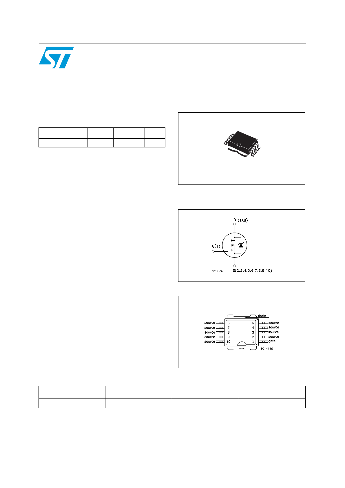
PowerSO-10
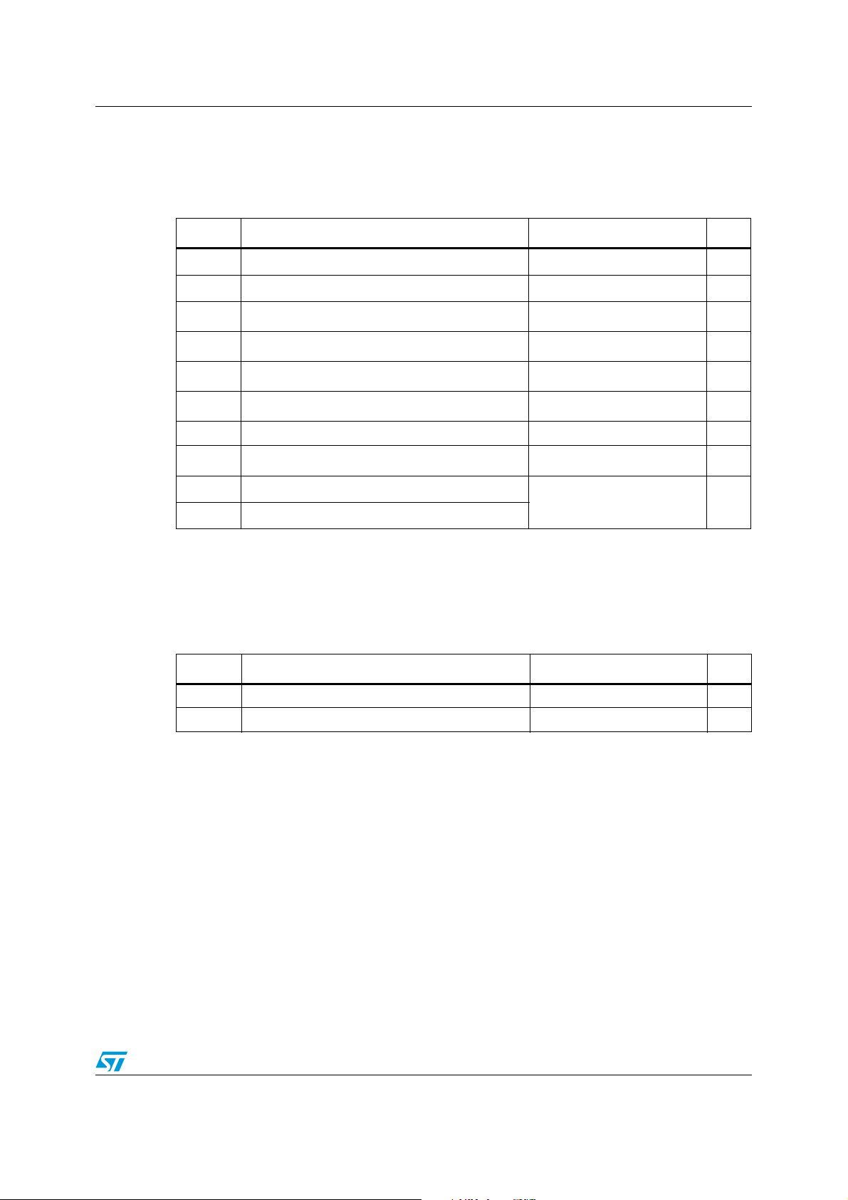
Figure 1. Internal schematic diagram
Description
This product utilizes the latest advanced design
rules of ST’s proprietary STripFET™ technology.
This is suitable for high current OR-ing
application.
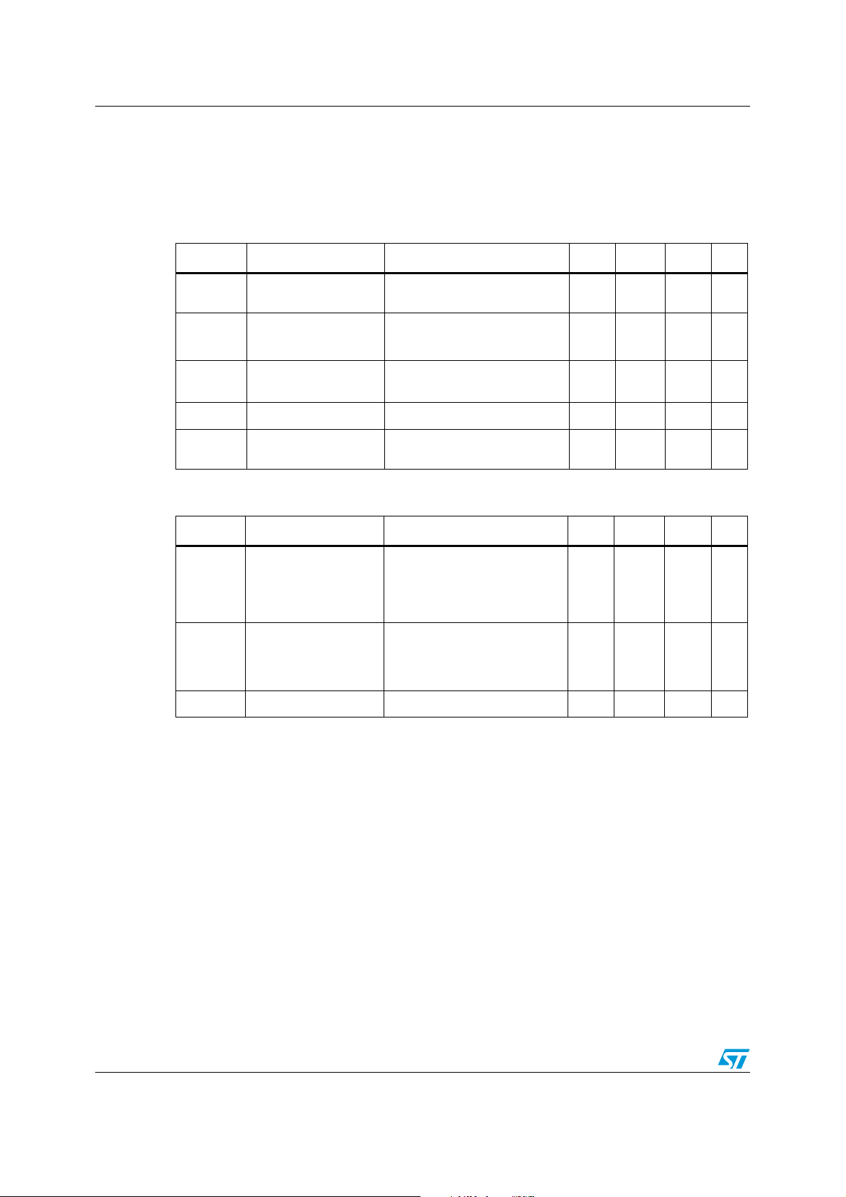
Figure 2. Connection diagram (top view)
Table 1. Device summary
Order code Marking Package Packaging
STV300NH02L 300NH02L PowerSO-10 Tape & reel
September 2007 Rev 2 1/12
www.st.com
12
Page 2

Content STV300NH02L
Content
1 Electrical ratings . . . . . . . . . . . . . . . . . . . . . . . . . . . . . . . . . . . . . . . . . . . . 3
2 Electrical characteristics . . . . . . . . . . . . . . . . . . . . . . . . . . . . . . . . . . . . . 4
2.1 Electrical characteristics (curves) . . . . . . . . . . . . . . . . . . . . . . . . . . . . . 5
3 Test circuits . . . . . . . . . . . . . . . . . . . . . . . . . . . . . . . . . . . . . . . . . . . . . . 8
4 Package mechanical data . . . . . . . . . . . . . . . . . . . . . . . . . . . . . . . . . . . . . 9
5 Revision history . . . . . . . . . . . . . . . . . . . . . . . . . . . . . . . . . . . . . . . . . . . 11
2/12
Page 3
STV300NH02L Electrical ratings
1 Electrical ratings
Table 2. Absolute maximum ratings
Symbol Parameter Value Unit
P
V
V
I
I
I
DM
TOT
D
D
Drain-source voltage (vgs = 0)
DS
Gate-source voltage ± 20 V
GS
(1)
Drain current (continuous) at TC = 25°C
(1)
Drain current (continuous) at TC = 100°C
(2)
Drain current (pulsed) 1120 A
(3)
Total dissipation at TC = 25°C
24 V
280 A
200 A
300 W
Derating factor 2 W/°C
(4)
E
AS
T
1. This value is limited by package
2. Pulse with limited by safe operating area
3. This value is rated according to Rthj-c
4. Starting Tj = 25°C, ID = 60A, VDD = 20V
Single pulse avalanche energy 1.6 J
Storage temperature
stg
T
Operating junction temperature
j
-55 to 175 °C
Table 3. Thermal data
Symbol Parameter Value Unit
Rthj-case Thermal resistance junction-case max 0.5 °C/W
Rthj-amb Thermal resistance junction-ambient max 50 °C/W
3/12
Page 4
Electrical characteristics STV300NH02L
2 Electrical characteristics
(Tcase =25°C unless otherwise specified)
Table 4. On /off states
Symbol Parameter Test conditions Min. Typ. Max. Unit
V
(BR)DSS
I
DSS
I
GSS
V
GS(th)
R
DS(on)
Drain-source
breakdown voltage
Zero gate voltage
drain current (VGS = 0)
Gate body leakage
current (V
DS
= 0)
Gate threshold voltage
Static drain-source on
resistance
= 1mA, VGS= 0
I
D
V
= Max rating,
DS
V
= Max rating, Tc=125°C
DS
= ± 20V
V
DS
V
= VGS, ID = 250µA
DS
VGS= 10V, ID= 80A
24 V
1
10µAµA
±100 nA
11.52V
0.8 1 mΩ
Table 5. Dynamic
Symbol Parameter Test conditions Min. Typ. Max. Unit
C
C
C
Q
Q
Q
R
Input capacitance
iss
Output capacitance
oss
Reverse transfer
rss
capacitance
g
Total gate charge
Gate-source charge
gs
Gate-drain charge
gd
Gate input resistance
G
= 15V, f = 1 MHz, VGS =0
V
DS
= 12V, ID= 120A,
V
DD
= 10V
V
GS
(see Figure 15)
= 0V, f = 1 MHz, VGS =0
V
DS
7055
3251
307
109
30
26
4.4 Ω
pF
pF
pF
nC
nC
nC
4/12
Page 5

STV300NH02L Electrical characteristics
Table 6. Switching times
Symbol Parameter Test conditions Min. Typ. Max Unit
= 12V, ID = 60A
V
t
d(on)
t
t
d(off)
t
Turn-on delay time
Rise time
r
Turn-off delay time
Fall ti me
f
DD
= 4.7Ω, VGS= 10V,
R
G
(see Figure 14)
V
= 12V, ID = 60A
DD
= 4.7Ω, VGS= 10V,
R
G
(see Figure 14)
18
275
138
94.4
ns
ns
ns
ns
Table 7. Source drain diode
Symbol Parameter Test conditions Min. Typ. Max. Unit
I
SD
I
SDM
V
SD
t
Q
I
RRM
t
Q
I
RRM
1. Pulsed: Pulse duration = 300 µs, duty cycle 1.5%
Source-drain current
Source-drain current (pulsed)
(1)
Forward on voltage
rr
Reverse recovery time
Reverse recovery charge
rr
Reverse recovery current
rr
Reverse recovery time
Reverse recovery charge
rr
Reverse recovery current
I
SD
I
SD
V
DD
(see Figure 19)
I
SD
V
DD
(see Figure 19)
= 120A, VGS = 0
= 120A,di/dt = 100A/µs
= 20V, Tj = 25°C
= 120A,di/dt = 100A/µs
= 20V, Tj = 150°C
63
85
2.7
63
88
2.8
280
1120AA
1.3 V
ns
nC
A
ns
nC
A
5/12
Page 6

Electrical characteristics STV300NH02L
2.1 Electrical characteristics (curves)
Figure 3. Safe operating area Figure 4. Thermal impedance
Figure 5. Output characteristics Figure 6. Transfer characteristics
Figure 7. Static drain-source on resistance Figure 8. Normalized BV
6/12
vs temperature
DSS
Page 7

STV300NH02L Electrical characteristics
Figure 9. Gate charge vs gate-source voltage Figure 10. Capacitance variations
Figure 11. Normalized gate threshold voltage
vs temperature
Figure 13. Source-drain diode forward
characteristics
Figure 12. Normalized on resistance vs
temperature
7/12
Page 8

Test circuits STV300NH02L
3 Test circuits
Figure 14. Switching times test circuit for
resistive load
Figure 16. Test circuit for inductive load
switching and diode recovery times
Figure 15. Gate charge test circuit
Figure 17. Unclamped inductive load test
circuit
Figure 18. Unclamped inductive waveform Figure 19. Switching time waveform
8/12
Page 9

STV300NH02L Package mechanical data
4 Package mechanical data
In order to meet environmental requirements, ST offers these devices in ECOPACK®
packages. These packages have a Lead-free second level interconnect. The category of
second level interconnect is marked on the package and on the inner box label, in
compliance with JEDEC Standard JESD97. The maximum ratings related to soldering
conditions are also marked on the inner box label. ECOPACK is an ST trademark.
ECOPACK specifications are available at: www.st.com
9/12
Page 10

Package mechanical data STV300NH02L
PowerSO-10 MECHANICAL DATA
DIM.
MIN. TYP. MAX. MIN. TYP. MAX.
mm inch
A 3.35 3.65 0.132 0.144
A1 0.00 0.10 0.000 0.004
B 0.40 0.60 0.016 0.024
C 0.35 0.55 0.013 0.022
D 9.40 9.60 0.370 0.378
D1 7.40 7.60 0.291 0.300
e 1.27 0.050
E 9.30 9.50 0.366 0.374
E1 7.20 7.40 0.283 0.291
E2 7.20 7.60 0.283 0.300
E3 6.10 6.35 0.240 0.250
E4 5.90 6.10 0.232 0.240
F 1.25 1.35 0.049 0.053
h 0.50 0.002
H 13.80 14.40 0.543 0.567
L 1.20 1.80 0.047 0.071
q 1.70 0.067
α 0
= =
HE
A
F
A1
o
= =
h
0.25
o
8
B
B
A
Q
0.10
E1E3
= =
SEATING
PLANE
A
C
E4
= =
SEATING
PLANE
A1
= =
610
E2
= =
51
DETAIL "A"
B
e
M
D
= =
D1
= =
10/12
DETAIL "A"
L
α
0068039-C
Page 11

STV300NH02L Revision history
5 Revision history
Table 8. Revision history
Date Revision Changes
08-Feb-2007 1 First release
13-Sep-2007 2 New section has been added: 2.1: Electrical characteristics (curves)
11/12
Page 12

STV300NH02L
Please Read Carefully:
Information in this document is provided solely in connection with ST products. STMicroelectronics NV and its subsidiaries (“ST”) reserve the
right to make changes, corrections, modifications or improvements, to this document, and the products and services described herein at any
time, without notice.
All ST products are sold pursuant to ST’s terms and conditions of sale.
Purchasers are solely responsible for the choice, selection and use of the ST products and services described herein, and ST assumes no
liability whatsoever relating to the choice, selection or use of the ST products and services described herein.
No license, express or implied, by estoppel or otherwise, to any intellectual property rights is granted under this document. If any part of this
document refers to any third party products or services it shall not be deemed a license grant by ST for the use of such third party products
or services, or any intellectual property contained therein or considered as a warranty covering the use in any manner whatsoever of such
third party products or services or any intellectual property contained therein.
UNLESS OTHERWISE SET FORTH IN ST’S TERMS AND CONDITIONS OF SALE ST DISCLAIMS ANY EXPRESS OR IMPLIED
WARRANTY WITH RESPECT TO THE USE AND/OR SALE OF ST PRODUCTS INCLUDING WITHOUT LIMITATION IMPLIED
WARRANTIES OF MERCHANTABILITY, FITNESS FOR A PARTICULAR PURPOSE (AND THEIR EQUIVALENTS UNDER THE LAWS
OF ANY JURISDICTION), OR INFRINGEMENT OF ANY PATENT, COPYRIGHT OR OTHER INTELLECTUAL PROPERTY RIGHT.
UNLESS EXPRESSLY APPROVED IN WRITING BY AN AUTHORIZED ST REPRESENTATIVE, ST PRODUCTS ARE NOT
RECOMMENDED, AUTHORIZED OR WARRANTED FOR USE IN MILITARY, AIR CRAFT, SPACE, LIFE SAVING, OR LIFE SUSTAINING
APPLICATIONS, NOR IN PRODUCTS OR SYSTEMS WHERE FAILURE OR MALFUNCTION MAY RESULT IN PERSONAL INJURY,
DEATH, OR SEVERE PROPERTY OR ENVIRONMENTAL DAMAGE. ST PRODUCTS WHICH ARE NOT SPECIFIED AS "AUTOMOTIVE
GRADE" MAY ONLY BE USED IN AUTOMOTIVE APPLICATIONS AT USER’S OWN RISK.
Resale of ST products with provisions different from the statements and/or technical features set forth in this document shall immediately void
any warranty granted by ST for the ST product or service described herein and shall not create or extend in any manner whatsoever, any
liability of ST.
ST and the ST logo are trademarks or registered trademarks of ST in various countries.
Information in this document supersedes and replaces all information previously supplied.
The ST logo is a registered trademark of STMicroelectronics. All other names are the property of their respective owners.
© 2007 STMicroelectronics - All rights reserved
STMicroelectronics group of companies
Australia - Belgium - Brazil - Canada - China - Czech Republic - Finland - France - Germany - Hong Kong - India - Israel - Italy - Japan -
Malaysia - Malta - Morocco - Singapore - Spain - Sweden - Switzerland - United Kingdom - United States of America
www.st.com
12/12
 Loading...