

Page 1

2H - VIDEO SCANNING PROC ESSO R
VIDEO PART
.
USER CONTROL FUNCT IONS :
CONTRAST, BRIGHTNESS, SATURATION,
COLOR EQUALIZER
.
RGB INPUT WITH FAST-BLANKING FOR
ON-SCREEN-DISPLAY / TELETEXT
.
FAST BLANKING INPUT FOR CONTRAST
REDUCTION (TRANSPARENT MENU BOX)
.
AVERAGE BEAM LI MITER FUNCTION WITH
CONTRAST A ND B RIGH TNES S RE DUCTION
.
PAL/SECAM OR NTSC MATRIX SWITCHABLE BY BUS
.
AUTOMATIC CUT-OFF LOOP WITH INTEGRATED DIGITAL MEMORY AND LEAKAGE
CURRENT COMPENSATION
.
FULL W H I TE A D JUSTMENT VI A BUS
.
BUS REPLY FOR TUBE COLD INFORMATION AND CUT-OFF COUNTER STATUS
.
APX (AUTO PIX) : ADAPTIVE CONTRAST
CONTROL
.
COLOR MATCHING (IN CONNECTION WITH
WHITE STRETCH)
.
APL (AUTO PEDESTAL) = ADAPTIVE
BRIGHTNESS
.
WHITE STRETCH
.
VERTICAL AND OVERSIZE BLANKING ACCORDING TO ALL ZOOMS
.
INDEPENDENT RIGHT AND LEFT ADJUSTMENT OF HORIZONTAL OVERSIZE BLANKING
SCANNING PART
.
INTERNAL OR EXTERNAL 27MHz CLOCK
.
VERTICAL SYNCHRONISATION OUTPUT
FOR VIDEO TEXT AND OSD DISPLAY
.
PHI2 LOOP WITH INTERNAL LOOP FILTER
.
PULSE OUTPUT FOR DRIVING HORIZONT AL OUTPUT STAGE
.
VERTICAL COUNTDOWN CIRCUIT FOR
CLEAN VERTICAL DEFLECTION
.
INTEGRATED VERTICAL SAWTOOTH GENERA T OR WITH A MP LITUDE C ONT ROL LOOP
.
VERTICAL AND HORIZO NTAL BUS ADJUSTABLE SIZE CORRECTION (BREATHING) TO
ADAPT DEFLECTION SENSITIVITY TO THE
CURRENT BEAM
STV2162
PRODUCT PREVIEW
.
BUS ADJUSTED VERTICAL PARAMETERS:
VERTICAL AMPLITUDE, VERTICAL POSITION AND S-CORRECTION
.
PANNING FOR VERTICAL DEFLECTION
.
BUS CONTROLLED EAST-WEST FUNCTION
GENERATOR WITH INTEGRATED ERROR
AMPLIFIER
.
V A RIABLE FIX -POINTS FOR S-CORRE CTION
VERTICAL BLANKING AND EAST-WEST
CORNER CORRECTI ON
.
SUPER SANDCAST LE OUTPUT
.
VERTICAL POWER SAVE MODE
SMPS PART
.
SMPS PULSE-WIDTH MODULATOR WITH
BUS CONTROLLED REFERENCE VOLTAGE
.
SOFTSTART FOR SMPS MODULATOR,
EVEN IN CASE OF MISSING HORIZONTAL
CLOCK (27MHz)
.
SOFTST ART FOR HORIZONT AL OUTPUT ST AG E
.
SMOOTH TRANSITION FROM SOFTSTART
TO NORMAL MODE
.
GENERAL STANDBY MODE CONTROL
.
PROTECTION CIRCUIT FOR OVERLOAD
DETECTION (SHORT CIRCUITS) AND CONTROL OF SMPS MODULATOR
.
BUS REPLY FOR OVERLOAD
DESCRIPTION
2
The STV2162 is an I
Deflexion Processor for 2H-Deflection Television
Sets. The IC incorporates also an secondary SMPS
(Switch Mode Power Supply) controller with Softstart and Protection facilities.
ORDER CODE : STV2162
C bus controlled Video and
SHRINK56
(Plastic Package)
January 1997
This is advance information on a new product now in development or undergoing evaluation. Details are subject to change without notice.
1/14
Page 2
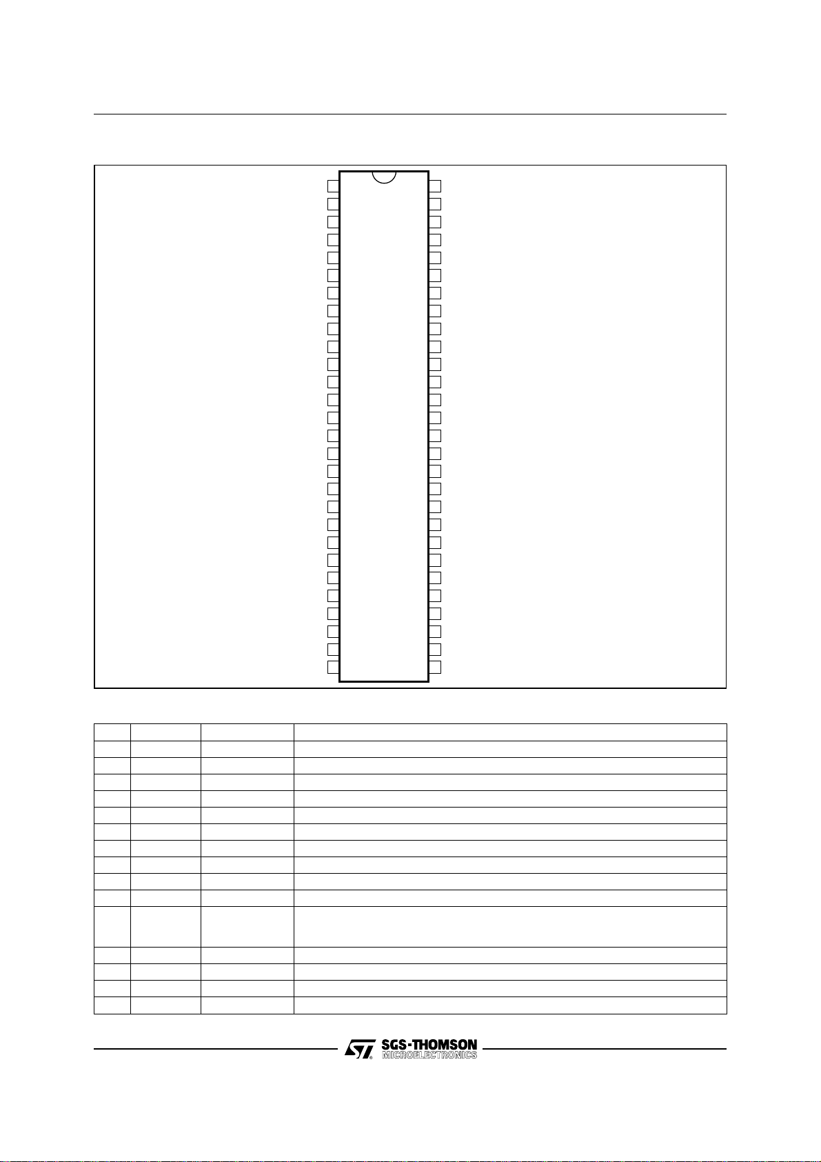
STV2162
PIN CONNECTIONS
WHITE STRETCH CAPACITOR
U INPUT
V INPUT
Y INPUT
APL CONTROL
VERTICAL SYNC INPUT
HORIZONTAL SYNC INPUT
27MHz CLOCK
NOT CONNECTED
GROUND
COLOR MATCHING
V
NOT CONNECTED
BLUE CUT-OFF REFERENCE
GREEN CUT-OFF REFERENCE
RED CUT-OFF REFERENCE
SOFSTART CAPACITOR
2
SERIAL CLOCK (I
SERIAL DATA (I
5V STANDBY (SHUNT REGULATOR)
ϕ
1 LOW PASS FILTER
LOOP
FOR SCANNING PART
V
CC
REFERENCE RESISTOR FOR CURRENT
REGULATOR OUTPUT
VERTICAL SAWTOOTH ERROR OUTPUT
RESISTOR BRIDGE POSITIVE INPUT
RESISTOR BRIDGE NEGATIVE INPUT
THT MODULATION AND PROTECTION
C BUS)
2
C BUS)
CC
GCUTREF
RCUTREF
WS
UIN
VIN
YIN
APL
VDFL
HDFL
LDFL
NC
GNDLIN
COLM
V
CCLIN
NC
BCUTREF
CSOFT
SCL
SDA
V5V
SLPF
V
I
REG
FROUT
SENSEP
SENSEM
BREATH
1
2
3
4
5
6
7
8
9
10
11
12
13
14
15
16
17
18
19
20
21
22
CC1
23
REF
24
25
26
27
28
56
YOUT
55
RES55
54
RES54
53
Y
52
NC
51
CONVAR
50
FBTXT
49
APX
48
BTXT
47
GTXT
46
RTXT
45
GNDVID
44
V
CCVID
43
ICUTOFF
42
ROUT
41
GOUT
40
BOUT
39
VABL
38
HDRIVE
37
SMPSOUT
36
TXT_OUT
35
SSC
34
GND1
33
HFLY
32
EWOUT
31
SMPSIN
30
EWIN
29
CVERT
Y OUTPUT OF WHITE STRETCH
RESERVED
RESERVED
Y INPUT VIDEO OF MAIN SIGNAL
NOT CONNECTED
CONTRAST VARIATION (FOR TRANSPARENT MENU)
FAST BLANKING INPUT FOR TEXT/OSD
AUTO PIX CAPACITOR
BLUE INPUT TEXT/OSD
GREEN INPUT TEXT/OSD
RED INPUT TEXT/OSD
GROUND FOR VIDEO PART
FOR VIDEO PART
V
CC
CUT-OFF AND LEAKAGE MEASUREMENT
RED OUTPUT
GREEN OUTPUT
BLUE OUTPUT
AVERAGE BEAM LIMITER INPUT
OUTPUT FOR HORIZONTAL DRIVER
PWM OUTPUT FOR SMPS
SYNC OUTPUT FOR TELETEXT/OSD
SSC SUPER SANDCASTLE OUTPUT
GROUND FOR SCANNING PART
HORIZONTAL FLYBACK INTERFACE
EAST/WEST OUTPUT
VOLTAGE INPUT FOR SMPS ERROR AMPLIFIER
EAST/WEST INPUT OF ERROR AMPLIFIER
VERTICAL AGC CAPACITOR
2162-01.EPS
PIN DESCRIPTION
Pin Name Function Description, Test Conditions, Remark
1 WS Time Constant White str etch time co nstan t adj ustmen t. Ext ernal capa citor , in terna l 20 0kΩ r esist or.
2 UIN Input B-Y signal, AC coupling
3 VIN Input R-Y signal, AC coupling
4 YIN Input Luminance before white stretch, AC coupling
5 APL Time Constant Auto Pedestal (APL) time constant. External capacitor, internal 200kΩ resistor
6 VDFL Input Vertical synchro
7 HDFL Input Horizontal synchro
8 LDFL Input 27MHz Line Clock
9 NC Reserved Not connected
10 GNDLIN Power supply Ground for Scanning Logic
11 COLM Control Color Matching strength. This pin must be grounded through a resistor .
12 V
CCLIN
Power supply VCC for Scanning Logic
13 NC - Not Connected
14 BCUTREF Reference Clamping B. Capacitor 47nF against Ground : cut-off Black Reference.
15 GCUTREF Reference Clamping G. Capacitor 47nF against Ground : cut-off Black Reference.
2/14
Resistor value determines Color Matching effect :
0 (short Circuit) = no effect, 44kΩ = maximal Colormatching.
2162-01.TBL
Page 3

STV2162
PIN DESCRIPTION
(continued)
Pin Name Function Description, Test Conditions, Remark
16 RCUTREF Reference Clamping R. Capacitor 47nF against Ground : cut-off Black Reference.
17 CSOFT Time Constant Capacitor for softstart, value determines softstart time (typ. 220µF).
2
18 SCL Input Serial Clock for I
19 SDA Input Serial Data for I
C bus
2
C bus (pull down - capability for acknowledge and data reply)
20 V5V Power supply Voltage supply for standby biasing, voltage is regulated via internal shunt
regulator
21 SLPF Time Constant Loop filter for horizontal VCO
22 V
23 I
CC1
REF
Power supply Supply voltage for Scanning part, connected with external series regulator
transistor.
Current
Reference
External programming resistor 1% metal type (25kΩ against V
the horizontal free running frequency.
). Determines
CC1
24 REG Output Output for controlling the external regulator transistor
25 FROUT Output Output of transconductance Frame Amplifier, pin has to be connected to the
inverting input of the vertical power amplifier.
26 SENSEP Input Input of internal resistor bridge for sensing the vertical deflection yoke current
27 SENSEM Input Input of Internal resistor bridge for sensing the vertical deflection yoke current
28 BREATH Input Two functions :
- if input voltage >1.5V, Vertical size (V_BREATING) and Horizontal width
(H_BREATING) compensation.
- if pin pulled down by external transistor : protection activated.
29 CVERT Reference Regulation of vertical sawtooth amplitude
30 EWIN Input Input of the error-amplifier for the East-West modulator
31 SMPSIN Input Input for the secondary Switch Mode Power Supply pulse width modulator
32 EWOUT Output Output of the error amplifier for the East-West modulator (current output, biasing
directly the darlington output transistor
33 HFLY Input Horizontal Flyback Input
34 GND1 Power supply Ground for all scanning functions
35 SSCOUT Output Super sandcastle output from the scanning processor part.
36 TXTOUT Output Composite 2H synchro for Teletext, OSD, ...
37 SMPSOUT Output Output for SMPS driver transistor
38 HDRIVE Output Open collector output for the horizontal line transistor
39 VABL Input Voltage input for the Average Beam Limiter function
40 BOUT Output Video output blue channel
41 GOUT Output Video output green channel
42 ROUT Output Video output red channel
43 ICUTOFF Input Input for the leakage and cut-off current measurement
44 V
CCVID
Power supply Voltage supply for the video part
45 GNDVID Power supply Ground for video
46 RTXT Input Input for red channel of TEXT/OSD
47 GTXT Input Input for green channel of TEXT/OSD
48 BTXT Input Input for blue channel of TEXT/OSD
49 APX Time constant External capacitor and resistor to determine the attack and delay time of th e APX
detector
50 FBTXT Input Fast Blanking input for TXT/OSD insertion (VFBTXT = 0 . . 3 V)
51 CONVAR Input Voltage at this Input d ecreases i nstantaneousl y the Contr ast : Contr ast-reducti on
for transparent Menu box
52 NC Reserved Not connected
53 Y Input Video input Y channel
54 RES54 Reserved Must be grounded
55 RES55 Reserved Must be grounded
56 YOUT Luma Output
Signal
Luminance output after white stretch.
(Application : connect YOUT with Y (Video Part) via capacitor of 47nF.)
2162-01.TBL
3/14
Page 4

4/14
RGB FBYINVINUIN
BLOCK DIAGRAM
STV2162
YIN
SDA
SCL
VDFL
HDFL
LDFL
SSC
WHITE STRETCH
LUMA
AVERAGE
DETECTOR
White Stretch
White Stretch
Control Function
I2C BUS AND
LATCHES
START-UP
LOGIC
Bus
2H-SANDCASTLE
GENERATOR
COLOR
EQUALIZER
ϕ
1 LOOP
TIME BASE
VOLTAGE AND
CURRENT
REFERENCE
RGB CLAMPING
AND DE-MATRIX
Bus
VIDEO
PROCESSOR
DEFLECTION PROCESSOR
Bus
HORIZONTAL
SWITCH
LOGIC
Video
Switch
PHI2 LOOP
FLYBACK
INTERFACE
AUTO
CONTRAST
CONTRAST
SATURATION
BRIGHTNESS
Bus
AVERAGE BEAM
CURRENT LIMITER
Bus
AUTO
PIEDESTAL
Bus
VERTICAL
PROTECTION
Bus
RGB
LOGIC
Bus
Bus
ROUT
GOUT
RGB
DRIVE
&
BOUT
ICUTOFF
VABL
CVERT
SENSM
SENSP
FROUT
BREATHING
EWIN
EWOUT
Bus
Bus
RGB
LIMITER
MEASUREMENT
SAWTOOTH
S-CORRECTION
BREATHING
EAST-WEST
CORRECTION
CUT-OFF
VERTICAL
VERTICAL
MATRIX
SMPSSOFT-START
STV2162
2162-02.EPS
VREF
IREF SYNCHRO
FOR
TXT OUT
HFLY
CSOFTHDRIVE
SMPS
SMPS
OUT
IN
Page 5
STV2162
ABSOLUTE MAXIMUM RATINGS
Symbol Parameter Value Unit
V5V Own Protection structure (Power-Zener-Protection-Diode) (Pin 20) 6 V
SCL,SDA Protection Structures connected to V5V (each of this pin has an
own Power-Zener-Protection Diode) (Pins 18-19)
VCCLIN,
Voltage regulated via ext.Transistor (Pins 12-22-44) 8.4V
VCCVID,
V
CC1
VSENSP,
Voltage on Pins 26-27 18 V
VSENSM
Toper Operating Ambient Temperature 0, 70
Tstg Storage Temperature -55 , +150
THERMAL DATA
Symbol Parameter Value Unit
R
th (j-a)
Junction-ambient Thermal Resistance Max. 40
7V
o
C/W
o
C
o
C
2162-02.TBL
2162-03.TBL
5/14
Page 6

STV2162
BUS DE SCRIPTION
1 - Slave-Address
Address : hex 8C/8D
MSB LSB
1000110Read-Write
2 - Address-Mapping
(write mode)
x = don’t care-bits, not used in the decoding of the subaddress.
Subaddress Data Bits
(binary) dec hex MSB LSB
xxx00000 0 00 VID_ACT S_ON H_VCO
xxx00001 1 01 S_CORR_3 S_CORR_2 S_VOLTAGE
xxx00010 2 02 S_CORR_1 S_CORR_0 EW_SHAPE
xxx00011 3 03 MPX_3 MPX_2 EW_AMPLITUDE
xxx00100 4 04 MPX_1 MPX_0 HPOS_5 HPOS_4 HPOS_3 HPOS_2 HPOS_1 HPOS_0
xxx00101 5 05 FSCK EW_TILT
xxx00110 6 06 AUTO_VCR FORCE_VCR H_WIDTH
xxx00111 7 07 TST_V1 TST_V0 V_DC
xxx01000 8 08 V_AMPLITUDE
xxx01001 9 09 VPAN_2 H_RIGHT_BLANKING
xxx01010 10 0A VPAN_1 VPAN_0 H_LEFT_BLANKING
xxx01011 11 0B APL_LEVEL
xxx01100 12 0C H_BREATHING V_BREATHING
xxx01101 13 0D VSTART_4 VSTART_3 VSTART_2 CEQU_4 CEQU_3 CEQU_2 CEQU_1 CEQU_0
xxx01110 14 0E VSTART_1 VSTART_0 WS_THRESHOLD
xxx01111 15 0F NTSC_PAL WS_ON CONTRAST
xxx10000 16 10 EWS12 ENVPS BRIGHTNESS
xxx10001 17 11 STOP_C_VAR DRV_GAIN SATURATION
xxx10010 18 12 RGB_LIM APX_THRESHOLD
xxx10011 19 13 V_CORR_3 V_CORR_2 R_CUTOFF
xxx10100 20 14 V_CORR_1 V_CORR_0 G_CUTOFF
xxx10101 21 15 RES_CUT FUF R_DRIVE
xxx10110 22 16 VID_OFF DIS_CUT G_DRIVE
xxx10111 23 17 SSC_TRI FORCE_ MUTE B_DRIVE
Subaddress 0
MSB LSB
X XVID_ACTS_ONH3H2H1H0
(hex 00)
VID_ACT : Video Processor Activation
Switch to activate Video processor
0 : Startup phas e : Video outpu t (R,G,B_ OUT) hard bl anked (0.9V) , no cu t-off ins ertion lines
1 : RGB outputs active
S_ON : TV Mode Selection
Switch to change from standby mode to operation mode
0 : Stan dby o pera tion : I
1 : TV set = ON : V
2
C bus active ; Protection logic active ; Pin REG pulled down to ground
regulator active
CC
H[3..0] : Hor izontal Free Running Frequency
H_VCO 0000 (hex 0) minimal free running frequency
1111 (hex F) maximum free running frequency
6/14
Page 7

STV2162
BUS DE SCRIPTION
Subaddress 1
(continued)
(hex 01)
& System-V oltage -
MSB LSB
S_CORR_3 S_CORR_2 S5 S4 S3 S2 S1 S0
S_CORR_3,
: S _Correction (2 MSB) (see subaddress 2)
S_CORR_2
S[5..0] : System Voltage Adjustment (S_VOLTA GE )
S_VOLTAGE 000000 (hex 00) minimal position : System voltage minimal
111111 (hex 3F ) maximal position : System voltage maximal
Subaddress 2
MSB LSB
S_CORR_1 E5 E4 E3 E2 E1 E0
S_CORR_1,
S_CORR_0
(hex 02)
: S _Correction (2 LSB)
S_CORRECTION 0000 (hex 0) minimal S_Correction (vertical sawtooth flat)
1111 (h ex F) maximal S_Correction
E[5..0] : EW_Shape (corner correction)
EW_SHAPE 000000 (hex 0) mini mal parabola flattening (ideal parabola)
111111 (hex 3F) maximal parabola flattening (flattened corners of parabola)
Subaddress 3
MSB LSB
0 0 E5 E4 E3 E2 E1 E0
(hex 03)
E[5..0] : EW -A mplitude
EW_AMPLITUDE 000000 (hex 00) minimal Parabola-Amplitude = 0V (=no Parabola)
111111 (hex 3F) maximal Parabola-Amplitude = 0.7V
Subaddress 4
MSB LSB
0 0 H5 H4 H3 H2 H1 H0
(hex 04)
H[5..0] : Horizontal Picture Position (left-right -shift)
H_POSITION : fine tuning of reference slope
H_POSITION 000000 (hex 00) minimal position :
rising edge of HDFL in the middle of HFLY.
100000 (hex 20) nominal position
1 11111 (hex 3F) maximal position :
rising edge of HDFL 4.7µs before middle of HFLY.
7/14
Page 8

STV2162
BUS DE SCRIPTION
Subaddress 5
(continued)
(hex 05)
East-West - Tilt (Unsymmetry):
MSB LSB
FSCK E5 E4 E3 E2 E1 E0
FSCK : Selector for free run horizontal frequency (start) of 27MHz clock operation
0 : Normal operation = external 27MHz Clock (LDFL) used to control horizontal deflection after
the softstart operation and video identification (VIDID=1)
1 : Internal clock
E[5..0] : East/W est T ilt (unsymm etry)
EW_TILT 000000 (hex 00) minimal position :
parabola unsymmetrical, (higher on the top of the picture)
100000 (hex 20) nominal position : parabola symmetrical
111111 (hex 3F) maximal position :
parabola unsymmetrical, (lower on the top of the picture)
Subaddress 6
MSB LSB
AUTO_VCR FORCE_VCR H5 H4 H3 H2 H1 H0
(hex 06)
AUTO_VCR / FORCE_VCR : VCR Mode Selection
TV-Mode FORCE_VCR AUTO_VCR
PHI1 loop forced to NOVCR mode (TV operation) 0 0
VCR trick mode automatically detected and VCR mode forced (Trick mode = not 312.5
lines per frame in 100Hz mode ; not 265.5 lines per frame in 120Hz mode )
Phi1 loop forced to VCR mode 1 0
Test mode for vertical countdown logic test ( only IC testing) 1 1
01
H[5..0] : H_WIDTH (p icture width controlled by the East/West modulator)
H_WIDTH 000000 (hex 00) minimal picture size
111111 (hex 3F) maximal picture size
Subaddress 7
MSB LSB
0 0 V5 V4 V3 V2 V1 V0
(hex 07)
V[5..0] : Vertical Position (vertical DC shift)
V_DC 000000 (hex 00) picture s hi f ted down
1 11111 (hex 3F) picture shifted up
Subaddress 8
MSB LSB
X V6V5V4V3V2V1V0
(hex 08)
V[6..0] : Vertical S awtooth Amplitude
V_AMPLITUDE 0000000 (hex 00) minimal amplitude
(0.65V
(between270 lines) on SENSP/SENSM)*
PP
1111111 (hex 7F) maximal amplitude
(1.73V
(between270 lines) on SENSP/SENSM)*
PP
* : With no vertical power safe function.
8/14
Page 9

STV2162
BUS DE SCRIPTION
Subaddress 9
MSB LSB
(continued)
(hex 09)
VPAN_2 X H4 H3 H2 H1 H0
VPAN_2 : Vertical Panning (1 MSB) (see subaddress 10)
H[4..0] : Horizontal Blanking on right picture side (reference slope : middle of HFLY)
H_RIGHT_BLANKING 00000 (hex 0) minimal horizontal oversize blanking (-2µs)
11111 (hex 1F ) maximum hori zo ntal oversize blanking
(-6.74µs on right side)
Stepsize ~ 0.15µs
Subaddress 10
MSB LSB
VPAN_1 X H4 H3 H2 H1 H0
VPAN_1,
VPAN_0
(hex 0A)
: Vertical Panning (2 LSB)
VPAN 000 (hex 0) no vertical panning (no vertical deflection delay)
111 (hex 7) maximum vertical panning = 30 lines delay of vertical deflection
Stepsize : 4 lines delay
H[4..0] : Horizontal Blanking on left picture side
H_LEFT_BLANKING 00000 (hex 00) minimal horizontal oversize blanking (+2µs)
11111 (hex 1F ) maximum hori zo ntal oversize blanking
(+6.74µs on left side)
Stepsize ~ 0.15µs
Subaddress 1 1
MSB LSB
A3 A2 A1 A0 V3 V2 V1 V0
(hex 0B)
A[3..0] : Auto Pedestal Level "APL_LEVEL" ( adaptive brightness)
APL_LEVEL 0000 (hex 0) minimal value = no influence = 0 IRE
1 111 (hex F) maximal value = maximum brightness increase
(20 IRE when luma averagevalue 100 IRE)
V[3..0] : Vertical Blanking (also changes vertical fix points for S_Correction and East/West parabola)
V_BLANKING 0000 (hex 00) minimal value of fix points and vertical blanking
(0.52V on SE N SM /S ENSP)
1 111 (hex 0F) maximal value of fix points and vertical blanking
(0.6V on SE NSM/SENSP)
Subaddress 12
MSB LSB
H3 H2 H1 H0 V3 V2 V1 V0
(hex 0C)
H[3..0] : Horizontal Breathing
H_BREATHING 0000 (hex 0) minimal Horizontal Breathing (0%)
1111 (hex F) maximal Horizontal Breathing (10%)
V[3..0] : Vertical Breathing
V_BREATHING 0000 (hex 0) minimal Vertical Breathing (0%)
111 1 (hex F) maximal Vertical Breathing (10%)
9/14
Page 10

STV2162
BUS DE SCRIPTION
Subaddress 13
MSB LSB
VSTART_4 VSTART_3 VSTART_2 C4 C3 C2 C1 C0
VSTART_4,
: Vertical Ramp Start Panning (3MSB) (see subaddress 14)
(continued)
(hex 0D)
VSTART_3,
VSTART_2
C[4..0] : Color Equalizer (differential gain between UIN- and VIN- channel)
COLOR_EQUALIZER 00000 (hex 00) minimal position :
max. gain for UIN, min. gain for VIN
10000 (hex 10) nominal position : same gain for UIN and VIN
11111 (h ex 1F) maximal position :
min. gain for UIN, max. gain for VIN
Subaddress 14
MSB LSB
VSTART_1 VSTART_0 W5 W4 W3 W2 W1 W0
VSTART_1,
VSTART_0
(hex 0E)
: Vertical Ramp Start (2 LSB)
VSTA RT 00000 (hex 0) vertical ramp start at line 0
11111 (hex 1F) vertical ramp start at line 64
W[5..0] : White Stretch Threshold
WS_THRESHOLD 000000 (hex 00) minimal position : threshold value = 5 IRE
111111 (hex 3F) maximal position : threshold value = 40 IRE
Subaddress 15
MSB LSB
NTSC_PAL WS_ON C5 C4 C3 C2 C1 C0
(hex 0F)
NTSC_PAL : RGB Matrix Selection
0 : RGB matrix uses the PAL/SECAM - Coefficients for the Conversion YUV -> RGB
1 : RGB matrix uses the NTSC - Coefficients for the Conversion YUV -> RGB
Note :
The input-dematrix for RGBTXT is always "PAL/SECAM" dematrix !! i.e. at the NTSC-mode the colors are correct only for YUV-input.
WS_ON : White Stretch Selection
0 : White Stretch is switched off
1 : White Stretch is actived
C[5..0] : Contrast Adjustment
CONTRAST 000000 (hex 00) minimal position : smalles contrast level
= 20% of maximal contrast
111111 (he x 3F) maximal position : maximal contrast
Subaddress 16
MSB LSB
EWS12 ENVPS B5 B4 B3 B2 B1 B0
(hex 10)
EWS12 : Selection of Parabole Corner Type
ENVPS : Vertical Power Safe Selection
0 : v ertical power safe function not active
1 : v ertical power safe function active
B[5..0] : Brightness
BRIGHTNESS 000000 (hex 00) minimal position : brightness = -30 IRE
100000 (hex 20) nominal position : brightness = 0
111111 (hex 3F) maximal position : brightness = +30 IRE
10/14
Page 11

STV2162
BUS DE SCRIPTION
Subaddress 17
MSB LSB
STOP_C_VAR DRV_GAIN S5 S4 S3 S2 S1 S0
(continued)
(hex 11)
STOP_C_VAR : Contrast V ariation with TXT insertion
with this bit, the user saturation and contrast setting will be partially removed i.e. moved
toward contrast = max., saturation = 100% (middle) for TXT/OSD insertion (RTXT,
GTXT, BTXT))
0 : TXT/OSD insertion : same contrast as main channel
1 : TXT/OSD insertion (FBTXT=1) toward max. contrast and mid. saturation
DRV_GAIN : Selection of gain range (changes the range of the gain adjustement drive)
0 : maximum gain = 4.6
1 : maximum gain = 6.5
S[5..0] : Color Saturation Adjustment
SATURATION 000000 (hex 00) minimal position = completely suppressed colors
111111 (hex 3F) maximal positio n : maximal saturation ( 3dB
oversaturation)
Subaddress 18
MSB LSB
RGBLIM1 RGBLIM0 A5 A4 A3 A2 A1 A0
(hex 12)
RGBLIM[1..0] : RGB Hard Limiter
Voltage limitation of R,G,B at the output of the matrix , just before drive adjustment
RGB_LIM 00 (hex 0) limitation at 100 IRE
1 1 (hex 3) limitation at 150IRE
A[5..0] : Auto Pix (APX) Threshold Voltage
APX_THRESHOLD 000000 (hex 00) minimal position : threshold value = 50 IRE
111111 (hex 3F) maximal position : threshold value = 100 IRE
Subaddress 19
MSB LSB
V_CORR_3 V_CORR_2 R5 R4 R3 R2 R1 R0
V_CORR_3,
(hex 13)
: Vertical Corner Point of EW Shape (2 MSB) (see subaddress 20)
V_CORR_2
R[5..0] : Red Cut-off Adjustment (Blue is fixed value of 0.45V at BOUT)
R_CUTOFF 000000 (hex 00) insertion of 0.675V at ROUT for red measurement pulse
111111 (hex 3F) insertion of 0.225V at ROUT for red measurement pulse
Subaddress 20
MSB LSB
V_CORR_1 V_CORR_0 G5 G4 G3 G2 G1 G0
V_CORR_1,
V_CORR_0
(hex 14)
: Cor ner Point of EW-Shape (2 LSB)
V_CORNER 0000 (hex 0) corner point of EW shape @ 60% of fix point
1111 (h ex F) corner point of EW shape @ 80% of fix point
G[5..0] : Green Cut-off Adjustment (Blue is fixed value of 0.45V at BOUT)
G_CUTOFF 000000 (hex 00) insertion of 0.675V at GOU T for green measurem ent pulse
111111 (hex 3F) insertion of 0.225V at GOUT for green measurement pulse
11/14
Page 12

STV2162
BUS DE SCRIPTION
Subaddress 21
MSB LSB
RES_CUT FUF D5 D4 D 3 D2 D1 D0
(continued)
(hex 15)
RES_CUT : Reset of Cut-off Counters and TUBE_COLD bit ; at the same time : stop of cut-off function
0 : c ut-off loop active
1 : cut-off loop stopped and Reset of all cut-off counters and TUBE_COLD bit
FUF : Full Frame Mode (selects cut-off loop operation modus)
0 : c ut-off loop is active during the whole frame (adjustment of VG2 on the CRT board in
production)
1 : c ut-off loop is active during the first 4 active Video lines : normal mode
D[5..0] : Drive Register for Red Channel (gain adjustement of the red driver output stage)
R_DRIVE 000000 hex 00) minimal position : 0.33 of maximal value
111111 (hex 3F ) maximal position : 3.2VPP at ROUT for contrast = max.,
DRV_G AIN=1 and Y= 70 IRE; or DRV _GAIN=0 and Y = 100 IRE
Subaddress 22
MSB LSB
VID_OFF DIS_CUT D5 D4 D3 D2 D1 D0
(hex 16)
VID_OFF : Hard Blanking of Video Output
0 : normal operation
1 : ROUT, GOUT, BOUT is hard blanked, while the cut-off measurement is still active.
DIS_CUT : Disable of Cut-off Loop
0 : Cut-off loop is active.
1 : Cut-off loop is stopped, actual values in the registers are frozen.
Truth - Table for DIS_CUT / FUF
Operation Mode DIS_CUT FUF
Video signal present at RGBOUT ; 3 cut-off measurement lines in the lines 21,22,23 0 0
Cut-off measurement during the whole frame with the sequence --> Leakage - Blue, green, red
(repetitive each 4th line)
Video signal pre sent at RGBOUT but no cut-off measurement (last values of cut-off cou nter frozen) 1 0
All Outputs ROUT, GOUT, BOUT hard blanked all the time ; no video ; no cut-off measurement
(useful when TV is switched off --> immediate stop of video output)
01
11
D[5..0] : Green Drive Register (gain adjustement of the GREEN driver outputstage)
G_DRIVE 000000 (hex 00) minimal position : 0.33 of maximal value
111111 (hex 3F ) maximal position : 3.2 V
at GOUT for contrast = max.,
PP
DRV_GAIN=1 and Y=70 IRE ; or DRV_GAIN=0 and Y=100 IRE
Subaddress 23
MSB LSB
SSC_TRI FORCE_MUTE D5 D4 D3 D2 D1 D0
(hex 17)
SSC_TRI : Mode switch for super sandcastle output (only useful in test mode)
0 : SSC Pin delivers super sandcastle output
1 : Super sandcastle output disabled ; Pin SSC can serve as input for PSI and video part
FORCE_MUTE : Test mode for accelerating the test of the PHI1 mute circuit
0 : normal operation ; TV application
1 : PHI1 circuit set to mute ; ϕ1 forced to free run mode
D[5..0] : Blue Drive Register (gain adjustement of the blue driver output stage)
B_DRIVE 000000 (hex 00) minimal position : 0.33 of maximal value
111111 (hex 3F ) maximal position :
3.2 V
at BOUT for c ontrast = max., DRV_GA IN=1 and
PP
Y=70 IRE ; or DRV_GAIN=0 and Y=100 IRE
12/14
Page 13

STV2162
BUS DE SCRIPTION
3 - Output Signals
Reply
Byte
1st PONRESET OVERLOAD VIDID S120/100 VSTD TUBECOLD PHI1MUTE SYNCVID
2nd LSB_R_CUT LSB_G_CUT LSB_B_CUT VERS _NBR VERS _EXT
3rd R_CUTOFF_COUNTER
4th G_CUTOFF_COUNTER
5th B_CUTOFF_COUNTER
MSB LSB
(continued)
(Read-Mode)
PONRESET : 1 if voltage drop on V5V (< 4.5V) has been detected (risk of data loss in latch
memory)
OVERLOAD : 1 if after 3 restart trials TV set is switched off definitely since breathing pin was
pulled down due to an error (reset to 0 can be done by switching off the TV
set (S_ON = 0 ; see Subaddress 0)
VIDID : 1 if Start-Oscillator PHI1 islocked to HDFL pulse after 7 francs
0 if not
S120/100 : 1 if vertical sync pulse frequency = 120Hz
0 if vertical sync pulse frequency = 100Hz
VSTD : 1 if line-numbers per frame are interlace standard : exactely 312.5 (100Hz) or
262.5 (120Hz)
0 if line-numbers per frame are different from this standard -> VCR trick mode
recognition
TUBECOLD : 1 after start of TV set
0 if the first time one of the cut-off counters is decremented ( tube starts to
deliver beam current)
PHI1MUTE : 1 if PHI1 loop is in mute mode ( no valid HDFL detected ) ; SLPF connected
to a fix voltage
SYNCVID : 1 if Start oscillator PHI1 is in phase to HDFL pulse
0 if not
VERS_NBR : Version number
VERS_EXT : Version extention
LSB_R_CUT : LSB of 9 bit red cut-off counter
LSB_G_CUT : LSB of 9 bit green cut-off counter
LSB_B_CUT : LSB of 9 bit blue cut-off counter
R_CUTOFF_COUNTER : Returns the 8 MSB of the 9 bitred cut-off counter
G_CUTOFF_COUNTER : Returns the 8 MSB of the 9 bit green cut-off counter
B_CUTOFF_COUNTER : Returns the 8 MSB of the 9 bit blue cut-off counter
13/14
Page 14

STV2162
PACKAGE MECHANICAL DATA
56 PINS - PLASTIC SHRINK DIP
Dimensions
Min. Typ. Max. Min. Typ. Max.
Millimeters Inches
A 5.08 0.200
A1 0.51 0.020
B 0.35 0.59 0.014 0.023
B1 0.75 1.42 0.030 0.056
C 0.20 0.36 0.008 0.014
D 52.12 2.052
D1––––––
E 18.54 0.730
E1 13.72 0.540
K1––––––
K2––––––
L 2.54 3.81 .100 0.150
e1 1.78 0.070
Number of Pins
N56
Information furnished is believed to be accurate and reliable. However, SGS-THOMSON Microelectronics assumes no responsibility
for the consequences of use of such information nor for any infringement of patents or other rights of third parties which may result
from its use. No licenc e is gra nted by impl ication or ot herwise under any patent or pat ent ri ghts of SGS-THOMSON Microelectronics.
Specifications mentioned in this publication are subject to change without notice. This publication supersedes and replaces all
information previously s upplied. SGS -THOMSON Mic roelectroni cs products are not authorize d for use as critical compone nts in life
support devices or systems without express written approval of SGS-THOMSON Microelectronics.
PMSDIP56.EPS
SDIP56.TBL
14/14
1997 SGS-THOMSON Microelectronics - All Rights Reserved
©
2
Purchase of I
2
C Patent. Rights to use these components in a I2C system, is granted provided that the system conforms to
I
Australia - Brazil - Canada - China - France - Germany - Hong Kong - Italy - Japan - Korea - Malaysia - Malta - Morocco
The Netherlands - Singapore - Spain - Sweden - Switzerland - Taiwan - Thailand - United Kingdom - U.S.A.
C Components of SGS-THOMSON Microelectronics, conveys a license under the Philips
2
C Standard Specifications as defined by Phili ps.
the I
SGS-THOMSON Microelectronics GROUP OF COMPANIES
 Loading...