

Page 1
BUS CONTROLLED PAL/SECAM/NTSC TV PROCESSOR
.
I2C BUS CONTROL OF ALL FUNCTIONS
.
INTEGRATED FILTERS
(TRAP,BANDPASS, CLOCHE)
.
INTEGRATED LUMINANCEDELAYLINE
.
PAL/SECAM/NTSCCHROMADEMODULATORS
.
AUTOMATIC CUT-OFF CURRENTLOOP
.
TWORGB INPUTS
.
SVHSSWITCH
.
TWOPLLs HORIZONTALDEFLECTION
.
VERTICALCOUNT DOWN
.
VERYFEW EXTERNALCOMPONENTS
DESCRIPTION
The STV2118Bis a fully bus controlled IC for TV
luma, chroma and deflectionprocessing.
Used withSTV8224 (PIF/SIF/switches), TDA1771
or TDA8174(framebooster),STV2180(delayline),
it allows to design a PAL/SECAM/NTSC
(BGDKILMN) set with very few external components and no adjustment.
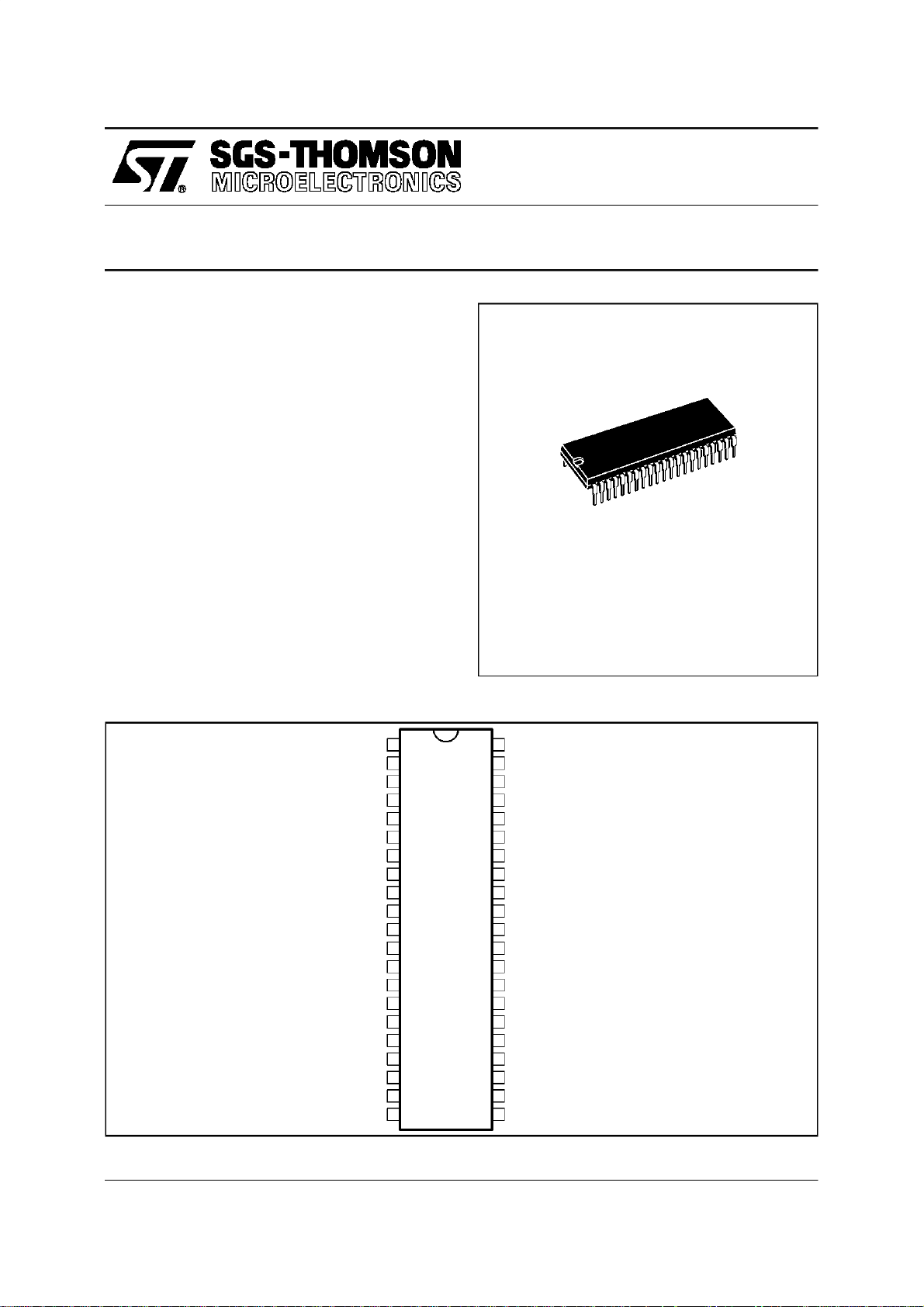
STV2118B
SHRINK42
(Plastic Package)
ORDER CODE : STV2118B
PINCONNECTIONS
CHROMA/SCANNING GROUND
ACC CONTROLCAPACITOR
CLOCHE FILTER TUNING
VOLUME ANDMUTE CONTROL VOLTAGE
IF STANDARD AND SWITCH S ELECTION
EXTERNAL BLUE INPUT
EXTERNAL GREEN INPUT
EXTERNAL RGB INSERTION
CVBS OR LUMINANCE INPUT
3.58MHz XTAL
4.43MHz XTAL
CHROMA LOOP FILTER
DATAWIRE I
CLOCK WIRE I
OSD GREEN INPUT
OS D RGB INSERTION
EXTERNAL RED INPUT
2
C BUS
2
C BUS
FILTER TUNING
OS D BLUE INPUT
OS D RED INPUT
ACC
SDA
SCL
VOL
SWI
1
2
3
4
5
6
7
8
9
10
11
12
13
14
15
16
17
18
19
20
21 22
GND2 V
CXTL2
CXTL1
CLPF
FTUN1
FTUN2
BOSD
GOSD
ROSD
FBOSD
BEXT
GEXT
REXT
FBEXT
Y/CVBS
GND1
42
41
40
39
38
37
36
35
34
33
32
31
30
29
28
27
26
25
24
23
CC2
BYO
RYO
RYI
BYI
LFB/SC
HOUT
VOUT
VAMP
SLPF
SXTL
BCL
ICAT
RO
GO
BO
CR
CB
CG
CHR/SVHS
V
CC1
CHROMA/SCANNING/BUS SUP P LY
B-Y OUTPUT
R-Y OUTPUT
R-Y INPUT
B-Y INPUT
LINE FLYBACK INPUT/SANDCASTLE OUTPUT
HORIZONTAL OUTP UT
VERTICAL OUTPUT
AMPLITUDE CONTROL VOLTAGE
SCANNING LOOP FILTER
503kHz CERAMIC
BEAM CURRENT LIMITER
CATHODE CURRENT MEASUREMENT
RED OUTPUT
GREEN OUTPUT
BLUE OUTPUT
RED CUT-OFF CAPACITOR
BLUE CUT-OFF CAPACITOR
GREEN CUT-OFF CAPACITOR
CHROMINANCE INPUT/SVHS SELECTION
VIDEO SUP PLYBUS/VIDEO GROUND
2118B-01.EPS
June 1996
1/25
Page 2
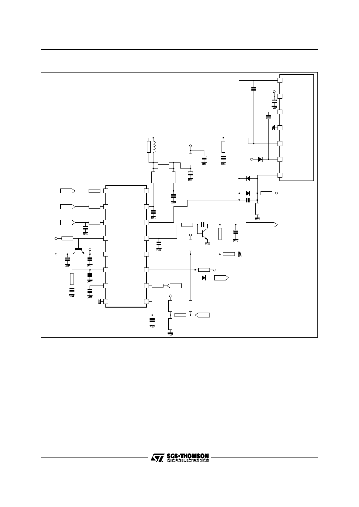
STV2118B
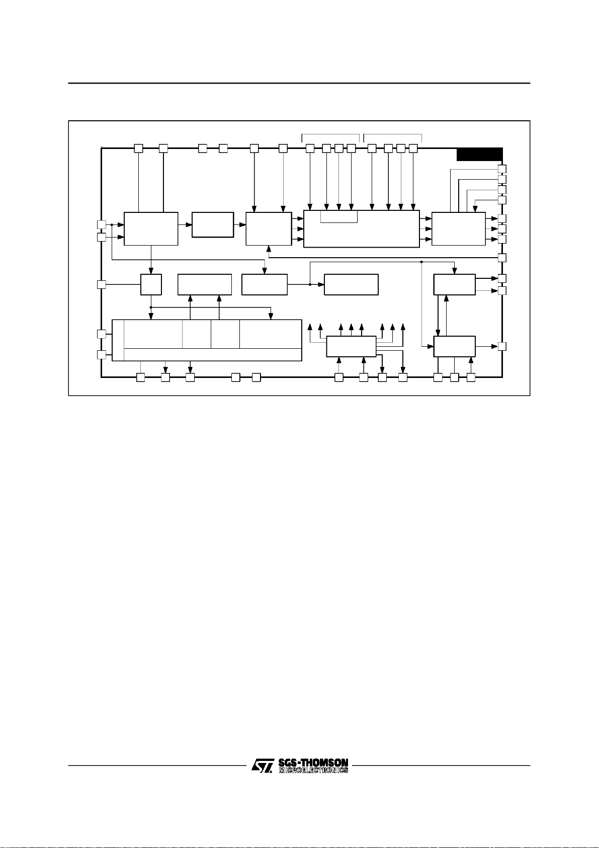
BLOCK DIAGRAM
FILTER
TUNING
89
2
3
FILTER TUNING
TRAP BANDP ASS
CLOCHE
SVHS SWITCH
CHR
ACC5
SECAM
DEMODULATOR S
PLL
Y/CVBS
CHR
ACC
CXTAL2
CXTAL1
20
23
CLOCHE
TUNING
Y
IDENTIFICATION
DELAYLINE INTERFACE
V
V
CC1
22 42 19 18 17 1639 38
DELAY
LINE
SHARP NESS
STANDARD
SECAM
KILLER
NTSC
KILLER
CC2
PAL/
R-Y B-Y
SATURATION
BRIGHTNE SS
SEPARATOR
DEMODULATOR S
MATRIX
CONTRAST
SYNC
PAL/NTSC
EXTERNAL OS D
FB RGBFBRG B
Contras t
IDENTIFICATION
SHARP
HUE
DECODER
15 14 13 12
RGB SWITCHES
VIDEO
BRIG
SAT
CONT
BUS
STD
DRIVE
CUT-OFF
STV2118B
BLANKING
AUTO CUT-OFF
BLACK&WHITE
CONTRO L
FRAME
SCANNING
LINE
SCANNING
25
CB
CG
24
26
CR
30
ICAT
29
R
28
G
27
B
BCL
31
VOUT
35
34
VAMP
36
HOUT
44041
21 1 373332
GND2 SWI VOLCLPF R-Y B-Y
GND1
6 7 11 10
SDA SCL
SXTAL SLPF
LFB/SC
2118B-02.EPS
2/25
Page 3

FUNCTIONAL DESCRIPTION
1 - DEFLECTION CIRCUIT
Note : [X,Y] : line number referred to the internal
line counternumbering
- Fullyintegratedsynch. separator,withalowpass
filter, a blacklevelalignmentof the Y/CVBSinput,
a slicing level at 2/3,1/3 of the sync. pulseamplitude.
- Frame sync. pulse locked on 2 f
frequency to
H
perfect interlace.
- 500kHzVCOwithan externalceramicresonator.
- Twophase locked loops
• thefirst PLLlocksthe VCO on thevideo signal
frequency,
• thesecondPLLcompensatestheline transistor
storage time.
- Three time constants for the first PLL.
• thelong timeconstantisused for normal opera-
tion
• the short time constant is automatically used
during the frameretraceand in searchmode of
VCR when theframe pulse is outside[258,264]
and [309,314].
• verylongtimeconstantwhenno video recogni-
tion
Timeconstants in normaloperation
(automatic selection of time constants) :
50Hzinput signal :
- short time constant : [306, 21]
- longtime constant : the restof the field
60Hzinput signal :
- short time constant : [0, 16]
- longtime constant : the restof the field
• inhibitionof the first PLL :
the first locked loop is opened from line 309 to
line 4.5(or314)in50Hzmode.It is openedfrom
line 258 to line 5.5 (or 264) in 60Hz mode.
• thetime constantsvaluesare chosenbymeans
of external components.
• possibility to force the short time constant
through the bus.
• possibility to force the very long time constant
through the bus.
- Video identification : coincidence detector between the line synchro top and a line frequency
windowfromthefirst PLL.Thevideoidentification
statusisavailableinthe outputregisterof the I
2
C
bus decoder.
- Generation of burst gate pulses and line frequency signals from the first PLL to drive the
STV2118B
chroma and video circuits. The burst gate pulse
is alsosent to the sandcastlegenerator.
- Framesynchrowindow :
[248, 352] catching
- Field frequency selectionwindows :
[248, 288] 60Hz mode selection if two
consecutive frame pulses occur
insidethiswindow,otherwise50Hz
mode selection.
[288, 352] 50Hz mode selection window
- frameblanking pulse :
from line 0 to 21 in50Hzmode
from line 0 to 16 in60Hzmode
- Verticaloutput pulse is 10.5 lineslong.
- Horizontal output pulse : 28µs line pulse on an
open collectoroutput;
- Start up circuit: the horizontaloutput is at a high
level when V
shutting down, horizontal pulses are disabled
when V
CC
- Soft-startcircuit : the duty cycleof the horizontal
output is78 %(Thigh/(Thigh+TLow))whenV
is lower than (0.75 x V
time.
During the falling time, a 78% duty cycle HOUT
pulse is provided when V
(0.60 x V
CC2
- Possibilityto disable the horizontal output pulse
through the bus (forcea high level onHOUT).
- Horizontalposition adjustmentcontrolled by bus.
- Buscontrolledoutputvoltagetoadjustthevertical
amplitude;this voltagepermitsto adjusttheslope
of the verticalsawtoothgeneratedbythe external
frame booster.
- Buscontrolledvertical position; thehigh levelof
the vertical pulse permits to adjust the vertical
position.
- Bus controlled 4/3-16/9 selection : the low level
of theverticalpulseis0.1Vwhen16/9isselected,
2V when4/3 is selected.
- Combined flyback input and sandcastle output
(Pin 37).
Two thresholds on LFB/SCO Pin : The lowest
threshold(0.7V) permits to extractthelineblanking pulse; the highest threshold (2V) permits to
extract the line pulse for PLL2.
The sandcastlesignalat Pin 37is usedto control
the externalbaseband chromadelay line.
increases from 0 to 6.8V. On
CC
isbelow 6.2V.
), during the rising
CC2
CC1
).
CC1
is lower than
3/25
Page 4

STV2118B
FUNCTIONAL DESCRIPTION (continued)
2 - FILTERS
- Integrated trap filter :
f
−3dB
1
f
f
o
−3dB
−
f
o
Q =
Centerfrequency : - 4.43MHz,
- 4.25MHz, for SECAM
- Integratedchromabandpass :
Q = 3.5
Centerfrequency: 4.43MHz, 3.58MHz
- Integratedcloche filter for SECAM:
Q=16
Centerfrequency: 4.286MHz
- Integrateddelay line :
Bandwidth = 8MHz
- Integratedlow passfilter fordeflection part.
- All filtersare tunedwith a referencephaselocked
loop.
The PLL consists of a lowpass filter, a phase
comparator,a loop filter (an external capacitor).
The reference signal is the continuous carrier
wave from the VCO (4.43MHz or 3.58MHz). The
PLLadjusts the center frequency of the lowpass
so that it is equal to the reference signal. The
tuningvoltageof thePLLisusedtoadjustallother
filters.Theclochefilteris finetuned witha second
PLLoperating during frame retrace.
3 - VIDEO CIRCUIT
- 2 RGB inputs : RGB (OSD) input has priority
againstthe RGBext. Maximum contraston RGB
(OSD).-12dB range contrast control on RGBext.
Q = 1.7 at sharp.min
Q = 3.0 at sharp. max
3.58MHzfor PAL, NTSC
(f
= 3MHz ; -20dB
-3dB
rejection between 4.1MHz
and 4.4MHz)
Possib ility to disable the RGBext insertio n
through the bus.
- Oversizeblanking capabilityon FB(OSD)(Pin15)
input. The RGB ouputs will be blankedwhen the
voltageon Pin15 willexceedthe secondthreshold at 1.9V (blanking threshold) : the whole field
is blankedbutnotthe insertedcut-off pulses.The
OSDinsertion thresholdis 0.7V.
- Automaticcut-off current loop : 2V cut-off range.
Sequential cut-off current measurement during
the three lines after the frame blanking signal.
Leakage current measurementduring the frame
blanking,memorizationon an internal capacitor.
- Possibility to force through the bus the inserted
cut-off pulses on lines 23/24/25(CCIR) in 50Hz
and 60Hzmode.
- Warmup detector.
- Beamcurrent limiter DC voltageinput.
The beam current limiter control voltage will act
on contrast first, then the brightness will be decreasedwhen contrastattenuationreaches-5dB.
- Bus control of the red, green and blue channel
gain (White pointadjustment)
- Buscontrolofthe red andgreen DC levels (black
point adjustment)
- PAL and SECAM matrix, specific NTSC matrix
when demodulationangles are (0
o
,104o).
- Switch-offof the trap filterin SVHSmode.
- Buscontrolledcontraston luminance
(20dBrange)
- Buscontrolledsaturation (50dB range)
- Bus controlled brightness : 40% range at maximum contrast.
- Bus controlled sharpness (peaking); sharpness
active in PAL/NTSC standardonly.
- Noisecoring function on sharpness.
4/25
Page 5

FUNCTIONAL DESCRIPTION (continued)
4 - CHROMACIRCUIT
4.1 - PAL/SECAM/NTSC Decoders
- SVHS inputs ; bus controlledSVHS mode.
- 30dB range ACC
- Use of an exter nal base ba nd d elay l ine
(STV2180recommended)
- Automaticstandardidentification,with possibility
to force the standard throughthe bus.
4.2 - PAL/NTSC Decoders
- ACC doneby peakdetector on synchronousdemodulationof the burst
- Fullyintegrated killer functions.
- VCO using two standard crystals: 4.43MHzand
3.58MHz. One crystal is internally selected dependingon the standard selection.
XTALSPECIFICATION:
Frequency:
4.433619MHz(PAL/SECAM)
3.579545MHz(NTSC M)
3.575611MHz(PAL M)
3.582056MHz(PALN)
Vibrationmode : Fondamental,seriesresonance
(no serial capacitor)
Motionalcapacity : 13fF ±3fF
Resonanceresistance: < 70Ω
Shunt capacitance : < 7pF
Spuriousresponse : No resonanceat 3*f
o
-0
and ±90odemodulationangles for PAL
o
-(0
,90o)or(0o,104o) = demodulation angles for
NTSC. The selection of 90
o
or 104ois made
±3kHz
o
through the bus.
- Buscontrol Hueadjustment in NTSC mode.
4.3 - SECAM Decoder
- ACC
- Fullyintegrated killer
- Twointegrateddiscriminatorswith two PLL
- Integrateddeemphasis
STV2118B
4.4 - Standard Identification
- Sequentialidentification.
- 3 identification sequences : XTAL1 (4.43MHz)
mode to identify either PAL or NTSC, XTAL2
(3.58MHz)mode to identifyeither PALor NTSC,
SECAM mode(XTAL1 selection).
- PAL/NTSCpriority
- the SECAM mode is locked after two identified
SECAM sequences
- the SECAM mode can beselected in50Hz only
- Blanking of the (R-Y) and B-Y) outputs during
color search mode.
5 - OTHER FUNCTIONS : IF CONTROLS
5.1 - Volume Control and Mute
Thevolumecontrol voltagerangeon Pin 10isfrom
0.5V to 5V. A low voltage on Pin 10 (below 0.2V)
will mute the FM demodulator of the IF circuit
STV8224. It will put the volume at the minimum
level and thus there will be no sound either in TV
mode or SCARTmode.
The volume controlvoltageand the mute level are
controlledby thebus.
5.2- IFStandard and TV/SCART ModeSelection
The selection of IF standard (positive or negative
visionmodulation)and theTV/SCARTmode is controlledbythe bus.Theselectionisconvertedinfour
voltageson Pin 21.
The lowest voltage selects the TV mode and the
NEGATIVE vision modulation.
The highest voltage (open collector output with
internal pull-upresistorto V
mode and the NEGATIVE visionmodulation.
The two other intermediate voltages select either
TV mode and POSITIVE vision modulation or
SCARTmode and POSITIVE visionmodulation.
) selects the SCART
CC
5/25
Page 6
STV2118B
I2C BUS SPECIFICATION
GeneralComments
SlaveAddress : 8A (HEX) (1000101X)
WRITEMODE DATA FORMAT
Slave Address Register Address Data
1000 1010
(8A)
The not used bits indata byte must be put to ”0”.
READ MODE DATAFORMAT
Slave Address Data
1000 1011
(8B)
MSB on the left, LSBon theRight.
MSB LSB
XXXXXXXX
X :not significant bit - S : significant bit
Input Signals (Write Mode)
VIDEO
Address
Dec (HEX)
0 (00) Contrast 5 XXX0 0000 = -20dB
0 (00) External Fast Blanking Enable 1 XXSX XXXX
1 (01) Saturation 6 XX00 0000 = -44dB
2 (02) Brightness 5 XXX0 0000 = -20%
2 (02) RGB Outputs Blanking 1 XXSX XXXX
3 (03) Red Drive Adjust(white point red adjust) 6 XX00 0000 = -6dB
4 (04) Red Cut-off Adjust 6 XX00 0000 = +150mV
5 (05) Green Drive Adjust (white point green adjust) 6 XX00 0000 = -6dB
6 (06) Green Cut-off Adjust 6 XX00 0000 = +150mV
7 (07) Blue Drive Adjust (white pointblue adjust) 6 XX00 0000 = -6dB
8 (08) Sharpness 3 XXXX X000 = Peaking Min.
Description
XXS SSSS
(from 00 to 11HEX)
Data
(Bits)
XXSS SSSS
(6 significant bits Max.)
SSSS SSSS
(8 significant bits)
Comments
XXX1 1111 = 0dB
0 = RGBext insertion enable
1 = RGBext insertion disable
XX11 1111 = +6dB
XXX1 1111 = +20%
0 = Normal mode
1 = Blanking active
XX11 1111 = 0dB
XX11 1111 = -150mV
XX11 1111 = 0dB
XX11 1111 = -150mV
XX11 1111 = 0dB
XXXX X111 = Peaking Max.
6/25
Page 7
I2C BUS SPECIFICATION (continued)
Input Signals (Write Mode) (continued)
CHROMA
Address
Dec (HEX)
Description
9 (09) Hue 6 XX00 0000 = -45
10 (0A) StandardSelection 4 XXXX SSSS
10 (0A) SVHS Selection 1 XXXS XXXX
Data
(Bits)
XX11 1111 = +45
0000 = PAL/XTAL1 (4.43MHz)
0001 = PAL/XTAL2 (3.58MHz)
0010 = NTSC/XTAL1/90
0011 = NTSC/XTAL2/90
0100 = SECAM/XTAL1
1010 = NTSC/XTAL1/104
1011 = NTSC/XTAL2/104
011X = Auto/90
111X = Auto/104
0101 = Not allowed
1000 = Not allowed
1001 = Not allowed
1100 = Not allowed
1101 = Not allowed
0 = No SVHS (CVBS mode)
1 = SVHS mode
STV2118B
Comments
o
o
o
o
o
o
o
o
DEFLECTION
Address
Dec (HEX)
Description
11 (0B) HorizontalShift 6 XX00 0000 = -2.5µs
12 (0C) Vertical Amplitude 6 XX00 0000 = 1.2V
13 (0D) Vertical Position 3 XXXX X000 = 3.8V
13 (0D) 50/60Hz Selection 2 XXXS SXXX
13 (0D) Horizontal Output (HOUT) Safety 1 XXSX XXXX
14 (0E) PLL1 Time Constant 2 XXXX XXSS
14 (0E) Interlace 1 XXXX XSXX
14 (0E) 4/3 16/9 Selection 1 XXXX SXXX
Data
(Bits)
XX11 1111 = +2.5µs
XX11 1111 = 6.2V
XXXX X111 = 6.3V
00 = Auto
01 = 60Hz
10 = 50Hz
11 = Auto
0 = Normal mode
1 = HOUT disabled (high level)
00 = Normal mode (Auto)
01 = Short time constant
10 = Very long time constant
11 = PLL1 inhibition(open loop)
0 = Interlace
1 = DE-Interlace
0 = 4/3 (V
1 = 16/9 (V
OUT-Low
OUT-Low
Comments
= 2V)
= 0.1V)
7/25
Page 8
STV2118B
I2C BUS SPECIFICATION (continued)
Input Signals (Write Mode) (continued)
OTHERS
Address
Dec (HEX)
15 (0F) Volume 6 XX00 0000 = 0.5V
16 (10) Mute 1 XXXX XXXS
16 (10) IF Standard / AV Switch 2 XXXX XSSX
16 (10) Not Used 1 XXXX SXXX
16 (10) Cut-off PulsePosition 1 XXXS XXXX
17 (11) Only for Test 6 XXSS SSSS
Description
Data
(Bits)
XX11 1111 = 5V
0 = Mute not active
1 = Mute active
00 = INT/FM (negative)
01 = INT/AM (positive)
10 = EXT/AM (positive)
11 = EXT/FM (negative)
S = 0 defaultvalue
0 = lines 23/24/25 in50Hz, lines 18/19/20 in
60Hz
1 = lines 23/24/25 both in 50Hz and 60Hz
00 0000 = Test mode not active
Comments
Output Signals (ReadMode)
READ REGISTER
Description Data (Bits) Comments
Field Frequency 1 XXXX XXXS
Video Identification 1 XXXX XXSX
SVHS Status 1 XXXX XSXX
Standard Status 3 XXSS SXXX
Circuit Identification 2 SSXX XXXX
1 = 50Hz
0 = 60Hz
1 = No Identification
0 = Video Identification
1 = No SVHS
0 = SVHS
111 = PAL/XTAL1 (4.43MHz)
110 = NTSC/XTAL1
101 =SECAM/XTAL1
011 = PAL/XTAL2 (3.58MHz)
010 = NTSC/XTAL2
X00 = Color off
11 = STV2118B/2116/2112
10 = STV2116A
01 = STV2112A
00 = STV2216
8/25
Page 9

I2C BUS SPECIFICATION (continued)
Bus Register Initial Conditions
Not usedbits arepreset to ”0”.
Address
Dec (HEX)
0 (00) XX01 0000 Mid. contrast ; RGBext insertion enable
1 (01) XX10 0000 Mid. saturation
2 (02) XX01 0000 Mid. brightness ; Blanking : normal mode
3 (03) XX10 0000 Mid. RED drive adjust
4 (04) XX10 0000 Mid. RED cut-off adjust
5 (05) XX10 0000 Mid. GREEN drive adjust
6 (06) XX10 0000 Mid. GREEN cut-off adjust
7 (07) XX10 0000 Mid. BLUE drive adjust
8 (08) XX00 0100 Mid. sharpness
9 (09) XX10 0000 Mid. hue
10 (0A) XX00 0110 Auto search color standard ; no SVHS
11 (0B) XX10 0000 Mid. horizontal shift
12 (0C) XX10 0000 Mid. vertical amplitude
13 (0D) XX00 0100 Mid. vertical position ; Auto search field frequency ; HOUT : normal mode
14 (0E) XX00 0000 PLL1 time constant : normal mode ; Interlace; 4/3 selection
15 (0F) XX10 0000 Mid. volume
16 (10) XX00 0000 Mute not active ; INT/FM IF mode ; Not used ;
17 (11) XX00 0000 Test mode not active
Data Initial
Value
Comments
Cut-off pulses on lines23/24/25 in 50Hz or lines 18/19/20 in 60Hz
STV2118B
9/25
Page 10

STV2118B
ABSOLUTEMAXIMUMRATINGS
Symbol Parameter Value Unit
V
CC
T
oper
T
stg
Supply Voltage(Pins 22-42)(V
Operating Temperature 0, +70
Storage Temperature -55, +150
THERMAL DATA
Symbol Parameter Value Unit
R
th (j-a)
Junction-ambient Thermal Resistance (PD= 1.3W) Typ. 40
CC1(22)
≤ V
)12V
CC2(42)
o
o
o
C/W
C
C
2118B-01.TBL
2118B-02.TBL
ELECTRICALCHARACTERISTICS (VCC=9V,T
=25oC, unless otherwise specified)
amb
Symbol Parameter Test Condition s Min. Typ. Max. Unit
SUPPLY
V
V
I
CC1
I
CC2
P
Video Supply Voltage (V
CC1
Chroma & Scanning & Bus Supply Voltage 8.1 9 9.9 V
CC2
V
Current Consumption 55 75 95 mA
CC1
V
Current Consumption PAL/NTSC mode 50 70 90 mA
CC2
Power TotalDissipation 1305 1700 mW
tot
CC1
≤ V
) 8.1 9 9.9 V
CC2
LUMINANCE /CVBS INPUT (Pin 20)
DC
V
20PP
DC Operating Voltage No input signal 3.55 3.7 3.95 V
20
CVBS or Y InputVoltage 1 1.41 V
GY Luma Gain Contrast Max., Drive Max. 4.1 -
CTRY Luma Contrast Range 18 20 22 dB
-I
I
Negative Clamping Current During sync. pulse -20 -25 -35 µA
20
Clamping Current 5 10 µA
20
COMBINED CHROMINANCE AND SVHS SELECTION INPUT (Pin23)
V
V
CLIP23
V
DC23
V
TH23
I
low23
V
min23
G
Killer Colour Killer on Threshold
Chrominance Input Voltage Burst Amplitude,
23
100/75 colour bar
0.3 V
Input Amplitude before Clipping 1.0 V
DC Voltage SVHS mode 1.6 V
SVHS Threshold Voltage 0.5 0.7 V
Output Current 0V at Pin 23 120 170 µA
Minimum Burst SignalAmplitude within the
30 mV
ACC Control Range
ACC Control Range Change of Burst over whole
ACC
ACC control range < 2dB
30 dB
Burst amplitudeon Pin20 or
5
Pin 23,S/N > 40dB
Colour killer off hysteresis
+3
RGB INPUTS (Pins12-13-14-16-17-18)
V
CLAMP
V
G
CTR
∆Black Difference of Black Level of Internal and
Clamp Level Contrast Max., Drive Nom. 1.5 1.8 2.1 V
RGB Input Voltage 0.7 1 V
RGB
RGB Gain Contrast Max., Drive Max. 4.0 -
RGB
RGB Contrast Range On externalRGB (16-17-18) 11.5 dB
RGB
200 mV
External signals at the Outputs
I
RGB
Clamping Current 60 100 140 µA
mV
PP
PP
PP
PP
PP
dB
PP
2118B-03.TBL
10/25
Page 11

STV2118B
ELECTRICALCHARACTERISTICS (VCC=9V,T
=25oC, unless otherwise specified)(continued)
amb
Symbol Parameter Test Conditions Min. Typ. Max. Unit
OSD FAST BLANKING INPUT (Pin 15)
V
THFB1-15
V
THFB2-15
T
swi1-15
T
swi2-15
I
FB-15
Insertion Threshold Voltage 0.5 0.7 0.85 V
Blanking Threshold Voltage 1.6 2.0 2.4 V
Insertion Switching Delay 30 ns
Blanking Switching Delay 50 ns
Input Current 0V at Pin 15 50 µA
EXTERNAL FAST BLANKING INPUT (Pin 19)
V
THFB-19
I
FB-19
T
swi-19
Threshold Voltage 0.5 0.7 0.85 V
Input Current 0V at Pin 19 50 µA
Switching Delay 30 ns
CATHODE CURRENT INPUT (Pin 30)
V
LEAK
V
Coff
V
SB
I
Low-30
Leakage Current Reference Voltage 1.80 2.0 V
Cut-off Current Reference Voltage
250 mV
refered to Leakage Current Reference
Start Beam Current Detection
2.1 2.3 V
Reference Voltage
Source current 150 250 µA
AUTOMATICCUT-OFF CAPACITORS (Pins24-25-26)
I
24-25-26
Control Current 70 100 130 µA
BEAM CURRENT LIMITER VOLTAGE(Pin 31)
V
TH1-31
V
TH2-31
V
TH3-31
CTR-BCL Contrast Attenuation at V
V
TH4-31
BRIG-BCL BrightnessAttenuation at V
CLP
Contrast Attenuation Starting 6.0 V
Brightness Attenuation Starting 5.5 V
Contrast Attenuation Ending 5.0 V
31=VTH3-31
14.0 dB
Brightness Attenuation Ending 4.5 V
31=VTH4-31
High Clamping Voltage 6.5 V
31
100 %
RGB OUTPUTS (Pins 27-28-29)
V
BW
Output Signal Amplitude (Bto W) 0.7V B/W at Pin 20, Drive Max.,
Contrast Max., BrightnessTyp.,
2.85 V
Saturation Typ.
I
S27-28-29
V
M27-28-29
V
Black27-28-29
Output Sinking Current 1.5 2 mA
Maximum Peak White Level 7.8 V
Blanking Level No load 0.3 0.45 0.6 V
RCO Cut-off Output Range 2 2.6 V
DCCO Cut-off Adjustment Range On Red and Green ouputs
300 mV
Pins 29 and 28,Drive Max.
DRIV DriveAdjustment Range 6.5 dB
R BRIG Brightness Range Relative to B/W amplitude on
30 40 50 %
R,G,B outputs at Contrast Max.
∆V
∆V
∆V
CTR
SAT
REL
Variation of Black Level with Contrast 100 mV
Variation of Black Level with Saturation 50 mV
Relative Variation in Black Level
between the three Channels
- during Variationof Contrast(20dB)
- during Variationof Brightness
(totalrange)
Drive Max.
TBD
TBDmVmV
5
- during Variationof Vcc (+/-10%)
∆VTemp Black Level Thermal Drift 1 mV/
mV
o
C
2118B-04.TBL
11/25
Page 12

STV2118B
ELECTRICAL CHARACTERISTICS (VCC=9V,T
=25oC, unless otherwisespecified)(continued)
amb
Symbol Parameter Test Conditions Min. Typ. Max. Unit
RGB OUTPUTS (Pins 27-28-29) (continued)
Track Tracking between Luminance and
Chrominance Signals
From Max. contrast (0dB)
to -10dB contrast
2dB
Bwidth Bandwith of Output Signals at -3dB
- CVBS Input (no SVHS) PAL/NTSC
- CVBS Input (no SVHS) PAL/NTSC
- CVBS Input(no SVHS) SECAM
- YInput SVHS Mode
- RGB Inputs
S/N Signal to Noise Ratio ofOutput (V
4.43MHz PAL/NTSC Signal
on Y/CVBS Input
PP/VRMS
= 3.58MHz, Sharp Typ.
f
OSC
= 4.43MHz, Sharp Typ.
f
OSC
= 4.43MHz, no sharp
f
OSC
No trap Filter, Sharp Typ.
)
No signal on R-Y, B-Y inputs
Contrast Max., Drive Max.,
Saturation Typ., Sharp Typ.,
8
3.0
3.6
3.0
8
50 dB
Bandwidth 5MHz
Res Residual Frequency at f
at 2 f
and Higher Harmonics
OSC
OSC
PAL/SECAM
PAL/SECAM
25
10
10050mV
FILTERS
V
V
TUN1
TUN2
Tuning Voltage Range (Pin8) 3.2 to 4.8 V
Cloche Tuning Voltage Range (Pin 9) 2.5 to6.5 V
Y DELAY LINE
t
d1p
t
d1n
t
t
d3p
t
t
Delay Time PAL 4.43MHz SVHS mode 330 370 400 ns
Delay Time NTSC 3.58MHz SVHS mode 380 410 460 ns
Delay Time SECAM SVHS mode 500 540 580 ns
d2
Delay Time PAL 4.43MHz CVBS mode 390 425 460 ns
Delay Time NTSC 3.58MHz CVBS mode 440 485 530 ns
d3
Delay Time SECAM CVBS mode 550 590 630 ns
d4
SHARPNESS CIRCUIT (PAL/NTSC only)
f
Sharp
G
Sharp
Center Frequency SVHS mode 2.5 MHz
Gain Variation from Min. to Max. Sharp at f
Sharp
6dB
Overshoot Amplitude Variationcompared to B/W 2T pulse, Sharp Max. 150 %
Pre-shoot Amplitude Variation compared to B/W 2T pulse, Sharp Max. -15 %
After-shoot Amplitude Variation compared to B/W 2T pulse, Sharp Max. -40 %
Coring Coring Range compared to B/W 10 %
Y TRAP FILTER
f
Trap
Trap Frequency PAL/NTSC -0.2 f
OSC
+0.2 MHz
Trap Frequency SECAM -0.2 4.25 +0.2 MHz
Q
Trap
Trap Quality Factor
(Q=1/(fo/f-3dB - f-3dB/fo))
Sharpness Min.
Sharpness Max.
1.7
3
CRejPN Color Subcarrier Rejection PAL mode, Sharpness Min.
NTSC mode, Sharpness Min.2018
CrejS Color Rejection SECAM Mode at 4.1MHz
at 4.4MHz
18
18
CHROMINANCE BANDPASS
f
Q
Center Frequency -0.25 f
C
Bandpass Quality Factor 2.8 3.5 4.2 -
BP
osc
+0.25 MHz
CLOCHE FILTER
f
Cloche
Q
Cloche
Resonant Frequency 4.286 MHz
Cloche Quality factor 14 16 18 -
ACC CAPACITOR (Pin 5)
I
C5
I
Charging Current During burst gate window 250 µA
Leakage Current 0.2 1 µA
L5
MHz
MHz
MHz
MHz
MHz
mV
dB
dB
dB
dB
PP
PP
-
-
2118B-05.TBL
12/25
Page 13

STV2118B
ELECTRICALCHARACTERISTICS (VCC=9V,T
=25oC, unless otherwise specified)(continued)
amb
Symbol Parameter Test Conditions Min. Typ. Max. Unit
CHROMA PLL (Pins2-3)
CR
Catching Range Q = 4.43MHz (Pin 3)
2-3
Q = 3.58MHz (Pin 2)
±600
±500
PLL LOOP FILTER (Pin 4)
I
I
Control Current During burst gate window 400 µA
C4
Leakage Current 5 µA
L4
HUE CONTROL (in NTSC modeonly)
CR
HUE Control Range ±25 ±45 Deg
HUE
COLOR DIFFERENCE OUTPUT SIGNALS (Pins 40-41)
PAL /NTSC DEMODULATORS
o
V
V
G
G
V
P40
P41
PAL
NTSC
PNDC
R-Y Output signal Amplitude (Pin 40) |RED-BLUE| axes = 90
100/75 colour bar
B-Y OutputSignal Amplitude (Pin 41) |RED-BLUE| axes = 90
100/75 colour bar
Gain Ratio of both Demodulators (B-Y)/(R-Y) |RED-BLUE| axes = 90
100/75 colour bar
Gain Ratio of both Demodulators (B-Y)/(R-Y) |RED-BLUE| axes = 104
100/75 colour bar
Output Voltagewhen colour killed 5.6 5.8 6.0 V
0.40 0.52 0.60 V
o
0.50 0.66 0.80 V
o
1.15 1.27 1.45 -
o
1.0 1.23 1.45 -
SECAM DEMODULATORS
V
V
G
SECAM
V
PAL /SECAM /NTSC (90
R-Y Output Signal Amplitude (Pin 40) 100/75Colour Bar 0.8 1.05 1.20 V
S40
B-Y OutputSignal Amplitude (Pin 41) 100/75 Colour Bar 1.00 1.33 1.40 V
S41
Gain Ratio of both Demodulators (B-Y)/(R-Y) 1.00 1.27 1.35 Output Voltagewhen colour killed 5.4 5.6 5.8 V
SDC
o
) MATRIX
G/R (G-Y)/(R-Y) -0.6 -0.51 -0.4 -
G/B (G-Y)/(B-Y) -0.28 -0.19 -0.15 -
NTSC (104
o
) MATRIX
NG/R (G-Y)/(R-Y) -0.29 NG/B (G-Y)/(B-Y) -0.22 -
SATURATION CONTROL
SAT
SAT
SAT
Maximum Saturation Control (3F) 1VPPCVBS on Pin 20 5 +6.5 8 dB
Max.
Nominal Saturation Control (20) 1VPPCVBS on Pin 20 0 dB
Nom.
Minimum SaturationControl(00) 1VPPCVBS on Pin 20 -44 dB
Min.
COLOUR DIFFERENCE INPUT SIGNALS (Pins 38-39)
DCRYI DC Voltage Pin39 No colour 2.6 2.8 3.0 V
DCBYI DC Voltage Pin 38 No colour 2.6 2.8 3.0 V
VRYI Input Signal Amplitude Pin 39 100/75 color bar 1.05 V
VBYI Input Signal Amplitude Pin 38 100/75 color bar 1.33 V
I
CL38-39
Clamping Current During burst key 150 µA
SYNC. SEPARATOR
VSync Sync. Pulse Amplitude On Pin 20 50 300 mV
HORIZONTAL OSCILLATOR
f
H50
f
H60
f
Rang
f
Frequency after Divider 50Hz input signal 15625 Hz
Frequency after Divider 60Hz input signal 15750 Hz
Frequency ControlRange Low Frequency
Free RunningFrequency when PLL1 open Value 03hex
free
High Frequency
in register 0Ehex
14500
16100
14850
16300
15000 15800 Hz
15200
16500HzHz
Hz
Hz
PP
PP
PP
PP
PP
PP
2118B-06.TBL
13/25
Page 14

STV2118B
ELECTRICALCHARACTERISTICS (VCC=9V,T
=25oC, unless otherwise specified)(continued)
amb
Symbol Parameter Test Conditions Min. Typ. Max. Unit
FIRST LOOP FILTER(Pin 33)
I
LOW-33
I
HIGH
I
V LOW
Long Time Constant Output Current 0.12 0.15 0.18 mA
Short Time Constant OutputCurrent 0.35 0.45 0.55 mA
Very Long Time Constant 0.02 0.03 0.05 mA
SECOND CONTROL LOOP
CRQ
t
shift
Control Range from Start of Horizontal
2
Output to Flyback
Horizontal ShiftRange 4 µs
Horizontal position centered 2 to
14
LINE FLYBACK INPUT/SANDCASTLE OUTPUT (Pin 37)
V
V
t
t
V
TH1-37
V
TH2-37
SCO
CL37
WBG
dBG
I
Output Voltageduring Burst Key 4.0 5.0 V
Clamped Input Voltage during Flyback 2.5 3.1 V
Burst Key Pulse Width 3.7 3.8 3.9 µs
Delay of Start of Burst Key to Start of
5.2 µs
Sync.
Blanking ThresholdVoltage 0.5 0.7 0.9 V
PLL2 ThresholdVoltage referred to Line
Level V
CL37
Input Current During flyback pulse 0.1 1 mA
37
PLL2VTH/V
CL37
80 %
HORIZONTAL OUTPUT (Pin 36)
T
V
Low36
V
CC StartVCC Start
V
CC StopVCC Stop
I
36 Max.
V
36 Max.
T
Output Pulse Width Normal operation 26 28 30 µs
W36
Voltage Output Low R pull-up = 1kΩ 1.1 V
Level Voltage onPin 42 6.7 V
Level: hysteresis Voltage on Pin 42,
V
CCstart-VCCstop
0.60 V
Maximum Allowed Output Current 10 mA
Maximum Allowed Output Voltage
(open collector)
Output Pulse Duty Cycle in soft-start
ss
mode (Thigh/(Thigh + Tlow))
V
(V
CC2
CC1
= 9V, V
rising)
CC1
< 6.0V
78 %
12 V
VERTICAL OUTPUT (Pin 35)
T
V
Low35
Output Pulse Width 10.5 Lines
W35
Low Level Output Voltage4/3
Low Level Ouput Voltage 16/9
XXXX0XXX (bin) in Reg. 0Ehex
XXXX1XXX (bin) in Reg. 0Ehex
1.5 2
0.1
2.5
0.5
FR35 Locking Range 248 352 Lines
f
FR-50
f
FR-60
V
HIGH35
I
sink
Free Frequency (no Video Signal) 50Hz or Auto Mode 314 Lines
Free Frequency (no Video Signal) 60Hz Mode 264 Lines
High Level Range
(vertical positioncontrol)
Output SinkingCurrent 4/3
XXXXX000(bin) in Reg. 0Dhex
XXXXX111(bin) in Reg. 0Dhex
16/9
3.5
5.7
3.8
6.3
0.2
0.5
4.2
7.0
VERTICAL AMPLITUDE CONTROL (Pin 34)
V
Output VoltageRange XX000000(bin) in Reg. 0Chex
34R
XX111111(bin) in Reg. 0Chex
1.0
5.6
1.2
6.2
1.5
6.7
VOLUME CONTROL AND MUTE (Pin10)
V
Output VoltageRange
R10
(volume control)
XX000000(bin) in Reg. 0Fhex
XX111111(bin) in Reg. 0Fhex
0.35
4.2
0.5
4.7
0.7
5.2
MUT Output Voltage when MUTE 0.02 0.1 V
µs
V
V
V
V
mA
mA
V
V
V
V
2118B-07.TBL
14/25
Page 15

STV2118B
ELECTRICAL CHARACTERISTICS (VCC=9V,T
=25oC unless otherwisespecified)(continued)
amb
Symbol Parameter Test Conditions Min. Typ. Max. Unit
IF STANDARD CONTROL & SWITCH SELECTION (Pin 11)
V
TV/NEG
V
TV/POS
V
Start/Pos
V
Start/Neg
R
TV/Neg
R
TV/Pos
R
Scart/Pos
R
Scart/Neg
2
I
C BUS INPUTS (Pins 6-7)
V
TH6-7
C
I
Leak6-7
Output Voltage in TV Mode and
Negative Vision Modulation
Output Voltage in TV Mode and
Positive Vision Modulation
Output Voltage in SCART Mode and
Positive Vision Modulation
Output Voltage in SCART Mode and
Negative Vision Modulation (open collector mode)
Output Resistance in TV Mode and
Negative Vision Modulation
Output Resistance in TV Mode and
Positive Vision Modulation
Output Resistance in Scart Mode and
Positive Vision Modulation
Output Resistance in Scart Mode and
Negative Vision Modulation (pull-up resistor to V
Threshold Voltage 1.5 2.25 3 V
Capacitance of each Pin 5 10 pF
L6-7
Leakage Current Write Mode 0 on SDA or
VCC= 9V 0.1 0.7 V
VCC= 9V 2.90 3.37 3.80 V
VCC= 9V 5.20 5.62 6.10 V
VCC= 9V 7.88 9 V
200 Ω
6.7 kΩ
11 kΩ
18 kΩ
)
CC
SCL
50 µA
2118B-08.TBL
15/25
Page 16

STV2118B
USER CONTROLS
Figure 1 : Contrast Control Curve
%
120
Figure2 : SaturationControlCurve
%
250
100
80
60
40
20
0
00 10 1F
Code (HEX)
Figure 3 : BrightnessControlCurve
%
30
20
10
0
(10)
(20)
200
150
100
50
0
00 20 3F
2118B-03.EPS
10 30
Figure4 : HueControl Curve
Degrees( )
60
40
20
0
(20)
(40)
Code (HEX)
2118B-04.EPS
(30)
00 10 1F
Code (HEX)
Figure 5 : PeakingControl(2T overshoot)
%
160
150
140
130
120
110
100
90
07
123 456
Code (HEX)
16/25
(60)
00 20 3F
2118B-05.EPS
10 30
Code (HEX)
Figure6 : Volume Control Curve
OutputVoltage (Pin 10)
6
5
4
3
2
1
0
00 20 3F
2118B-07.EPS
10 30
Code (HEX)
2118B-06.EPS
2118B-08.EPS
Page 17

INPUT/OUTPUTPIN CONFIGURATION
Figure 7 : Pins 2, 3 - CXTL1,CXTL2
V
CC2
Pins 2-3
Figure8 : Pin4 -CLPF
STV2118B
V
CC2
4
Figure 9 : Pin 5 - ACC
Figure11 : Pin 7 -SCL
V
CC2
GND2
GND2
V
CC2
GND2
2118B-09.EPS
2118B-10.EPS
Figure10 : Pin6 - SDA
V
CC2
6
5
2118B-11.EPS
GND2
2118B-12.EPS
Figure12 : Pin8 - FTUN1
V
CC2
V
CC1
GND2
8
7
2118B-13.EPS
GND2
2118B-14.EPS
17/25
Page 18

STV2118B
INPUT/OUTPUTPIN CONFIGURATION (continued)
Figure 13 : Pin9 - FTUN2
V
CC2
9
Figure14 : Pin10 - Volume
V
CC2
10
GND2
Figure 15 : Pin11 - SWI
V
CC2
11
GND2
Figure17 : Pins15,19 - FBOSD,FBEXT
V
CC1
GND2
2118B-15.EPS
Figure16 : Pins12,13,14,16,17,18- RGB Inputs
V
CC1
Pins 12-13-14
16-17-18
2118B-17.EPS
GND1
Figure18 : Pin20 - Y/CVBS
V
CC1
V
CC2
2118B-16.EPS
2118B-18.EPS
18/25
GND1
Pins 15-19
2118B-19.EPS
GND1
20
2118B-20.EPS
Page 19

INPUT/OUTPUTPIN CONFIGURATION (continued)
Figure 19 : Pin23 - CHR/SVHS
V
V
CC2
CC1
23
STV2118B
Figure20 : Pins24, 25, 26 - CG, CR, CB
V
CC1
Pins 24-25-26
30
GND2
Figure 21 : Pins27, 28, 29 - BO, GO, RO
V
CC1
Pins 27-28-29
GND1
Figure23 : Pin31 - BCL
V
V
CC1
CC1
2118B-21.EPS
GND1
Figure22 : Pin30 - ICAT
2118B-23.EPS
Figure24 : Pin32 - SXTL
GND1
2118B-22.EPS
V
CC1
30
2118B-24.EPS
V
CC2
GND1
31
2118B-25.EPS
GND2
32
2118B-26.EPS
19/25
Page 20

STV2118B
INPUT/OUTPUTPIN CONFIGURATION (continued)
Figure 25 : Pin33 - SLPF
V
CC2
33
Figure26 : Pin34 - VAMP
V
CC2
34
Figure 27 : Pin35 - VOUT
V
CC2
GND2
Figure29 : Pin37 - LFB/SC
GND2
2118B-27.EPS
GND2
2118B-28.EPS
Figure28 : Pin36 - HOUT
V
CC2
35
2118B-29.EPS
GND2
36
2118B-30.EPS
Figure30 : Pins38, 39 - BYI, RYI
V
CC2
V
CC2
V
CC1
20/25
GND2
37
2118B-31.EPS
GND2
Pins 38-39
2118B-32.EPS
Page 21

INPUT/OUTPUTPIN CONFIGURATION (continued)
Figure 31 : Pins40, 41 - RYO,BYO
V
CC2
Figure32 : Pins42, 22 - V
STV2118B
CC2,VCC1
GND2
Pins 40-41
2118B-33.EPS
V
CC2
42
1
V
CC1
22
21
GND2 GND1
2118B-34.EPS
21/25
Page 22

STV2118B
APPLICATION DIAGRAM
100nF
330k
Ω
FROM
OSD
+
TXT
OBLK
(overs ize
blanking)
FROM
EXTERNAL
RGB
TO Pin42
2
C BUS
I
TO STV8224
3.9k
3.9k
3.9k
2.2k
270k
Ω
100Ω100
390
390
390
1k
75Ω
75
75Ω
Ω
100Ω
Ω
Ω
Ω
Ω
Ω
SDA
SCL
VOL
SWI
Ω
Ω
Ω
Ω
47pF
47pF
Input 1V
18kΩ
Y/CVBS
4.7nF
PP
3.58MHz
1
3.3pF
2
3
4.43MHz
4
33nF
5
6
7
8
100nF
9
100nF
10
11
22nF
12
22nF
13
22nF
14
15
22nF
16
22nF
17
22nF
18
19
220nF
20
75
Ω
21 22
GND2
CXTL2
CXTL1
CLPF
SDA
SCL
FTUN1
FTUN2
VOL
SWI
BOSD
GOSD
ROSD
FBOSD
BEXT
GEXT
REXT
FBEXT
Y/CVBS
GND1
470µF
16V
100nF
S
T
V
2
1
1
8
B
CHR/SVHS
100nF
470µF
16V
V
BYO
RYO
LFB/SC
HOUT
VOUT
VAMP
SLPF
SXTL
BCL
ICAT
V
RYI
BYIACC
RO
GO
BO
CR
CB
CG
9V
1
2
42
CC2
10nF
41
10nF
40
10nF
39
10nF
38
37
36
35
34
33
503kHz
32
31
30
29
28
27
100nF
26
100nF
25
100nF
24
23
1k
CC1
9V
1kΩ
47k
470
470Ω
470Ω
Ω
9V
Ω
Ω
10nF
TO
DEFLECTION
STAGES
1µF
50V
220k
Ω
75
Ω
15k
Ω
1µF
4.7kΩ
18k
22kΩ3.3nF
Pin 22
CHROMA INPUT (S -VHS)
3
4
5
4.7nF
6
78
9V
4.7kΩ
1N4148
Ω
Pin42
TO
CRT
AMPLIFIERS
S
T
V
2
1
8
0
100nF
14
13
12
100nF
11
100nF
10
9
1nF
680
Ω
1N4148
1N4148
9V
10
Ω
47µF
16V
4.02k
Ω
1%
LFB (Hea ter)
FROM
HORIZONTAL
STAGE
75
Ω
Notes : - STV2118B requires 2 XTALS (4.43MHz and 3.58MHz) for all operations (even with PAL and SECAMonly signals).
This drawback willbe improved in new coming versions.
- Recommended 4.43MHz XTAL is JAUCH Number 10080082.
22/25
2118B-35.EPS
Page 23

90oCRTAPPLICATIONS VERTICAL STAGE
22
VOUT
(From STV2118B
Pin 35)
VAMP
(From STV2118B
Pin 34)
+12V
15k
1k
Ω
Ω
1000µF
25V
100nF
1N4148100kΩ
47nF
47µF
25V
15k
3.9k
270
1.8k
+9V
BC547
Ω
2W
Ω
Ω
Ω
Ω
27k
15k
STV2118B
Vertical Yoke
470
Ω
1000µF
25V
1.2
Ω
620k
620k
Ω
Ω
160k
330k
Ω
1.3k
Ω
Ω
Ω
220nF2.2
Ω
4.7k
1
OUT
2
V+
Ω
3
V.SYNC
4
V.SIZE
T
D
5
GND
Ω
47nF
6
SAW
A
1
7
7
7
10k
BUFF
Ω
8
FEEDB
1
+9V
56k
470k
Ω
100k
Ω
BC557
OPTIONAL4/3 - 16/9 SWITCHING
4.7µF
100k
Ω
Ω
BC547
560k
9
V
100µF
Ω
+24V
1000µF
25V
35V1N4004
CC
10
FLYB
2118B-36.EPS
23/25
Page 24
STV2118B
110oCRTAPPLICATIONS : Vertical System with East-West
CC
HFLY
220k
R28
100
C36
10nF
6.2k
R56
R45
+12V
R2
10
3W
C5
2200µF
Ω
R43
1k
Ω
V
CC
Ω
R46
100k
Ω
From
STV2118B
Pin35
+12V
+9V
C20
47µF
SCL
SDA
VOUT
R81
2.4k
100pFF
Ω
C34
T5
BC547
R52
4.7k
C56
220nF
Vertical
R3
R18
330
R17
330
R30
470Ω
330Ω
Ω
1
SCL
Ω
2
SDA
3
VRET
SE NSM
SENS P
FROUT
100
R31
16
15
14
Yoke
R19
1.2Ω
R20
3.6Ω
Ω
C39
10nF
S
T
4
REG
V
CC
5
V
C44
220nF
C48
4.7nF
Ω
C51
33nF
CC
6
LPF
7
CVER T
89
GND
V
2
1
4
5
EWOUT
EWIN
OBLK
HFLY
BREATH
C54
1nF
13
C37
1nF
12
11
R57
22k
Ω
10
100k
680k
R55
R54
V
Ω
Ω
Ω
C46
3.3nF
R50
1.5kΩ
D8
1N4148
Ω
BCL
C4
1000µF
25V
T6
TIP122
V
CC
OBLK
R12
1.5Ω
C10
220nF
R47
39k
Ω
R41
3.3kΩ
To STV2118B
Pin15
+24V
D2
1N4148
D4
1N4148
C31
1.5nF
E/W MODULATOR
C68
4.7µF
160V
C43
22pF
1000µF
C23
100µF
D1
1N4004
R36
3.3k
10k
R26
35V
IN-
1
+24V
V
2
FLYBACK
3
CC
T
C9
D
A
GND
4
8
1
OUT
5
OUTV
6
IN+
7
Ω
+12V
Ω
7
2
CC
2118B-37.EPS
24/25
Page 25

PACKAGE MECHANICALDATA
42 PINS- PLASTICSHRINK DIP
A2
A1
STV2118B
E
E1
LA
42
1
Dimensions
BeB1
D
22
21
c
SDIP42
Millimeters Inches
Min. Typ. Max. Min. Typ. Max.
e1
e2
E
.015
0,38
Gage Plane
e3
e2
A 5.08 0.200
A1 0.51 0.020
A2 3.05 3.81 4.57 0.120 0.150 0.180
B 0.36 0.46 0.56 0.0142 0.0181 0.0220
B1 0.76 1.02 1.14 0.030 0.040 0.045
c 0.23 0.25 0.38 0.0090 0.0098 0.0150
D 37.85 38.10 38.35 1.490 1.5 1.510
E 15.24 16.00 0.60 0.629
E1 12.70 13.72 14.48 0.50 0.540 0.570
e 1.778 0.070
e1 15.24 0.60
e2 18.54 0.730
e3 1.52 0.060
L 2.54 3.30 3.56 0.10 0.130 0.140
Information furnished is believed to be accurateand reliable.However, SGS-THOMSON Microelectronics assumes no responsibility
for the consequences of use of such information nor for any infringement of patents or otherrights of third parties which may result
from its use. Nolicence isgranted by implication orotherwise under any patent or patentrights of SGS-THOMSON Microelectronics.
Specifications mentioned in this publication are subject to change without notice. This publication supersedes and replaces all
information previously supplied. SGS-THOMSON Microelectronics products are not authorized for use as criticalcomponents inlife
support devices or systemswithout express written approval of SGS-THOMSON Microelectronics.
PMSDIP42.EPS
SDIP42.TBL
1996 SGS-THOMSON Microelectronics - All Rights Reserved
Purchase of I
2
I
C Patent. Rights to use these components in a I2C system,is granted provided that the system conforms to
2
C Components of SGS-THOMSON Microelectronics, conveys alicense under the Philips
2
the I
C StandardSpecifications as defined by Philips.
SGS-THOMSON Microelectronics GROUP OF COMPANIES
Australia - Brazil -Canada - China - France - Germany- HongKong - Italy - Japan - Korea - Malaysia - Malta - Morocco
The Netherlands - Singapore - Spain - Sweden - Switzerland - Taiwan -Thailand - United Kingdom - U.S.A.
25/25
 Loading...