

Page 1
Digital temperature sensor and thermal watchdog
Features
■ Measures temperatures from
–55 °C to +125 °C (–67 °F to +257 °F)
–
±0.5 °C (typ) accuracy
–
±2 °C (max) accuracy from
–25
°C to +100 °C
■ Low operating current: 75 µA (typ)
■ No external components required
■ 2-wire I
– Selectable serial bus address allows
■ Thermometer resolution is user-configurable
from 9 (default) to 12 bits (0.5 °C to 0.0625 °C)
■ 9-bit conversion time is 45 ms (typ)
■ Programmable temperature threshold and
hysteresis set points
■ Wide power supply range-operating voltage
range: 2.7 V to 5.5 V
■ Power saving one-shot temperature
measurement
■ Power-up defaults permit standalone operation
as thermostat
■ Shutdown mode to minimize power
consumption
■ Separate open drain output pin operates as an
interrupt or comparator/thermostat output (dual
purpose event pin)
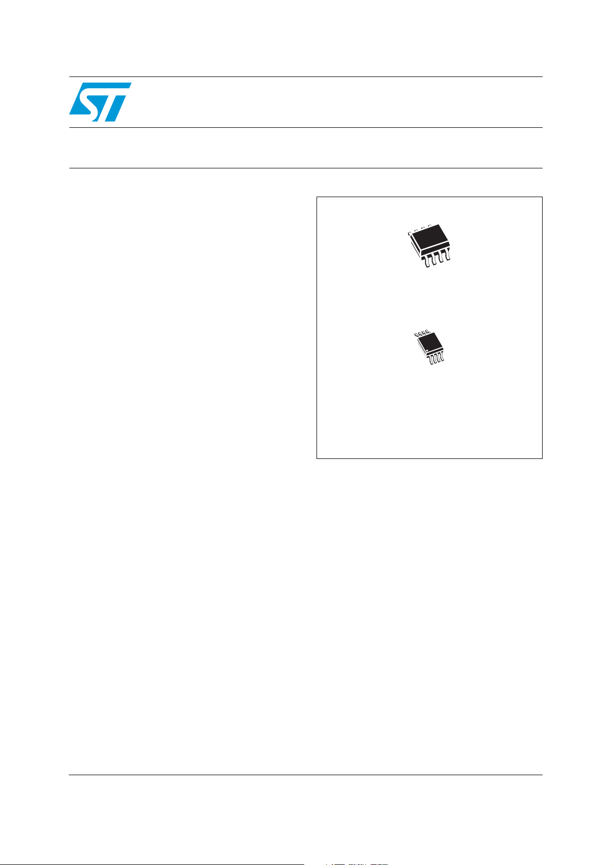
■ Packages:
–SO8
– MSOP8 (TSSOP8)
2
C/SMBus-compatible serial interface
connection of up to eight devices on the
same bus
STTS75
SO8
MSOP8 (TSSOP8)
June 2010 Doc ID 13298 Rev 11 1/41
www.st.com
1
Page 2

Contents STTS75
Contents
1 Description . . . . . . . . . . . . . . . . . . . . . . . . . . . . . . . . . . . . . . . . . . . . . . . . . 6
1.1 Serial communications . . . . . . . . . . . . . . . . . . . . . . . . . . . . . . . . . . . . . . . . 6
1.2 Temperature sensor output . . . . . . . . . . . . . . . . . . . . . . . . . . . . . . . . . . . . 6
1.3 Pin descriptions . . . . . . . . . . . . . . . . . . . . . . . . . . . . . . . . . . . . . . . . . . . . . 9
1.3.1 SDA (open drain) . . . . . . . . . . . . . . . . . . . . . . . . . . . . . . . . . . . . . . . . . . . 9
1.3.2 SCL . . . . . . . . . . . . . . . . . . . . . . . . . . . . . . . . . . . . . . . . . . . . . . . . . . . . . 9
1.3.3 OS
1.3.4 GND . . . . . . . . . . . . . . . . . . . . . . . . . . . . . . . . . . . . . . . . . . . . . . . . . . . . . 9
1.3.5 A2, A1, A0 . . . . . . . . . . . . . . . . . . . . . . . . . . . . . . . . . . . . . . . . . . . . . . . . 9
1.3.6 V
2 Operation . . . . . . . . . . . . . . . . . . . . . . . . . . . . . . . . . . . . . . . . . . . . . . . . . 10
2.1 Applications information . . . . . . . . . . . . . . . . . . . . . . . . . . . . . . . . . . . . . . 11
/INT (open drain) . . . . . . . . . . . . . . . . . . . . . . . . . . . . . . . . . . . . . . . . 9
DD . . . . . . . . . . . . . . . . . . . . . . . . . . . . . . . . . . . . . . . . . . . . . . . . . . . . . . . . . . . . . . . . . . . 9
2.2 Thermal alarm function . . . . . . . . . . . . . . . . . . . . . . . . . . . . . . . . . . . . . . 12
2.3 Comparator mode . . . . . . . . . . . . . . . . . . . . . . . . . . . . . . . . . . . . . . . . . . 12
2.4 Interrupt mode . . . . . . . . . . . . . . . . . . . . . . . . . . . . . . . . . . . . . . . . . . . . . 13
2.5 Fault tolerance . . . . . . . . . . . . . . . . . . . . . . . . . . . . . . . . . . . . . . . . . . . . . 14
2.6 Shutdown mode . . . . . . . . . . . . . . . . . . . . . . . . . . . . . . . . . . . . . . . . . . . . 14
2.7 Temperature data format . . . . . . . . . . . . . . . . . . . . . . . . . . . . . . . . . . . . . 15
2.8 Bus timeout feature . . . . . . . . . . . . . . . . . . . . . . . . . . . . . . . . . . . . . . . . . 15
2.9 One-shot mode . . . . . . . . . . . . . . . . . . . . . . . . . . . . . . . . . . . . . . . . . . . . . 16
3 Functional description . . . . . . . . . . . . . . . . . . . . . . . . . . . . . . . . . . . . . . 17
3.1 Registers and register set formats . . . . . . . . . . . . . . . . . . . . . . . . . . . . . . 17
3.1.1 Command/pointer register . . . . . . . . . . . . . . . . . . . . . . . . . . . . . . . . . . . 17
3.1.2 Configuration register . . . . . . . . . . . . . . . . . . . . . . . . . . . . . . . . . . . . . . 18
3.1.3 Temperature register . . . . . . . . . . . . . . . . . . . . . . . . . . . . . . . . . . . . . . . 19
3.1.4 Overlimit temperature register (T
3.1.5 Hysteresis temperature register (T
3.2 Power-up default conditions . . . . . . . . . . . . . . . . . . . . . . . . . . . . . . . . . . . 20
) . . . . . . . . . . . . . . . . . . . . . . . . . . . 19
OS
) . . . . . . . . . . . . . . . . . . . . . . . . . 20
HYS
3.3 Serial interface . . . . . . . . . . . . . . . . . . . . . . . . . . . . . . . . . . . . . . . . . . . . . 21
3.4 2-wire bus characteristics . . . . . . . . . . . . . . . . . . . . . . . . . . . . . . . . . . . . . 21
3.4.1 Bus not busy . . . . . . . . . . . . . . . . . . . . . . . . . . . . . . . . . . . . . . . . . . . . . 21
2/41 Doc ID 13298 Rev 11
Page 3

STTS75 Contents
3.4.2 Start data transfer . . . . . . . . . . . . . . . . . . . . . . . . . . . . . . . . . . . . . . . . . 21
3.4.3 Stop data transfer . . . . . . . . . . . . . . . . . . . . . . . . . . . . . . . . . . . . . . . . . 21
3.4.4 Data valid . . . . . . . . . . . . . . . . . . . . . . . . . . . . . . . . . . . . . . . . . . . . . . . . 22
3.4.5 Acknowledge . . . . . . . . . . . . . . . . . . . . . . . . . . . . . . . . . . . . . . . . . . . . . 23
3.5 READ mode . . . . . . . . . . . . . . . . . . . . . . . . . . . . . . . . . . . . . . . . . . . . . . . 24
3.6 WRITE mode . . . . . . . . . . . . . . . . . . . . . . . . . . . . . . . . . . . . . . . . . . . . . . 26
4 Typical operating characteristics . . . . . . . . . . . . . . . . . . . . . . . . . . . . . 28
5 Maximum ratings . . . . . . . . . . . . . . . . . . . . . . . . . . . . . . . . . . . . . . . . . . . 29
6 DC and AC parameters . . . . . . . . . . . . . . . . . . . . . . . . . . . . . . . . . . . . . . 30
7 Package mechanical data . . . . . . . . . . . . . . . . . . . . . . . . . . . . . . . . . . . . 33
8 Part numbering . . . . . . . . . . . . . . . . . . . . . . . . . . . . . . . . . . . . . . . . . . . . 38
9 Package marking information . . . . . . . . . . . . . . . . . . . . . . . . . . . . . . . . 39
10 Revision history . . . . . . . . . . . . . . . . . . . . . . . . . . . . . . . . . . . . . . . . . . . 40
Doc ID 13298 Rev 11 3/41
Page 4

List of tables STTS75
List of tables
Table 1. Signal names . . . . . . . . . . . . . . . . . . . . . . . . . . . . . . . . . . . . . . . . . . . . . . . . . . . . . . . . . . . . 7
Table 2. Fault tolerance setting . . . . . . . . . . . . . . . . . . . . . . . . . . . . . . . . . . . . . . . . . . . . . . . . . . . . 14
Table 3. Shutdown mode and one-shot mode description . . . . . . . . . . . . . . . . . . . . . . . . . . . . . . . . 14
Table 4. Relationship between temperature and digital output. . . . . . . . . . . . . . . . . . . . . . . . . . . . . 15
Table 5. Command/pointer register format . . . . . . . . . . . . . . . . . . . . . . . . . . . . . . . . . . . . . . . . . . . . 17
Table 6. Register pointers selection summary . . . . . . . . . . . . . . . . . . . . . . . . . . . . . . . . . . . . . . . . . 17
Table 7. Configuration register format . . . . . . . . . . . . . . . . . . . . . . . . . . . . . . . . . . . . . . . . . . . . . . . 18
Table 8. Programmable resolution configurations . . . . . . . . . . . . . . . . . . . . . . . . . . . . . . . . . . . . . . 18
Table 9. Temperature register format . . . . . . . . . . . . . . . . . . . . . . . . . . . . . . . . . . . . . . . . . . . . . . . . 19
Table 10. T
Table 11. STTS75 serial bus slave addresses . . . . . . . . . . . . . . . . . . . . . . . . . . . . . . . . . . . . . . . . . . 21
Table 12. Absolute maximum ratings . . . . . . . . . . . . . . . . . . . . . . . . . . . . . . . . . . . . . . . . . . . . . . . . . 29
Table 13. Operating and AC measurement conditions . . . . . . . . . . . . . . . . . . . . . . . . . . . . . . . . . . . . 30
Table 14. DC and AC characteristics . . . . . . . . . . . . . . . . . . . . . . . . . . . . . . . . . . . . . . . . . . . . . . . . . 31
Table 15. AC characteristics . . . . . . . . . . . . . . . . . . . . . . . . . . . . . . . . . . . . . . . . . . . . . . . . . . . . . . . . 32
Table 16. SO8 – 8-lead plastic small outline (4.90 mm x 3.90 mm) package mechanical data . . . . . 34
Table 17. MSOP8 (TSSOP8) – 8-lead, thin shrink small outline (3 mm x 3 mm) package
Table 18. Carrier tape dimensions for SO8 and MSOP8 (TSSOP8) packages . . . . . . . . . . . . . . . . . 36
Table 19. Reel dimensions for 12 mm carrier tape - SO8 and MSOP8 (TSSOP8) packages . . . . . . 37
Table 20. Ordering information scheme . . . . . . . . . . . . . . . . . . . . . . . . . . . . . . . . . . . . . . . . . . . . . . . 38
Table 21. Document revision history . . . . . . . . . . . . . . . . . . . . . . . . . . . . . . . . . . . . . . . . . . . . . . . . . 40
and T
OS
mechanical data . . . . . . . . . . . . . . . . . . . . . . . . . . . . . . . . . . . . . . . . . . . . . . . . . . . . . . . . . 35
register format . . . . . . . . . . . . . . . . . . . . . . . . . . . . . . . . . . . . . . . . . . . . . . . 20
HYS
4/41 Doc ID 13298 Rev 11
Page 5

STTS75 List of figures
List of figures
Figure 1. Logic diagram . . . . . . . . . . . . . . . . . . . . . . . . . . . . . . . . . . . . . . . . . . . . . . . . . . . . . . . . . . . . 7
Figure 2. Connections (SO8, TSSOP8) . . . . . . . . . . . . . . . . . . . . . . . . . . . . . . . . . . . . . . . . . . . . . . . . 8
Figure 3. Functional block diagram . . . . . . . . . . . . . . . . . . . . . . . . . . . . . . . . . . . . . . . . . . . . . . . . . . . 8
Figure 4. Typical 2-wire interface connection diagram . . . . . . . . . . . . . . . . . . . . . . . . . . . . . . . . . . . 11
Figure 5. OS
Figure 6. Serial bus data transfer sequence . . . . . . . . . . . . . . . . . . . . . . . . . . . . . . . . . . . . . . . . . . . 22
Figure 7. Acknowledgement sequence . . . . . . . . . . . . . . . . . . . . . . . . . . . . . . . . . . . . . . . . . . . . . . . 23
Figure 8. Slave address location . . . . . . . . . . . . . . . . . . . . . . . . . . . . . . . . . . . . . . . . . . . . . . . . . . . . 24
Figure 9. Typical 2-byte READ from preset pointer location (e.g. temp - T
Figure 10. Typical pointer set followed by an immediate READ for 2-byte register (e.g. temp). . . . . . 25
Figure 11. Typical 1-byte READ from the configuration register with preset pointer . . . . . . . . . . . . . . 25
Figure 12. Typical pointer set followed by an immediate READ from the configuration register . . . . . 26
Figure 13. Configuration register WRITE . . . . . . . . . . . . . . . . . . . . . . . . . . . . . . . . . . . . . . . . . . . . . . . 26
Figure 14. T
Figure 15. Temperature variation vs. voltage . . . . . . . . . . . . . . . . . . . . . . . . . . . . . . . . . . . . . . . . . . . 28
Figure 16. Bus timing requirements sequence . . . . . . . . . . . . . . . . . . . . . . . . . . . . . . . . . . . . . . . . . . 32
Figure 17. SO8 – 8-lead plastic small outline (4.90 mm x 3.90 mm) package mechanical drawing . . 34
Figure 18. MSOP8 (TSSOP8) – 8-lead, thin shrink small outline (3 mm x 3 mm) package
Figure 19. Carrier tape for SO8 and MSOP8 (TSSOP8) packages . . . . . . . . . . . . . . . . . . . . . . . . . . . 36
Figure 20. Reel schematic . . . . . . . . . . . . . . . . . . . . . . . . . . . . . . . . . . . . . . . . . . . . . . . . . . . . . . . . . . 37
Figure 21. Device topside marking information (SO8) . . . . . . . . . . . . . . . . . . . . . . . . . . . . . . . . . . . . . 39
Figure 22. Device topside marking information (MSOP8/TSSOP8). . . . . . . . . . . . . . . . . . . . . . . . . . . 39
output temperature response diagram . . . . . . . . . . . . . . . . . . . . . . . . . . . . . . . . . . . . . 13
, T
) . . . . . . . . . . . . 25
HYS
OS
and T
OS
WRITE. . . . . . . . . . . . . . . . . . . . . . . . . . . . . . . . . . . . . . . . . . . . . . . . . . . . . 27
HYS
mechanical drawing . . . . . . . . . . . . . . . . . . . . . . . . . . . . . . . . . . . . . . . . . . . . . . . . . . . . . . 35
Doc ID 13298 Rev 11 5/41
Page 6

Description STTS75
1 Description
The STTS75 is a high-precision CMOS (digital) temperature sensor IC with a delta-sigma
analog-to-digital (ADC) converter and an I
for general applications such as personal computers, system thermal management,
electronics equipment, and industrial controllers, and is packaged in the industry standard
8-lead MSOP(TSSOP) and SO8 packages.
The device contains a band gap temperature sensor and programmable 9- to 12-bit ADC
which monitor and digitize the temperature to a resolution up to 0.0625 °C. The STTS75 is
typically accurate to (±3 °C - max) over the full temperature measurement range of
–55 °C to 125 °C with ±2 °C accuracy in the –25 °C to +100 °C range. At power-up, the
STTS75 defaults to 9-bit resolution for software compatibility with the STLM75.
The STTS75 is specified for operating at supply voltages from 2.7 V to 5.5 V. Operating at
3.3 V, the supply current is typically (75 µA).
The onboard delta-sigma analog-to-digital converter (ADC) converts the measured
temperature to a digital value that is calibrated in °C; for Fahrenheit applications a lookup
table or conversion routine is required.
The STTS75 is factory-calibrated and requires no external components to measure
temperature.
1.1 Serial communications
The STTS75 has a simple 2-wire I2C-compatible digital serial interface which allows the
user to access the data in the temperature register at any time. It communicates via the
serial interface with a master controller which operates at speeds up to 400 kHz. Three pins
(A0, A1, and A2) are available for address selection, and enable the user to connect up to 8
devices on the same bus without address conflict.
2
C-compatible serial digital interface. It is targeted
In addition, the serial interface gives the user easy access to all STTS75 registers to
customize operation of the device.
1.2 Temperature sensor output
The STTS75 temperature sensor has a dedicated open drain overlimit signal/alert
(OS
/INT/Alert) output which features a thermal alarm function. This function provides a
user-programmable trip and turn-off temperature. It can operate in either of two selectable
modes:
● Section 2.3: Comparator mode, and
● Section 2.4: Interrupt mode.
At power-up the STTS75 comes up in 9-bit mode and immediately begins measuring the
temperature and converting the temperature to a digital value. The resolution of the digital
output data is user-configurable to 9, 10, 11, or 12 bits which correspond to temperature
increments of 0.5 °C, 0.25 °C, 0.125 °C, and 0.0625 °C, respectively.
6/41 Doc ID 13298 Rev 11
Page 7
STTS75 Description
The measured temperature value is compared with a temperature limit (which is stored in
the 16-bit (T
the 16-bit (T
OS
/INT pin is activated (see Figure 3 on page 8).
) READ/WRITE register), and the hysteresis temperature (which is stored in
OS
) READ/WRITE register). If the measured value exceeds these limits, the
HYS
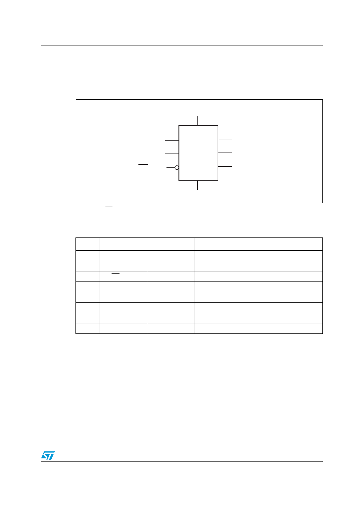
Figure 1. Logic diagram
V
DD
(1)
SDA
SCL
O.S./INT
1. SDA and OS/INT are open drain.
(1)
Note: See Pin descriptions on page 9 for details.
Table 1. Signal names
Pin Symbol/name Type/direction Description
DD
(1)
(1)
2
1
0
Input/output Serial data input/output
Output Overlimit signal/interrupt alert output
Input Address2 input
Input Address1 input
Input Address0 input
Supply power Supply voltage (2.7 V to 5.5 V)
1SDA
2 SCL Input Serial clock input
3OS/INT
4 GND Supply ground Ground
5A
6A
7A
8V
1. SDA and OS/INT are open drain.
STTS75
GND
A
0
A
1
A
2
AI11840
Note: See Pin descriptions on page 9 for details.
Doc ID 13298 Rev 11 7/41
Page 8
Description STTS75
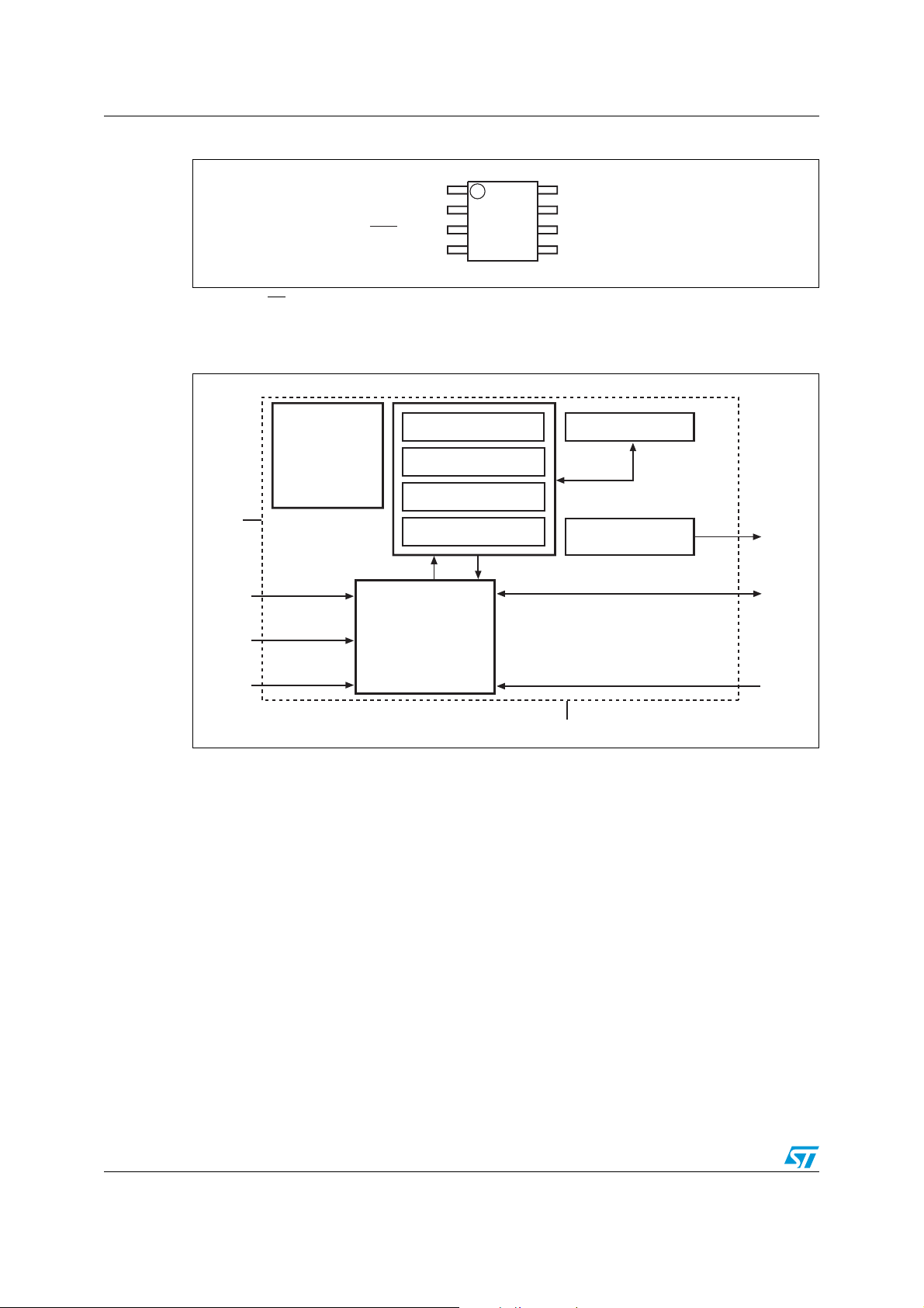
Figure 2. Connections (SO8, TSSOP8)
(1)
O.S./INT
1. SDA and OS/INT are open drain.
SDA
GND
SCL
(1)
1
2
3
4
V
8
7
6
5
DD
A
0
A
1
A
2
AI11841
Note: See Pin descriptions on page 9 for details.
Figure 3. Functional block diagram
Temperature
Sensor and
Analog-to-Digital
Converter (ADC)
Σ-Δ
V
DD
A
0
A
1
A
2
Configuration Register
Temperature Register
THYS Set Point Register
TOS Set Point Register
2-wire I2C Interface
Pointer Register
Control and Logic
Comparator
GND
O.S.
SDA
SCL
AI11833a
8/41 Doc ID 13298 Rev 11
Page 9

STTS75 Description
1.3 Pin descriptions
See Figure 1 on page 7 and Table 1 on page 7 for a brief overview of the signals connected
to this device.
1.3.1 SDA (open drain)
This is the serial data input/output pin for the 2-wire serial communication port.
1.3.2 SCL
This is the serial clock input pin for the 2-wire serial communication port.
1.3.3 OS/INT (open drain)
This is the overlimit signal/interrupt alert output pin. It is open drain, so it needs a pull-up
resistor.
Note: The open drain thermostat output that indicates if the temperature has exceeded user-
programmable limits (over/under temperature indicator).
1.3.4 GND
Ground; it is the reference for the power supply. It must be connected to system ground.
1.3.5 A2, A1, A0
A2, A1, and A0 are selectable address pins for the 3LSBs of the I2C interface address. They
can be set to V
1.3.6 V
DD
This is the supply voltage pin and ranges from +2.7 V to +5.5 V.
or GND to provide 8 unique address selections.
DD
Doc ID 13298 Rev 11 9/41
Page 10

Operation STTS75
2 Operation
After each temperature measurement and analog-to-digital conversion, the STTS75 stores
the temperature as a 16-bit two’s complement number in the 2-byte temperature register.
The most significant bit (S, bit 15) indicates if the temperature is positive or negative:
● for positive numbers S = 0, and
● for negative numbers S = 1.
The most recently converted digital measurement can be read from the temperature register
at any time. Since temperature conversions are performed in the background, reading the
temperature register does not affect the operation in progress.
Bits 3 through 0 of the temperature register are hardwired to logic '0.' When the STTS75 is
configured for 12-bit resolution, the 12 MSBs (bits 15 through 4) of the temperature register
will contain temperature data. For 11-bit resolution, the 11 MSBs (bits 15 through 5) of the
temperature register will contain data, and bit 4 will read out as logic '0.' For 10-bit
resolution, the 10 MSBs (bits 15 through 6) will contain data, and for 9-bit resolution the
9 MSBs (bits 15 through 7) will contain data and all unused LSBs will contain '0s.'
Table 4 on page 15 gives examples of 12-bit resolution digital output data and the
corresponding temperatures. The data is compared to the values in the T
registers, and then the OS
operating mode. The number of T
/INT is updated based on the result of the comparison and the
OS
and T
bits used during the thermostat comparison
HYS
is equal to the conversion resolution set by the FT1 and FT0 bits in the configuration
register. For example, if the resolution is 9 bits, only the 9 MSBs of T
OS
used by the thermostat comparator. The alarm fault tolerance is controlled by the FTI and
FTO bits in the configuration register. They are used to set up a fault queue. This prevents
false tripping of the OS
/INT pin when the STTS75 is used in a noisy environment (see
Table 2 on page 14).
OS
and T
and T
HYS
HYS
will be
The STTS75 also supports a special one-shot mode feature that performs a single
temperature measurement and returns to shutdown mode. This is especially useful for lowpower applications. This features is accessed by first putting the device in shutdown mode,
then enabling the one-shot mode (OSM) bit in the configuration register.
The active state of the OS
/INT output can be changed via the polarity (POL) bit in the
configuration register. The power-up default is active-low.
If the user does not wish to use the thermostat capabilities of the STTS75, the OS
output should be left floating.
Note: If the thermostat is not used, the T
system data.
OS
and T
/INT
registers can be used for general storage of
HYS
10/41 Doc ID 13298 Rev 11
Page 11
STTS75 Operation
2.1 Applications information
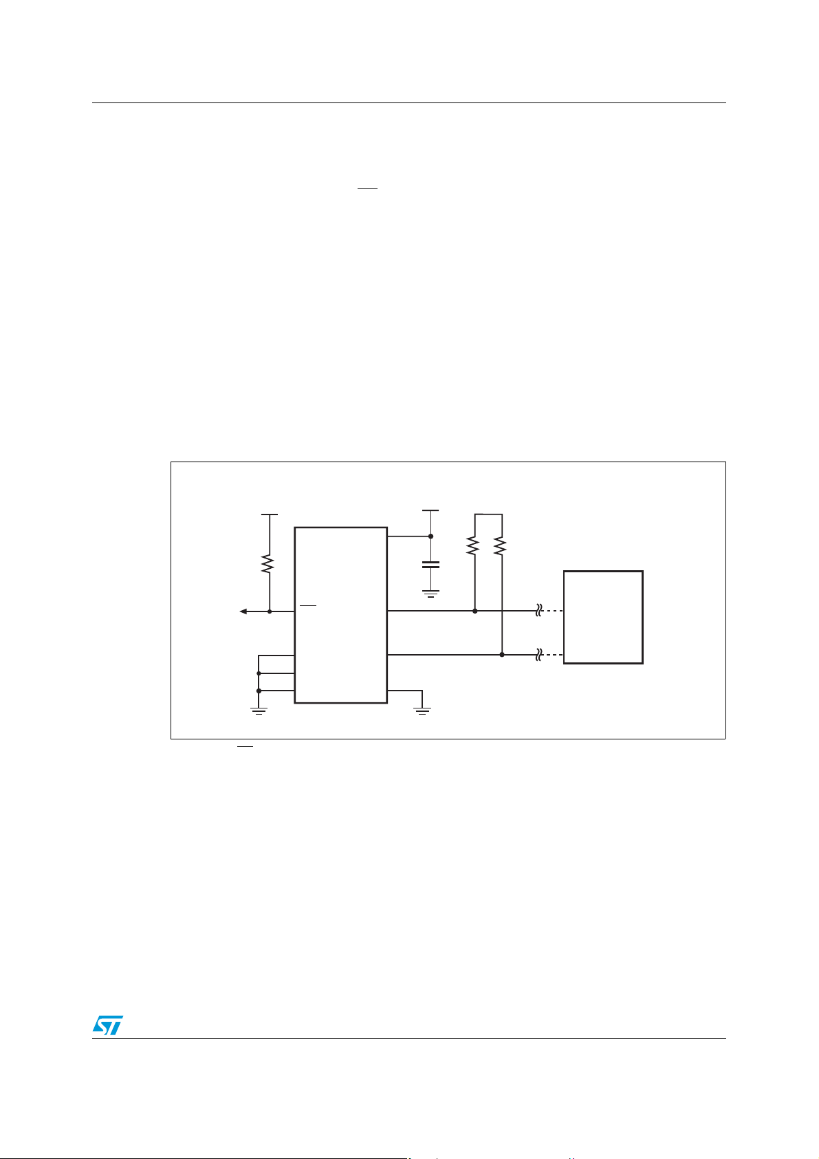
STTS75 digital temperature sensors are optimal for thermal management and thermal
protection applications. They require no external components for operations except for pullup resistors on SCL, SDA, and OS
The sensing device of STTS75 is the chip itself. The typical interface connection for this type
of digital sensor is shown in Figure 4 on page 11.
Intended applications include:
● System thermal management
● Computers/disk drivers
● Electronics/test equipment
● Power supply modules
● Consumer products
● Battery management
● Fax/printers management
● Automotive
Figure 4. Typical 2-wire interface connection diagram
/INT outputs. A 0.1 µF bypass capacitor is recommended.
Pull-up
V
DD
10kΩ
1. SDA and OS/INT are open drain.
STTS75
O.S./INT
A
0
A
1
A
2
(1)
SDA
V
DD
SCL
(1)
GND
0.1μF
V
DD
Pull-up
V
10kΩ 10kΩ
I2C Address = 1001000 (1001A2A1A0)
DD
Master
Device
AI11832
Doc ID 13298 Rev 11 11/41
Page 12

Operation STTS75
2.2 Thermal alarm function
The STTS75 thermal alarm function provides user-programmable thermostat capability and
allows the STTS75 to function as a standalone thermostat without using the serial interface.
The OS
/INT output is the alarm output. This signal is an open drain output, and at power-up,
this pin is configured with active-low polarity by default.
2.3 Comparator mode
In comparator mode, each time a temperature-to-digital (T-to-D) temperature conversion
occurs, the new digital temperature is compared to the value stored in the T
registers. If a fault tolerance number of consecutive temperature measurements are greater
than the value stored in the T
register, the OS/INT output will be activated.
OS
For example, if the FT1 and FT0 bits are equal to “10” (fault tolerance = 4), four consecutive
temperature measurements must exceed T
OS
/INT output is active, it will remain active until the first time the measured temperature
drops below the temperature stored in the T
When the thermostat is in comparator mode, the OS
with any amount of hysteresis. The OS
temperature exceeds the T
value a consecutive number of times as defined by the FT1
OS
/INT output becomes active when the measured
and FT0 fault tolerance (FT) bits in the configuration register. The OS
when the temperature falls below the value stored in T
to activate the OS/INT output. Once the
OS
register.
HYS
/INT can be programmed to operate
/INT then stays active
register for a consecutive number
HYS
of times as defined by the fault tolerance bits (FT1 and FT0). Putting the device into
shutdown mode does not clear OS
/INT in comparator mode.
OS
and T
HYS
12/41 Doc ID 13298 Rev 11
Page 13
STTS75 Operation
2.4 Interrupt mode
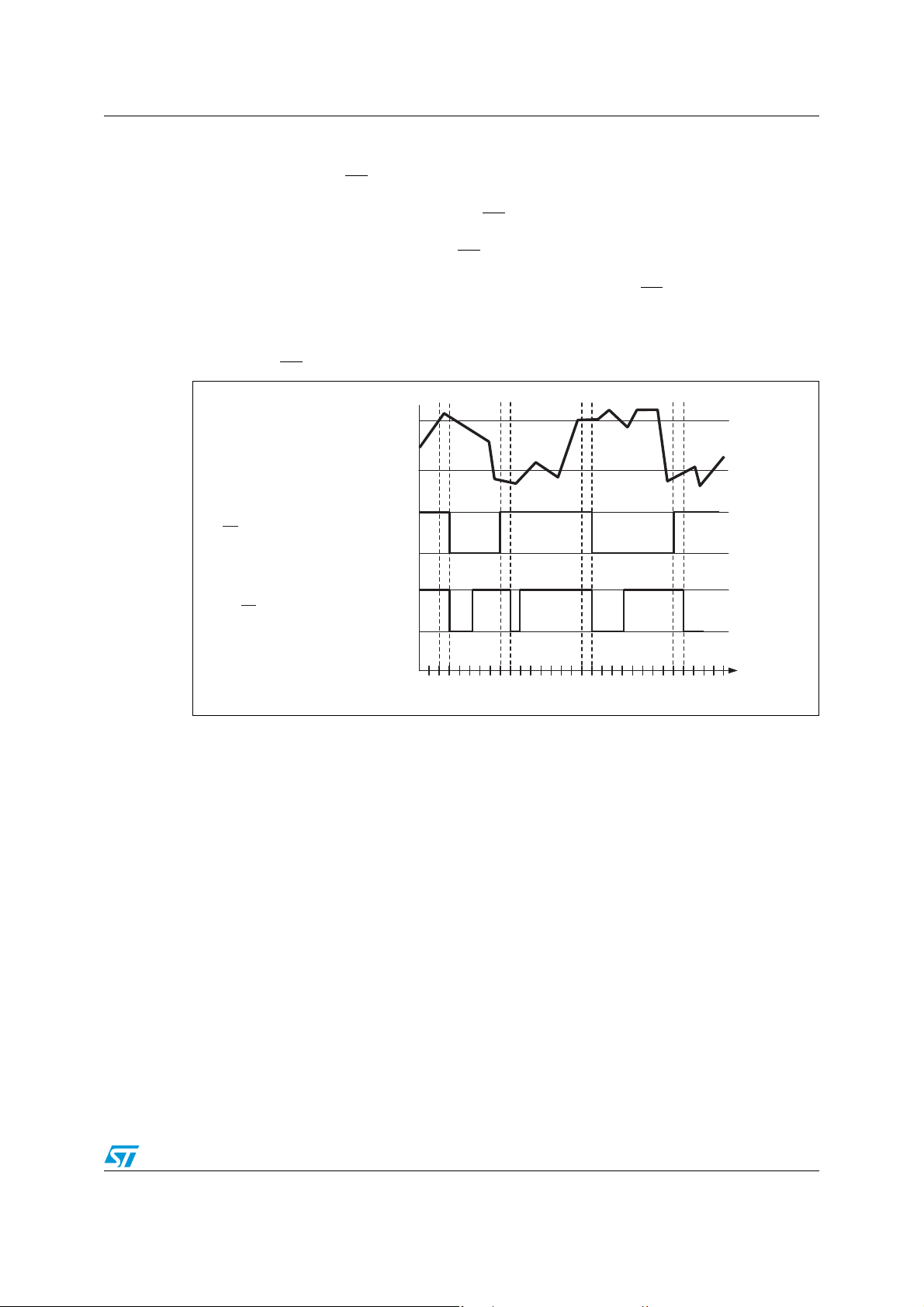
In Interrupt mode, the OS/INT output first becomes active when the measured temperature
exceeds the T
configuration register. Once activated, the OS
STTS75 into shutdown mode or by reading from any register (temperature, configuration,
T
, or T
OS
HYS
reactivated when the measured temperature falls below the T
number of times equal to the FT value. Figure 5 illustrates typical OS
response for STTS75 configured to have a fault tolerance of 2. The interrupt/clear process is
cyclical between T
value a consecutive number of times equal to the FT value in the
OS
/INT can only be cleared by either putting the
) on the device. Once the OS/INT has been deactivated, it will only be
value a consecutive
HYS
output temperature
OS
and T
HYS
.
Figure 5. OS
output temperature response diagram
T
OS
Temperature
T
HYS
Inactive
OS Output - Comparator mode
Active
Inactive
OS Output - Interrupt mode
Active
(1)(1)
(1)
Conversions
1. This assumes that a READ has occurred.
Note: The STTS75 is configured to have a fault tolerance of 2 in this example.
AI12224b
Doc ID 13298 Rev 11 13/41
Page 14
Operation STTS75
2.5 Fault tolerance
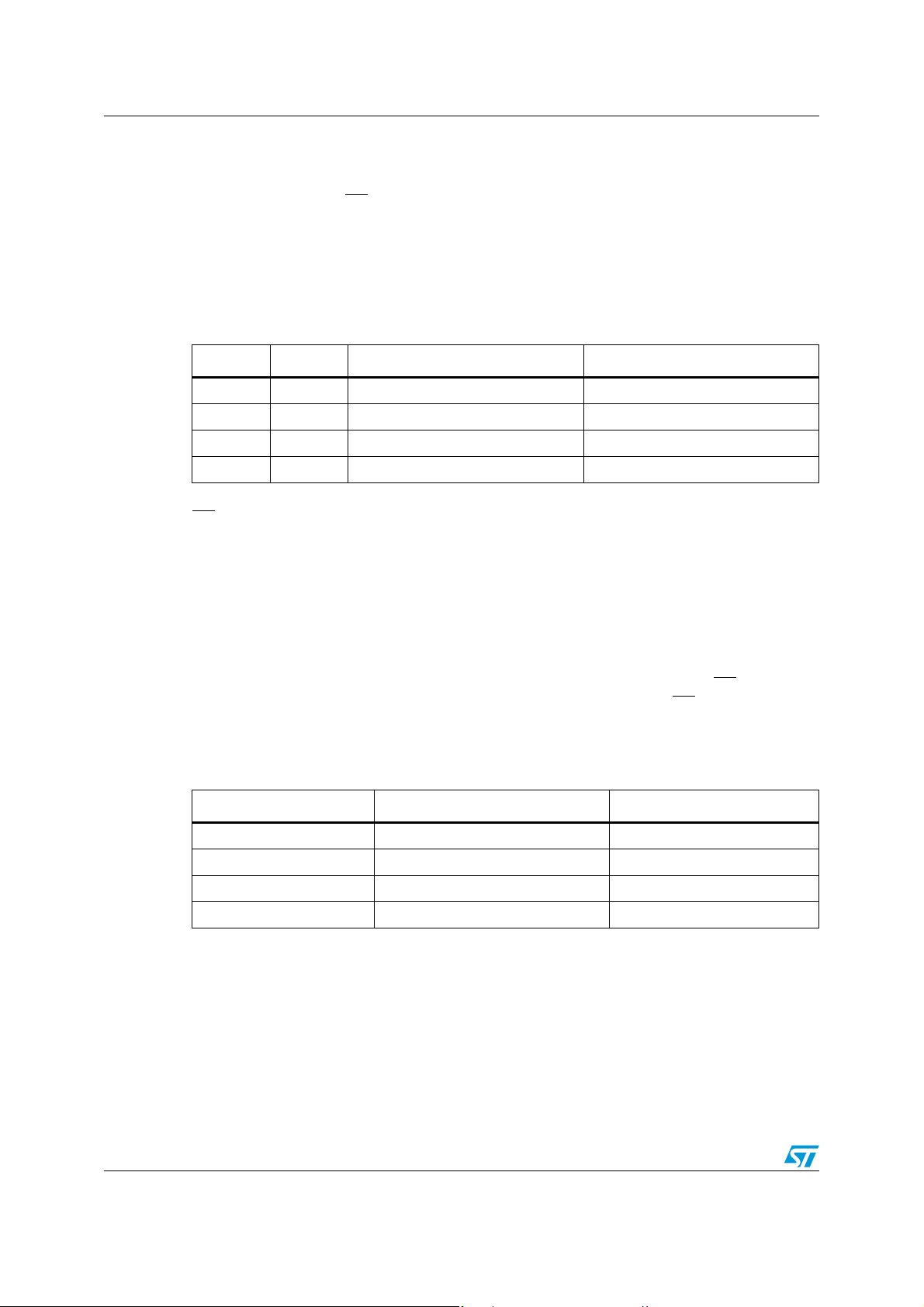
For both comparator and interrupt modes, the alarm “fault tolerance” setting plays a role in
determining when the OS
of consecutive times an error condition must be detected before the user is notified. Higher
fault tolerance settings can help eliminate false alarms caused by noise in the system. The
alarm fault tolerance is controlled by the bits (bits 4 and 3) in the configuration register.
These bits can be used to set the fault tolerance to 1, 2, 4, or 6 as shown in Tab le 2 . At
power-up, these bits both default to logic '0.'
Table 2. Fault tolerance setting
FT1 FT0 STTS75 (consecutive faults) Comments
0 0 1 Power-up default
01 2
10 4
11 6
/INT output will be activated. Fault tolerance refers to the number
Note: OS output will be asserted one t
condition remains.
2.6 Shutdown mode
For power-sensitive applications, the STTS75 offers a low-power shutdown mode. The SD
bit in the configuration register controls shutdown mode. When SD is changed to login '1,'
the conversion in progress will be completed and the result stored in the temperature
register, after which the STTS75 will go into a low-power standby state. The OS
will be cleared if the thermostat is operating in Interrupt mode and the OS
unchanged in comparator mode. The 2-wire interface remains operational in shutdown
mode, and writing a '0' to the SD bit returns the STTS75 to normal operation.
Table 3. Shutdown mode and one-shot mode description
Operational mode One-shot mode (OSM) (bit 7) Shutdown (SD) (bit 0)
Continuous conversion 0 0
Shutdown
Continuous conversion 1 0
One-shot 1 1
1. The shutdown command needs to be programmed before sending a one-shot command.
(1)
after fault tolerance is met, provided that the error
CONV
/INT will remain
01
/INT output
14/41 Doc ID 13298 Rev 11
Page 15
STTS75 Operation
2.7 Temperature data format
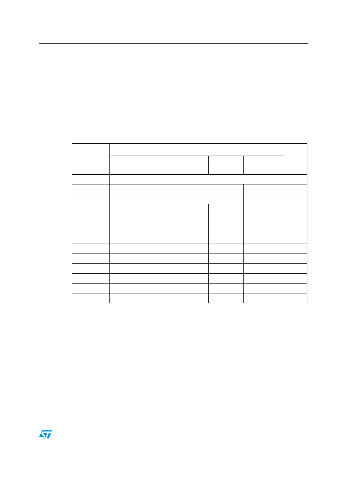
Ta bl e 4 shows the relationship between the output digital data and the external temperature
for 12-bit resolution.
Temperature data for temperature, T
OS
and T
registers is represented by 9-bit, 10-bit,
HYS
11-bit, and 12-bit depending upon the resolution bits RC1, RC0 (bits 6 and 5) in the
configuration register (see Table 7 on page 18). The default resolution is 9-bit.
The left-most bit in the output data stream controls temperature polarity information for each
conversion. If the sign bit is '0', the temperature is positive and of the sign bit is '1', the
temperature is negative.
Table 4. Relationship between temperature and digital output
Digital
Temperature
+125 °C 0 111 1101 0 0 0 0 0000 7D00
+25.0625 °C 0 001 1001 0 0 0 1 0000 1910
+10.125 °C 0 000 1010 0 0 1 0 0000 0A20
+0.5 °C 0 000 0000 1 0 0 0 0000 0080
0°C 0 000 0000 0 0 0 0 0000 0000
–0.5 °C 1 111 1111 1 0 0 0 0000 FF80
Number of bits used by
Sign
conversion resolution
10-bit resolution 0 0 0000
9-bit resolution 0 0 0 0000
9101112
12-bit resolution 0000
11-bit resolution 0 0000
Always
zero
output
(HEX)
–10.25 °C 1 111 0101 1 1 1 0 0000 F5E0
–25.0625 °C 1 110 0110 1 1 1 1 0000 E6F0
–55 °C 1 100 1001 0 0 0 0 0000 C900
2.8 Bus timeout feature
The STTS75 supports an SMBus-compatible timeout function which will reset the serial
2
I
C/SMBus interface if SDA is held low for a period greater than the timeout duration
between a START and STOP condition. If this occurs, the device will release the bus and
wait for another START condition.
Doc ID 13298 Rev 11 15/41
Page 16

Operation STTS75
2.9 One-shot mode
STTS75 supports a one-shot temperature measurement mode. This is invoked by putting
the device in shutdown mode (SD bit 0 in the configuration register is set to ‘1’) and writing a
‘1’ to the OSM (bit 7) to start a single temperature conversion. STTS75 returns to the
shutdown state after completion of the single conversion. This is useful to reduce power
consumption when continuous monitoring is not needed. When the configuration register is
read, the OSM bit will read ‘0’.
16/41 Doc ID 13298 Rev 11
Page 17
STTS75 Functional description
3 Functional description
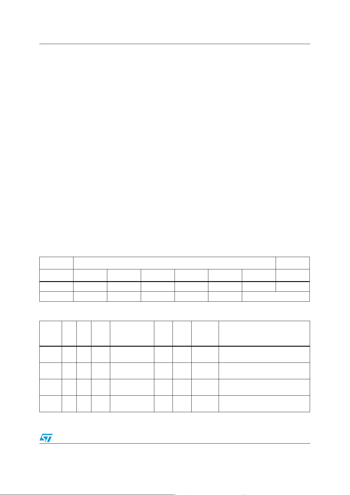
The STTS75 registers have unique pointer designations which are defined in Tab l e 6 o n
page 17. Whenever any READ/WRITE operation to the STTS75 register is desired, the user
must “point” to the device register to be accessed.
All of these user-accessible registers can be accessed via the digital serial interface at
anytime (see Serial interface on page 21), and they include:
● Command register/address pointer register
● Configuration register
● Temperature register
● Overlimit signal temperature register (T
● Hysteresis temperature register (T
HYS
3.1 Registers and register set formats
3.1.1 Command/pointer register
The most significant bits (MSBs) of the command register must always be zero. Writing a '1'
into any of these bits will cause the current operation to be terminated (see Ta b le 5 ).
)
OS
)
The command register retains pointer information between operations. Therefore, this
register only needs to be updated once for consecutive READ operations from the same
register. All bits in the command register default to '0' at power-up.
Table 5. Command/pointer register format
MSB LSB
Bit7 Bit6 Bit5 Bit4 Bit3 Bit2 Bit1 Bit0
000000P1P0
Table 6. Register pointers selection summary
Pointer
value
(H)
00 0 0 TEMP
01 0 1 CONF
02 1 0 T
P1 P0 Name Description
Temperature
register
Configuration
register
HYS
Hysteresis
register
Width
(bits)
Type
Power-on
(R/W)
Read
16
only
8R/W 00
16 R/W 4800 Default = 75 °C
default
N/A To store measured temperature data
Pointer
Comments
03 1 1 T
Overtemperature
OS
shutdown
16 R/W 5000
Doc ID 13298 Rev 11 17/41
Set point for overtemperature
shutdown (T
) limit default = 80 °C
OS
Page 18
Functional description STTS75
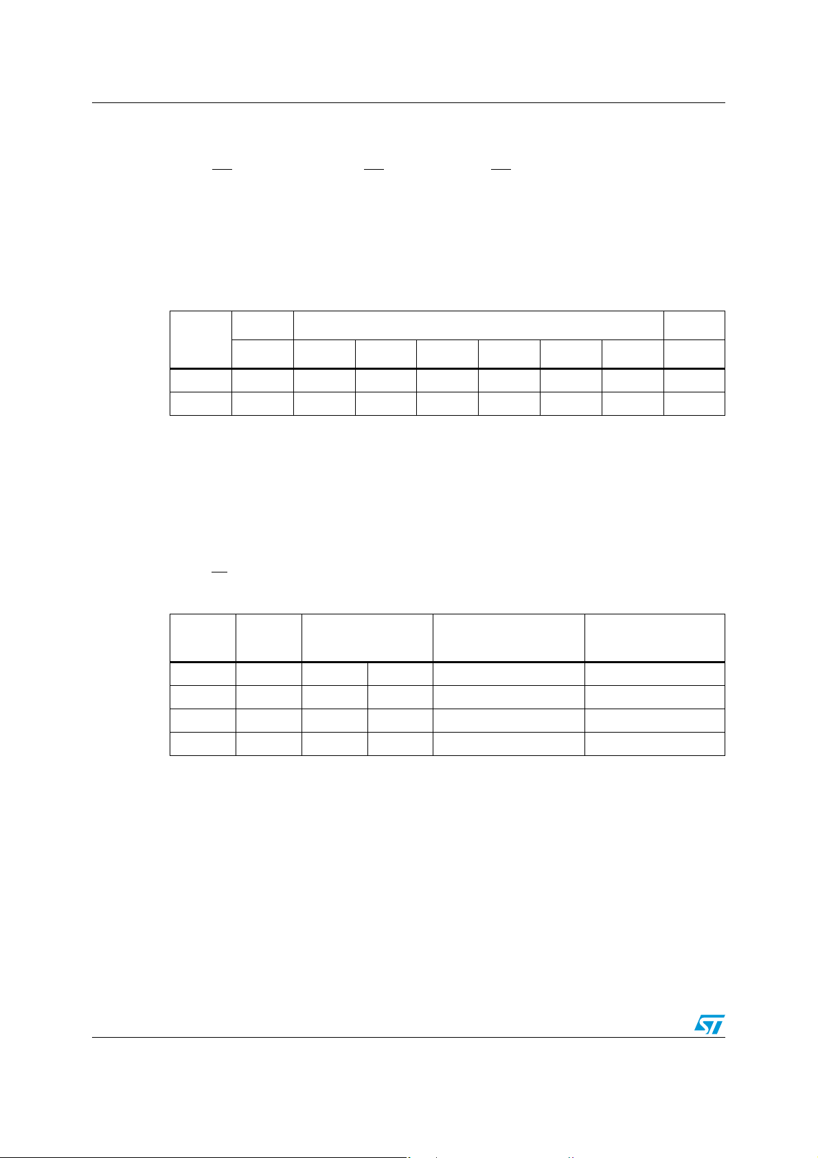
3.1.2 Configuration register
The configuration register is used to store the device settings such as device operation
mode, OS
The configuration register allows the user to program various options such as conversion
resolution (see Ta b le 8 ), thermostat fault tolerance, thermostat polarity, thermostat operating
mode, and shutdown mode. The user has READ/WRITE access to all of the bits in the
configuration register. The entire register is volatile and thus powers up in its default state
only.
Table 7. Configuration register format
Byte
STTS75 OSM RC1 RC0 FT1 FT0 POL M SD
Default00000000
Keys: SD = shutdown control bit FT1 = fault tolerance1 bit
1. Indicates operation mode; 0 = comparator mode, and 1 = interrupt mode (see Comparator mode and
Interrupt mode on page 13).
2. The OS/INT is active-low ('0').
Table 8. Programmable resolution configurations
/INT operation mode, OS/INT polarity, and OS/INT fault queue.
MSB LSB
Bit7 Bit6 Bit5 Bit4 Bit3 Bit2 Bit1 Bit0
(2)
(1)
RC0 = resolution conversion0 bit
RC1 = resolution conversion1 bit
M = thermostat mode
POL = output polarity
FT0 = fault tolerance0 bit OSM = one-shot mode bit
RC1 RC0 Resolution
Conversion time
(max)
Remarks
0 0 9-bit 0.5 °C 85 ms Default resolution
0 1 10-bit 0.25 °C 170 ms
1 0 11-bit 0.125 °C 340 ms
1 1 12-bit 0.0625 °C 680 ms
18/41 Doc ID 13298 Rev 11
Page 19
STTS75 Functional description
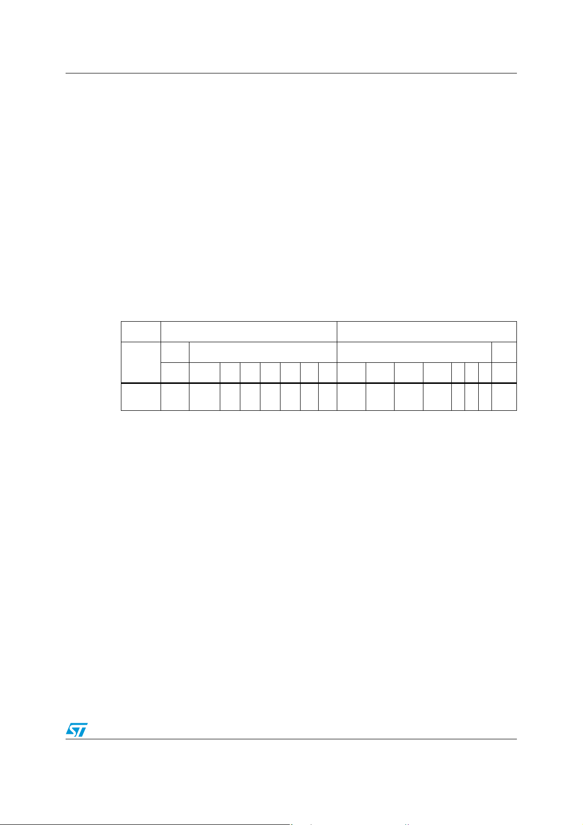
3.1.3 Temperature register
The temperature register is a two-byte (16-bit) “Read only” register (see Table 9 on
page 19). Digital temperatures from the ADC are stored in the temperature register in two’s
complement format, and the contents of this register are updated each time the A/D
conversion is finished.
The user can read data from the temperature register at any time. When a T-to-D conversion
is completed, the new data is loaded into a comparator buffer to evaluate fault conditions
and will update the temperature register if a read cycle is not ongoing. If a READ is ongoing,
the previous temperature will be read. Accessing the STTS75 continuously without waiting
at least one conversion time between communications will prevent the device from updating
the temperature register with a new temperature conversion result. Consequently, the
STTS75 should not be accessed continuously with a wait time of less than t
Depending on the A/D conversion resolution, the 9-, 10-, 11- or 12-bit MSBs of the register
will contain temperature data. All unused bits following the digital temperature will be zero.
The MSB (bit 15) of the temperature register denotes whether the temperature data is
positive or negative. A '0' in bit 15 is positive and a '1' is negative.
Table 9. Temperature register format
Bytes MS byte LS byte
CONV
(max).
MSB THSB TLSB LSB
Bits
15 14 13 12 11 10 9 8 7 6 5 4 3 2 1 0
STTS75 SB TMSB TD TD TD TD TD TD
Keys: SB = two’s complement sign bit
TMSB = temperature MSB
TLSB = temperature LSB
TD = temperature data
3.1.4 Overlimit temperature register (TOS)
The TOS register is a two-byte (16-bit) READ/WRITE register that stores the userprogrammable upper trip-point temperature for the thermal alarm in two’s complement
format (see Table 10 on page 20). This register defaults to 80 °C at power-up (i.e., 0101
0000 0000 0000).
The format of the T
the T
register are hardwired to zero, so data written to these register bits will be ignored.
OS
The MSB position contains the sign bit for the digital temperature and bit14 contains the
temperature MSB.
register is identical to that of the temperature register. The 4 LSBs of
OS
9-bit
LSB
10-bit
LSB
11-bit
LSB
12-bit
LSB
000 0
The resolution setting for the A/D conversion determines how many bits of the T
register
OS
are used by the thermal alarm. For example, for 9-bit conversions, the trip-point temperature
is defined by the 9 MSBs of the T
register, and all remaining bits are “Don’t cares.”
OS
Doc ID 13298 Rev 11 19/41
Page 20
Functional description STTS75
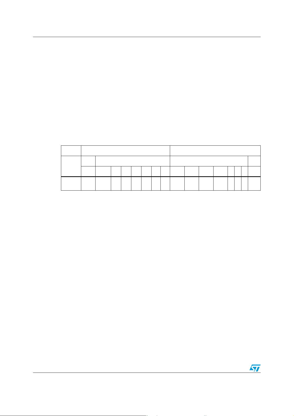
3.1.5 Hysteresis temperature register (T
T
register is a two-byte (16-bit) READ/WRITE register that stores the user-
HYS
programmable lower trip-point temperature for the thermal alarm in two’s complement
format (see Ta bl e 1 0 ). This register defaults to 75 °C at power-up (i.e., 0100 1011 0000
0000).
The format of this register is the same as that of the temperature register. The 4 LSBs of the
T
register are hardwired to zero, so data written to these bits is ignored. The MSB
HYS
position contains the sign bit for the digital temperature and bit 14 contains the temperature
MSB.
The resolution setting for the A/D conversion determines how many bits of the T
are used by the thermal alarm. For example, for 9-bit conversions, the hysteresis
temperature is defined by the 9 MSBs of the T
cares.”
Table 10. T
Bytes MS byte LS byte
Bits
STTS75 SB TMSB TD TD TD TD TD TD
and T
OS
MSB THSB TLSB LSB
15 14 13 12 11 10 9 8 7 6 5 4 3 2 1 0
register format
HYS
)
HYS
register, and all remaining bits are “Don’t
HYS
9-bit
10-bit
11-bit
12-bit
LSB
LSB
LSB
LSB
000 0
HYS
register
Keys: SB = two’s complement sign bit
TMSB = temperature MSB
TLSB = temperature LSB
TD = temperature data
3.2 Power-up default conditions
The STTS75 always powers up in the following default states:
● Thermostat mode = comparator mode
● Polarity = active-low
● Fault tolerance = 1 fault (i.e., relevant bits set to '0' in the configuration register)
● T
● T
● OSM = 0 (disabled)
● Register pointer = 00 (temperature register)
● Conversion resolution = 9-bit (i.e., RC0 = 0 and RC1 = 0 in the configuration register;
Note: After power-up these conditions can be reprogrammed via the serial interface.
= 80 °C
OS
= 75 °C
HYS
see Table 7 on page 18)
20/41 Doc ID 13298 Rev 11
Page 21
STTS75 Functional description
3.3 Serial interface
Writing to and reading from the STTS75 registers is accomplished via the two-wire serial
interface protocol which requires that one device on the bus initiates and controls all READ
and WRITE operations. This device is called the “master” device. The master device also
generates the SCL signal which provides the clock signal for all other devices on the bus.
These other devices on the bus are called “slave” devices. The STTS75 is a slave device
(see Ta bl e 11 ). Both the master and slave devices can send and receive data on the bus.
During operations, one data bit is transmitted per clock cycle. All operations follow a
repeating, nine-clock-cycle pattern that consists of eight bits (one byte) of transmitted data
followed by an acknowledge (ACK) or not acknowledge (NACK) from the receiving device.
Note: There are no unused clock cycles during any operation, so there must not be any breaks in
the data stream and ACKs/NACKs during data transfers. Conversely, having too few clock
cycles can lead to incorrect operation if an inadvertent 8-bit READ from a 16-bit register
occurs.
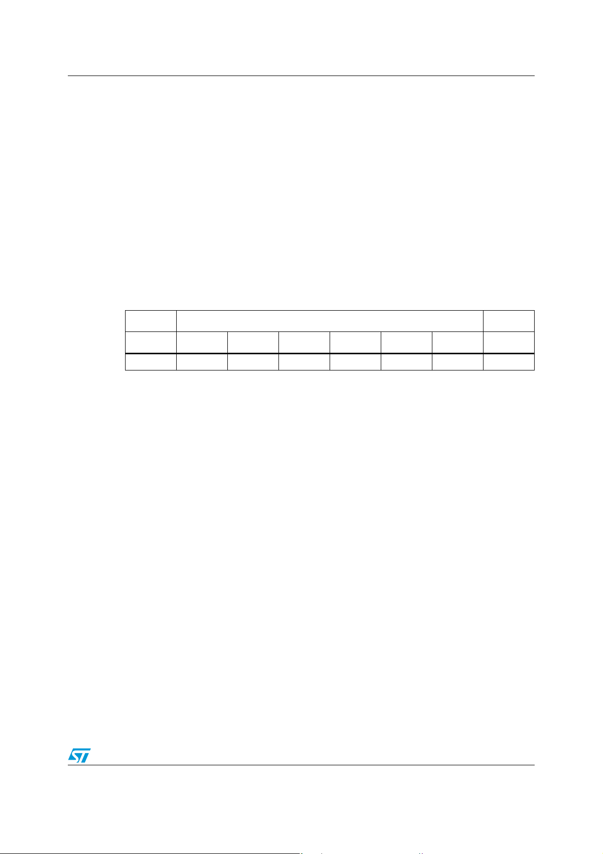
Table 11. STTS75 serial bus slave addresses
MSB LSB
Bit7 Bit6 Bit5 Bit4 Bit3 Bit2 Bit1 Bit0
1 0 0 1 A2 A1 A0 R/W
3.4 2-wire bus characteristics
The bus is intended for communication between different ICs. It consists of two lines: a bidirectional data signal (SDA) and a clock signal (SCL). Both the SDA and SCL lines must be
connected to a positive supply voltage via a pull-up resistor.
● The following protocol has been defined:
● Data transfer may be initiated only when the bus is not busy.
● During data transfer, the data line must remain stable whenever the clock line is high.
● Changes in the data line, while the clock line is high, will be interpreted as control
signals.
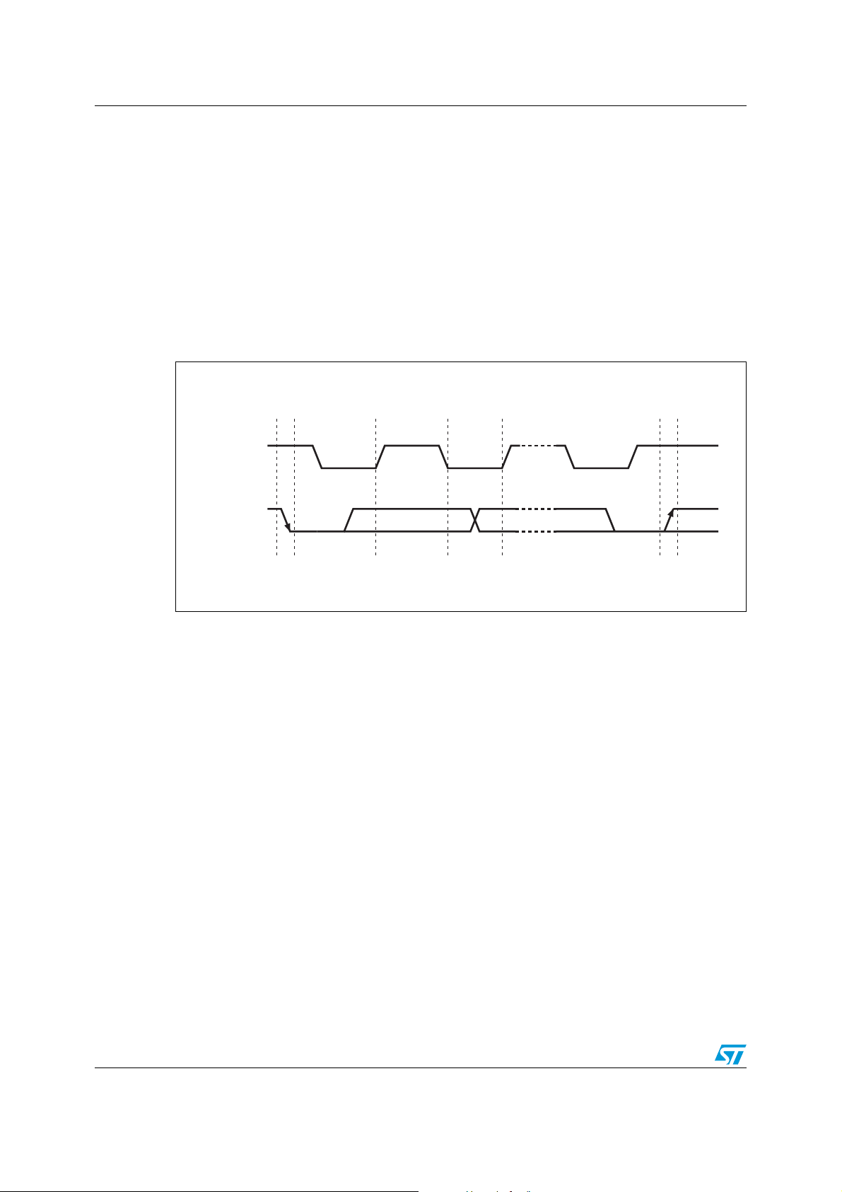
Accordingly, the following bus conditions have been defined (see Figure 6 on page 22):
3.4.1 Bus not busy
Both data and clock lines remain high.
3.4.2 Start data transfer
A change in the state of the data line, from high to low, while the clock is high, defines the
START condition.
3.4.3 Stop data transfer
A change in the state of the data line, from low to high, while the clock is high, defines the
STOP condition.
Doc ID 13298 Rev 11 21/41
Page 22
Functional description STTS75
3.4.4 Data valid
The state of the data line represents valid data when after a start condition, the data line is
stable for the duration of the high period of the clock signal. The data on the line may be
changed during the low period of the clock signal. There is one clock pulse per bit of data.
Each data transfer is initiated with a start condition and terminated with a stop condition.
The number of data bytes transferred between the start and stop conditions is not limited.
The information is transmitted byte-wide and each receiver acknowledges with a ninth bit.
By definition a device that gives out a message is called “transmitter,” the receiving device
that gets the message is called “receiver.” The device that controls the message is called
“master.” The devices that are controlled by the master are called “slaves.”
Figure 6. Serial bus data transfer sequence
DATA LINE
STABLE
DATA VALID
CLOCK
DATA
STA RT
CONDITION
CHANGE OF
DATA ALLOWED
STOP
CONDITION
AI00587
22/41 Doc ID 13298 Rev 11
Page 23
STTS75 Functional description
3.4.5 Acknowledge
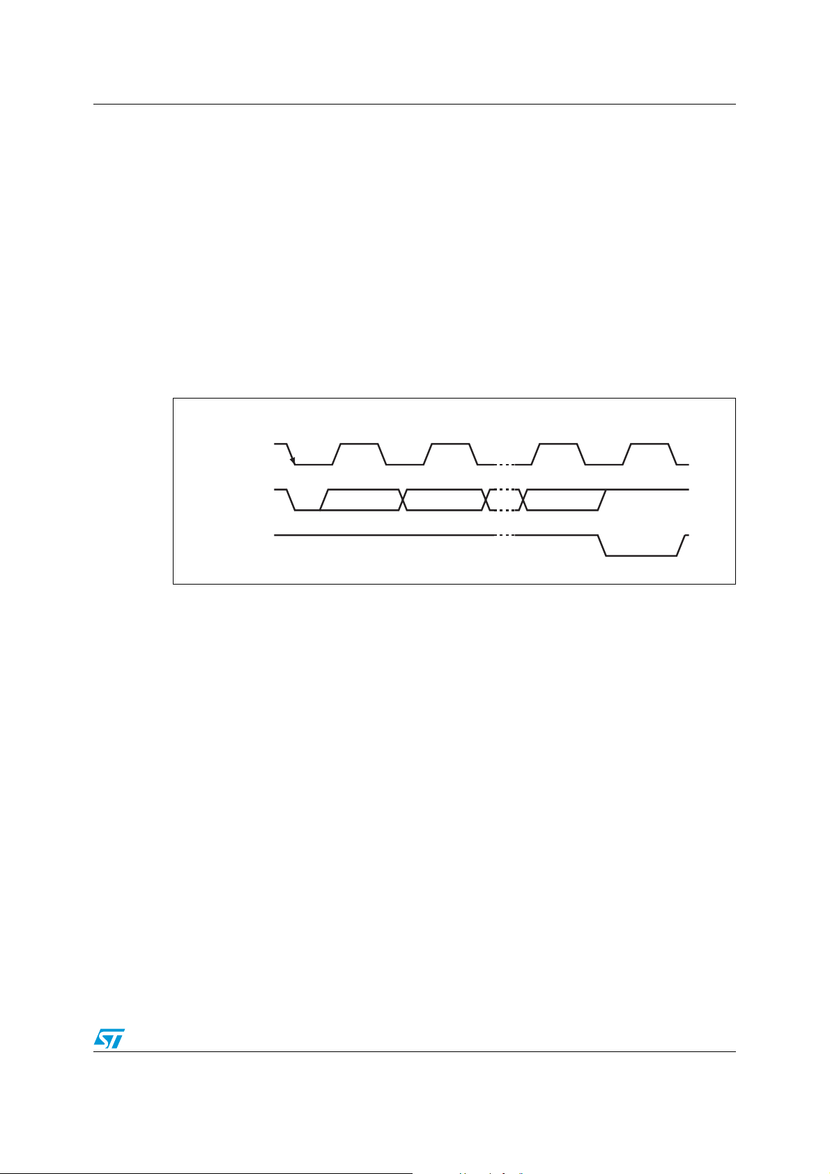
Each byte of eight bits is followed by one acknowledge bit. This acknowledge bit is a low
level put on the bus by the receiver whereas the master generates an extra acknowledge
related clock pulse (see Figure 7 on page 23). A slave receiver which is addressed is
obliged to generate an acknowledge after the reception of each byte that has been clocked
out of the slave transmitter.
The device that acknowledges has to pull down the SDA line during the acknowledge clock
pulse in such a way that the SDA line is a stable low during the high period of the
acknowledge related clock pulse. Of course, setup and hold times must be taken into
account. A master receiver must signal an end of data to the slave transmitter by not
generating an acknowledge on the last byte that has been clocked out of the slave. In this
case the transmitter must leave the data line high to enable the master to generate the
STOP condition.
Figure 7. Acknowledgement sequence
CLOCK PULSE FOR
ACKNOWLEDGEMENT
SCL FROM
MASTER
START
12 89
DATA OUTPUT
BY TRANSMITTER
DATA OUTPUT
BY RECEIVER
MSB LSB
AI00601
Doc ID 13298 Rev 11 23/41
Page 24
Functional description STTS75
3.5 READ mode
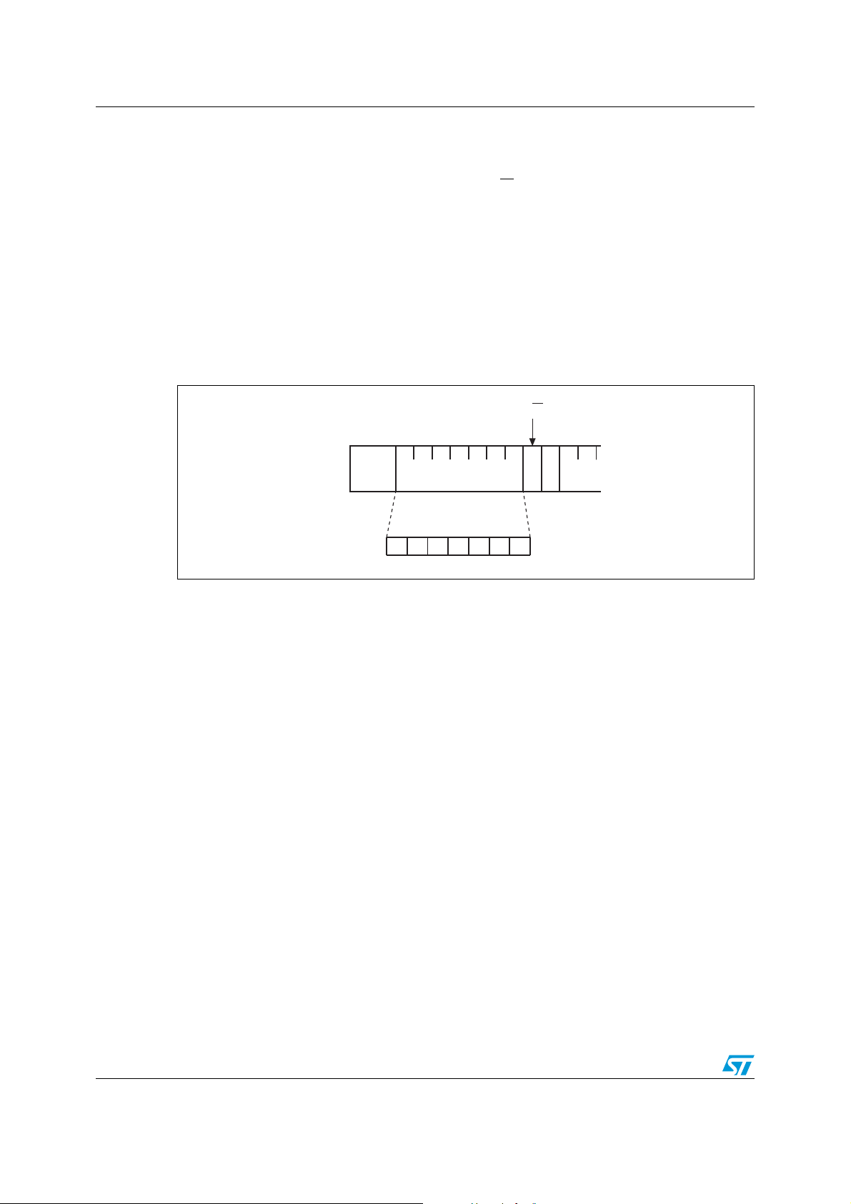
In this mode the master reads the STTS75 slave after setting the slave address (see
Figure 8). Following the WRITE mode control bit (R/W
address 'An' is written to the on-chip address pointer.
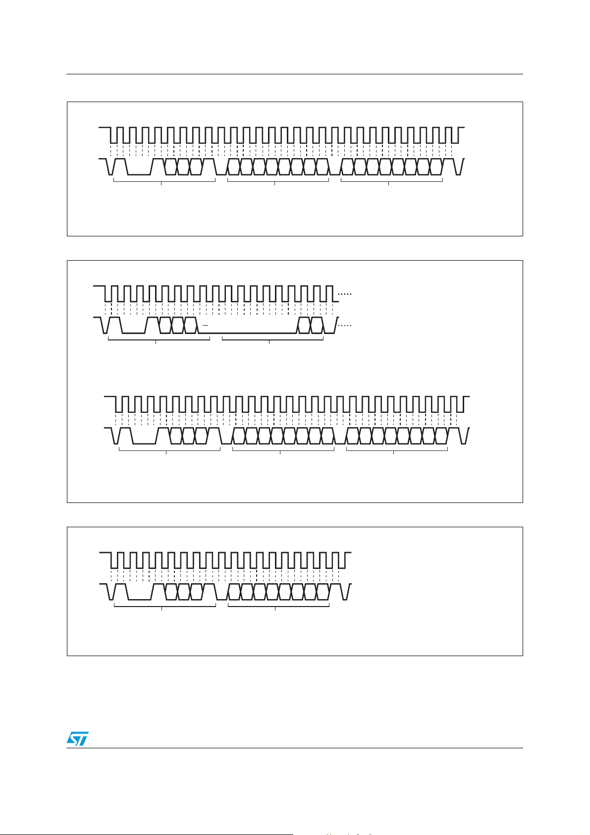
There are two READ modes:
● Preset pointer locations (e.g. Temperature, T
● Pointer setting (the pointer has to be set for the register that is to be read)
Note: The temperature register pointer is usually the default pointer.
These modes are shown in the READ mode typical timing diagrams (see Figure 9,
Figure 10, and Figure 11 on page 25).
Figure 8. Slave address location
=0) and the acknowledge bit, the word
OS
and T
R/W
registers), and
HYS
START A
SLAVE ADDRESS
MSB
0 1 A2 A1 A010
LSB
AI12226
24/41 Doc ID 13298 Rev 11
Page 25
STTS75 Functional description
Figure 9. Typical 2-byte READ from preset pointer location (e.g. temp - TOS, T
119199
1
0 0 1 A2 A1 A0 R D7 D6 D5 D4 D3 D2 D1 D0 D7 D6 D5 D4 D3 D2 D1 D0
Start
by
Master
Address Byte
Most Significant Data Byte Least Significant Data Byte
ACK
by
STTS75
ACK
by
Master
HYS
No ACK
by
Master
)
Stop
Cond.
by
Master
AI12281b
Figure 10. Typical pointer set followed by an immediate READ for 2-byte register (e.g. temp)
1199
1
0 0 1 A2 A1 A0 W 0 0 0 0 0 0 D1 D0
Start
by
Master
Address Byte
ACK
by
STTS75
Pointer Byte
ACK
by
STTS75
119199
0 0 1 A2 A1 A0 R D7 D6 D5 D4 D3 D2 D1 D0 D7 D6 D5 D4 D3 D2 D1 D0
1
Repeat
Start
by
Master
Address Byte
Most Significant Data Byte Least Significant Data Byte
ACK
by
STTS75
ACK
by
Master
No ACK
Master
Figure 11. Typical 1-byte READ from the configuration register with preset pointer
1199
1
0 0 1 A2 A1 A0 R D7 D6 D5 D4 D3 D2 D1 D0
Stop
Start
by
Master
Address Byte
ACK
by
STTS75
Data Byte
No ACK
Master
Cond.
by
Master
by
Stop
Cond.
by
Master
by
AI12282b
83b
AI122
Doc ID 13298 Rev 11 25/41
Page 26
Functional description STTS75
3.6 WRITE mode
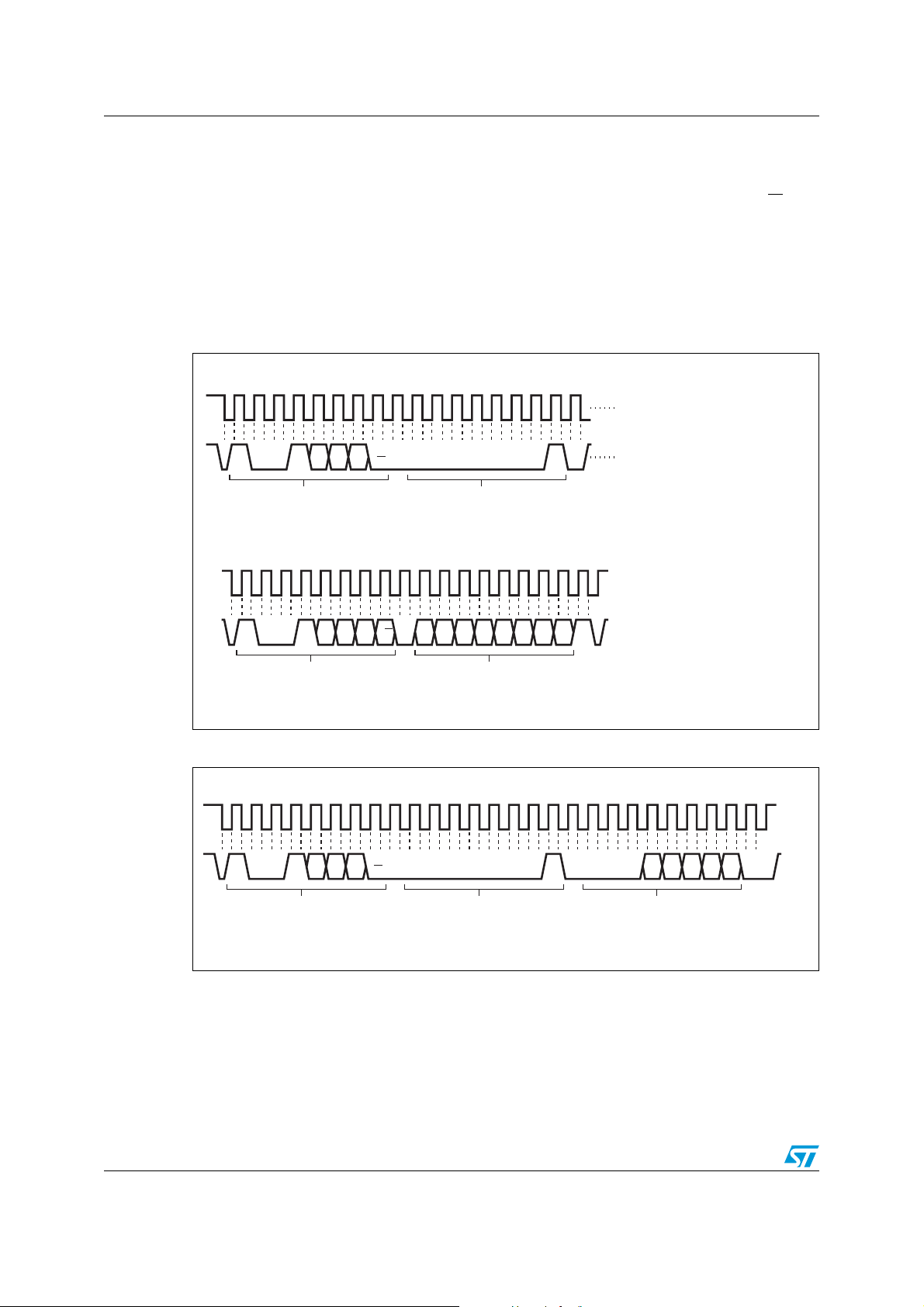
In this mode the master transmitter transmits to the STTS75 slave receiver. Bus protocol is
shown in Figure 12. Following the START condition and slave address, a logic '0' (R/W
is placed on the bus and indicates to the addressed device that word address will follow and
is to be written to the on-chip address pointer.
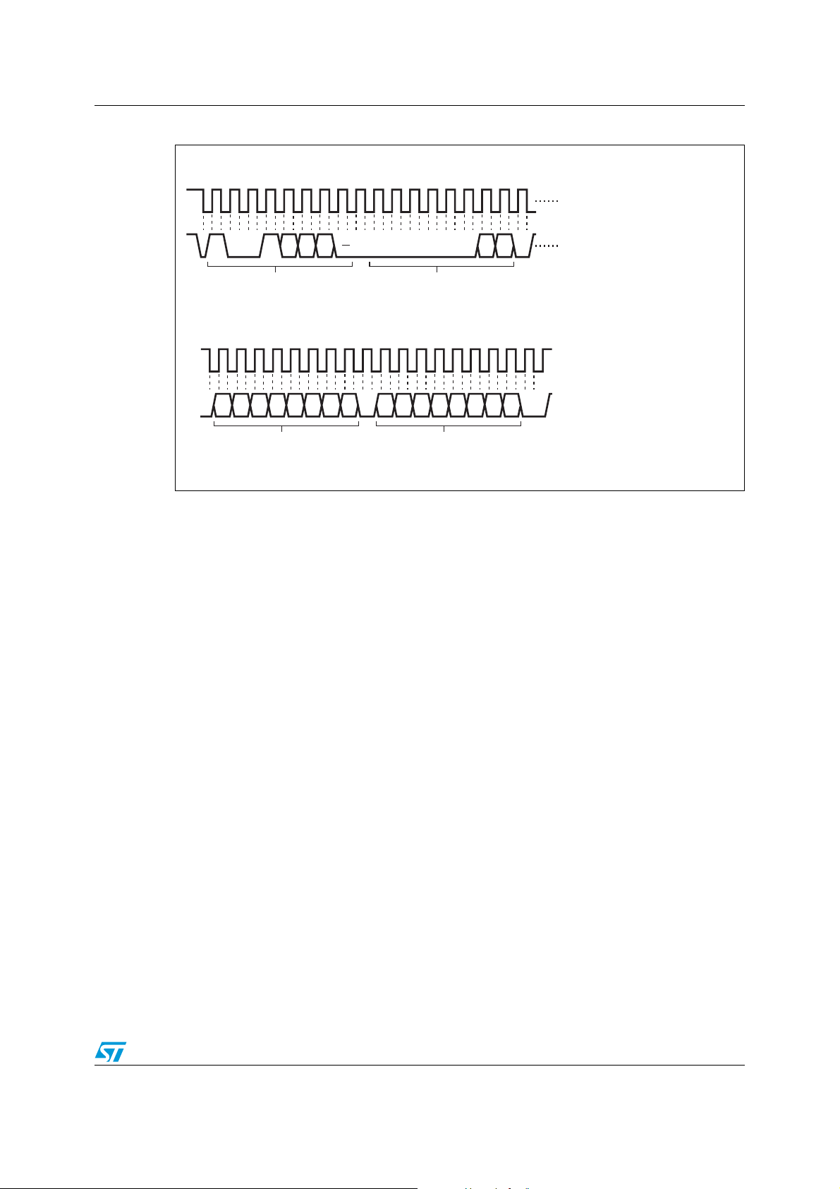
These modes are shown in the WRITE mode typical timing diagrams (see Figure 12, and
Figure 13, and Figure 14 on page 27).
Figure 12. Typical pointer set followed by an immediate READ from the
configuration register
1199
1
0 0 1 A2 A1 A0 W 0 0 0 0 0 0 D1 D0
= 0)
Start
by
Master
Repeat
Start
by
Master
Address Byte
1919
1 0 0 1 A2 A1 A0 D7 D6 D5 D4 D3 D2 D1 D0
Address Byte Data Byte
ACK
by
STTS75
R/W
ACK
by
STTS75
Pointer Byte
ACK
by
STTS75
No ACK
by
STTS75
Stop
Cond.
by
Master
AI12279b
Figure 13. Configuration register WRITE
119919
1
001A2A1A0W 000000 000D4D3 D2 D1 D0D1 D0
Start
by
Master
Address Byte
ACK
by
STTS75
Pointer Byte
ACK
by
STTS75
Configuration Byte
STTS75
ACK
by
Stop
Cond.
by
Master
AI12280b
26/41 Doc ID 13298 Rev 11
Page 27
STTS75 Functional description
Figure 14. TOS and T
1199
1
0 0 1 A2 A1 A0 W 0 0 0 0 0 0 D1 D0
Start
by
Master
Address Byte
1919
D7 D6 D5 D4 D3 D2 D1 D0 D7 D6 D5 D4 D3 D2 D1 D0
Most Significant Data Byte Least Significant Data Byte
HYS
WRITE
ACK
by
STTS75
ACK
by
STTS75
Pointer Byte
ACK
by
STTS75
ACK
by
STTS75
Stop
Cond.
by
Master
AI12284b
Doc ID 13298 Rev 11 27/41
Page 28
Typical operating characteristics STTS75
4 Typical operating characteristics
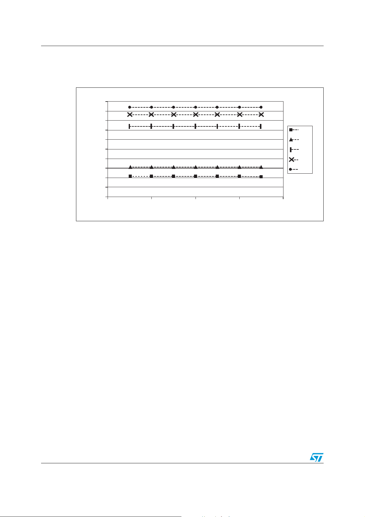
Figure 15. Temperature variation vs. voltage
140
120
100
80
60
40
20
0
Temperature (°C)
–20
–40
–60
23456
Voltage (V)
–20
0.5
85
110
125
AI12258
28/41 Doc ID 13298 Rev 11
Page 29
STTS75 Maximum ratings
5 Maximum ratings
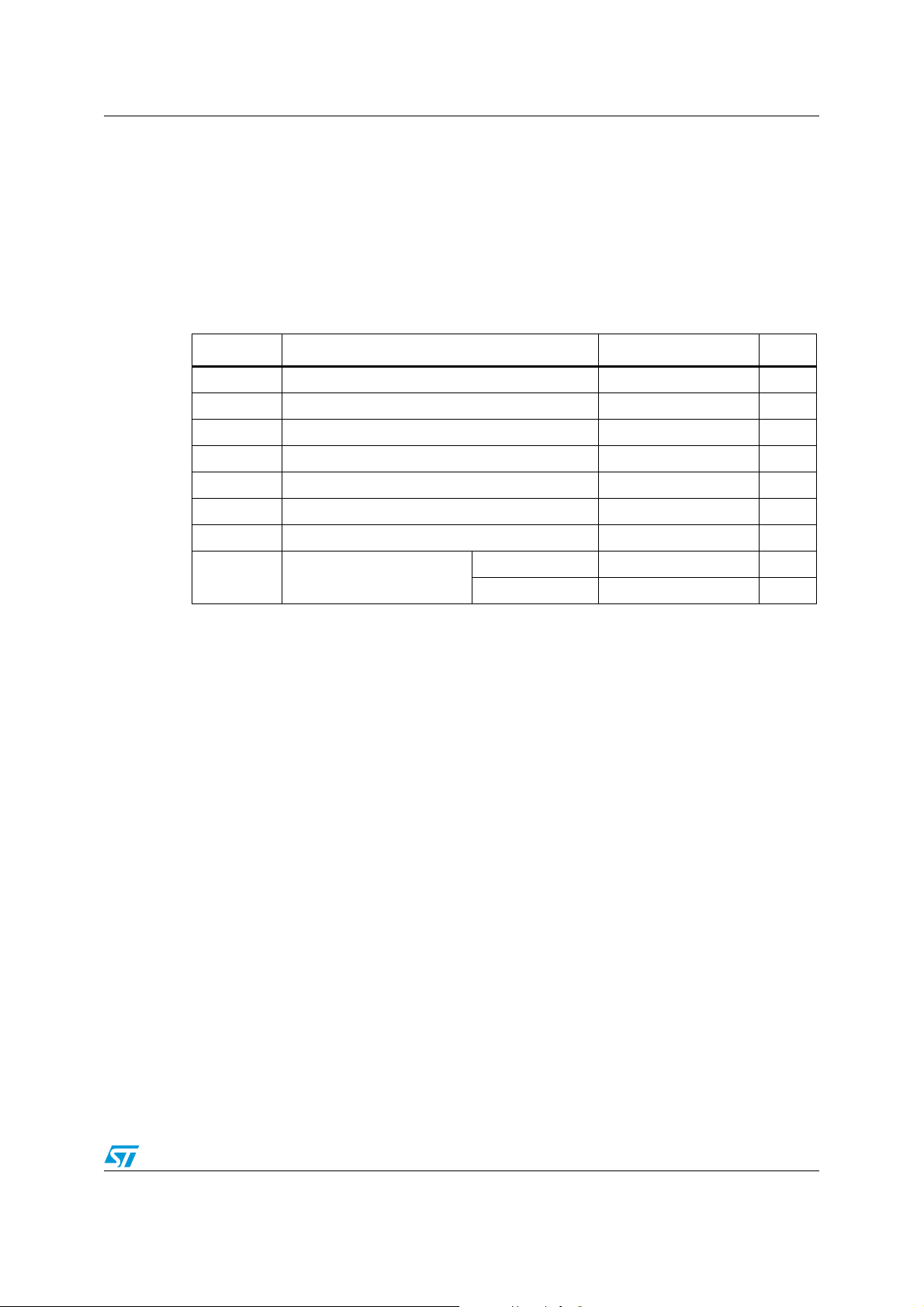
Stressing the device above the rating listed in the absolute maximum ratings table may
cause permanent damage to the device. These are stress ratings only and operation of the
device at these or any other conditions above those indicated in the operating sections of
this specification is not implied. Exposure to absolute maximum rating conditions for
extended periods may affect device reliability.
Table 12. Absolute maximum ratings
Symbol Parameter Value Unit
T
STG
T
SLD
V
IO
V
DD
V
OUT
I
O
P
D
Storage temperature –60 to 150 °C
(1)
Lead solder temperature for 10 seconds 260 °C
Input or output voltage VDD +0.5 V
Supply voltage 7.0 V
Output voltage VDD + 0.5 V
Output current 10 mA
Power dissipation 320 mW
SO8 128.4 °C/W
θ
JA
1. Reflow at peak temperature of 260 °C. The time above 255 °C must not exceed 30 seconds.
Thermal resistance
MSOP8 (TSSOP8) 216.3 °C/W
Doc ID 13298 Rev 11 29/41
Page 30
DC and AC parameters STTS75
6 DC and AC parameters
This section summarizes the operating measurement conditions, and the DC and AC
characteristics of the device. The parameters in the DC and AC characteristics tables that
follow, are derived from tests performed under the measurement conditions summarized in
Ta bl e 1 3. Designers should check that the operating conditions in their circuit match the
operating conditions when relying on the quoted parameters.
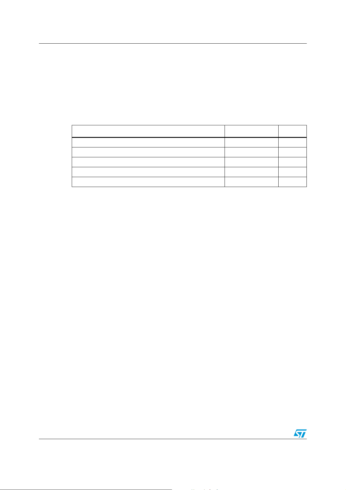
Table 13. Operating and AC measurement conditions
Parameter STTS75 Unit
Supply voltage 2.7 to 5.5 V
Ambient operating temperature (TA) –55 to 125 °C
Input rise and fall times ≤ 5ns
Input pulse voltages 0.2 to 0.8V
Input and output timing reference voltages 0.3 to 0.7V
DD
DD
V
V
30/41 Doc ID 13298 Rev 11
Page 31
STTS75 DC and AC parameters
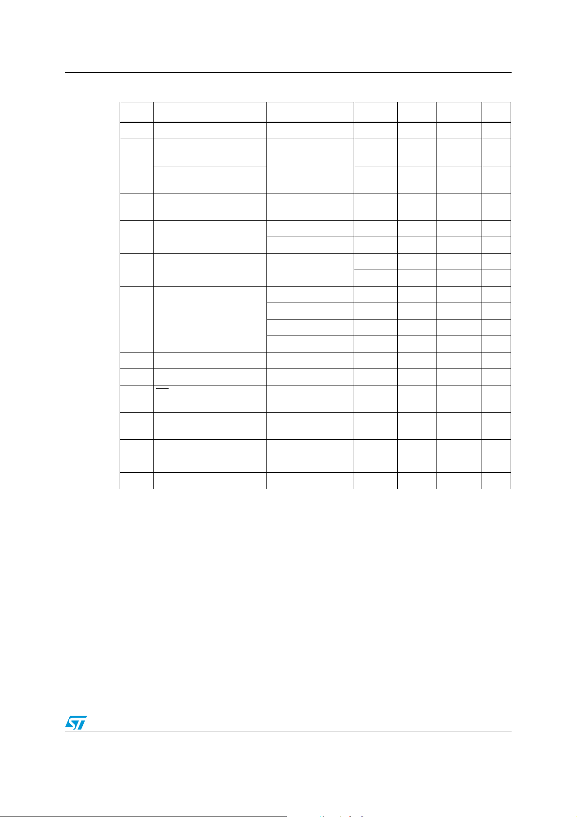
Table 14. DC and AC characteristics
Sym Description Test condition
V
Supply voltage TA = –55 to +125 °C 2.7 5.5 V
DD
VDD supply current, active
temperature conversions
I
DD
VDD supply current,
communication only
Standby supply current,
I
DD1
serial port inactive
Accuracy for corresponding
range 2.7 V ≤ V
Resolution
≤ 5.5 V
DD
V
= 3.3 V 75 100 µA
DD
= 25 °C 100 µA
T
A
= 25 °C 1.0 µA
T
A
–25 °C < T
–55 °C < T
< 100 ±0.5 ±2.0 °C
A
< 125 ±0.5 ±3.0 °C
A
9 to 12-bit
temperature data
94585ms
(1)
Min Typ
0.5 0.0625 °C
912bits
(2)
Max Unit
10 90 170 ms
CONV
Conversion time
11 180 340 ms
t
12 360 680 ms
T
Overtemperature shutdown Default value 80 °C
OS
T
V
V
1. Valid for ambient operating temperature: TA = –55 to 125 °C; VDD = 2.7 V to 5.5 V (except where noted).
2. Typical number taken at VDD = 3.0 V, TA = 25 °C
Hysteresis Default value 75 °C
HYS
OS/INT saturation voltage
OL1
(VDD = 5 V)
V
Input logic high
IH
V
Input logic low Digital pins –0.45 0.3 x V
IL
Output logic low (SDA) I
OL2
C
Capacitance 5 pF
IN
4 mA sink current 0.5 V
Digital pins (SCL,
SDA, A2-A0)
= 3 mA 0.4 V
OL2
0.7 x V
DD
VDD + 0.5 V
DD
V
Doc ID 13298 Rev 11 31/41
Page 32
DC and AC parameters STTS75
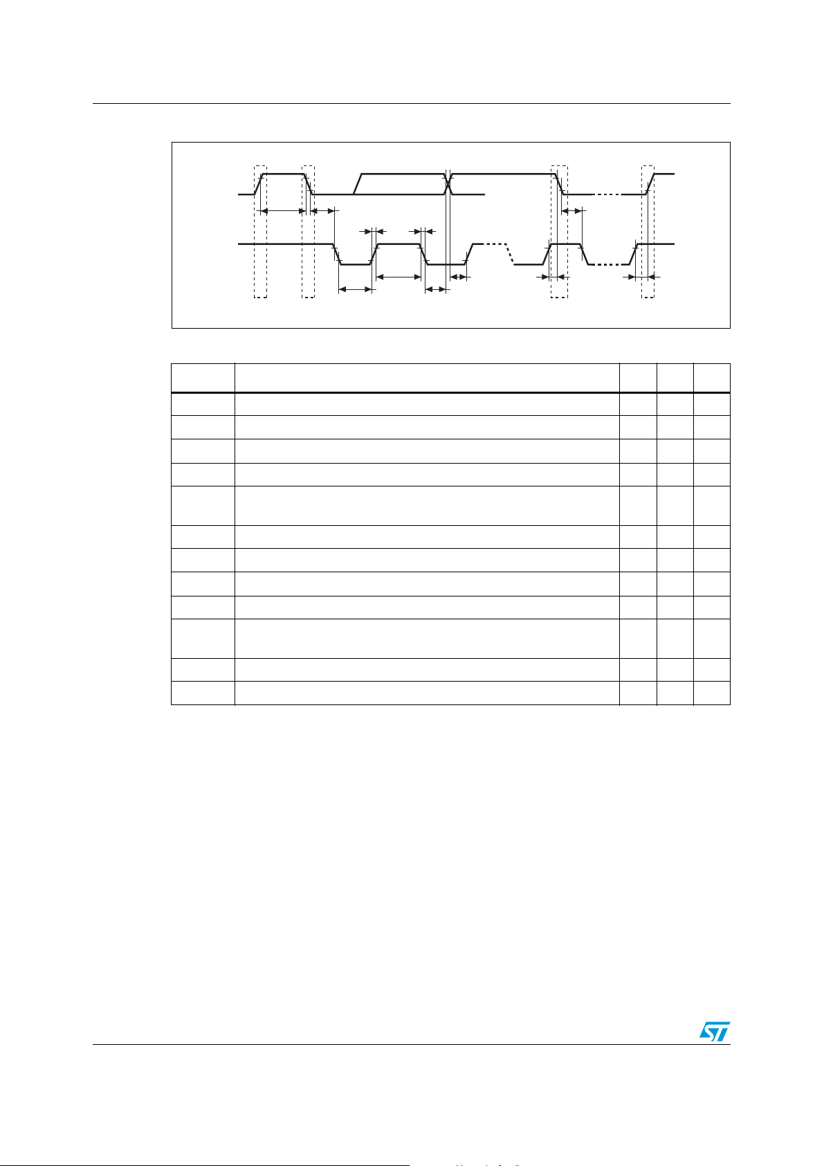
Figure 16. Bus timing requirements sequence
SDA
SR
t
SU:STA
t
HD:STA
Min Max Unit
600 ns
600 ns
75 325 ns
t
SU:STO
P
AI00589
t
BUF
SCL
Table 15. AC characteristics
t
HD:STA
t
t
LOW
t
HIGH
t
R
SP
Sym Parameter
f
SCL
t
BUF
t
HD:DAT
t
HD:STA
t
HIGH
t
LOW
t
SU:DAT
t
SU:STA
t
SU:STO
t
TIMEOUT
SCL clock frequency 0 400 kHz
Time the bus must be free before a new transmission can start 1.3 µs
t
SDA and SCL fall time 300 ns
F
(3)
Data hold time 0.9 µs
START condition hold time
(after this period the first clock pulse is generated)
Clock high period 600 ns
Clock low period 1.3 µs
t
SDA and SCL rise time 300 ns
R
Data setup time 100 ns
START condition setup time
(only relevant for a repeated start condition)
STOP condition setup time 600 ns
SDA low time for reset of serial interface
F
t
SU:DAT
t
HD:DAT
(1)(2)
(4)
1. Valid for ambient operating temperature: TA = –55 to 125 °C; VDD = 2.7 V to 5.5 V (except where noted).
2. Devices are tested at maximum clock frequency of 400 kHz.
3. Transmitter must internally provide a hold time to bridge the undefined region (300 ns max) of the falling
edge of SCL.
4. For SMBus compatibility STTS75 supports bus timeout. Holding the SDA line low for a period greater than
timeout duration will cause STTS75 to reset the SDA line to the state of serial bus communication (SDA
high).
32/41 Doc ID 13298 Rev 11
Page 33

STTS75 Package mechanical data
7 Package mechanical data
In order to meet environmental requirements, ST offers these devices in different grades of
ECOPACK
specifications, grade definitions and product status are available at: www.st.com.
ECOPACK
®
packages, depending on their level of environmental compliance. ECOPACK®
®
is an ST trademark.
Doc ID 13298 Rev 11 33/41
Page 34
Package mechanical data STTS75
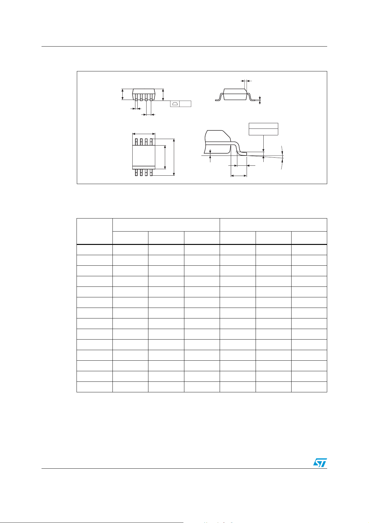
Figure 17. SO8 – 8-lead plastic small outline (4.90 mm x 3.90 mm) package
mechanical drawing
h x 45˚
A2
b
8
1
Note: Drawing is not to scale.
Table 16. SO8 – 8-lead plastic small outline (4.90 mm x 3.90 mm) package mechanical
data
Sym
Typ Min Max Typ Min Max
A1.750.069
A1 0.10 0.25 0.004 0.010
A2 1.25 0.049
A
ccc
e
D
E1
E
A1
L
L1
c
0.25 mm
GAUGE PLANE
k
SO-A
mm inches
b 0.28 0.48 0.011 0.019
c 0.17 0.23 0.007 0.009
ccc 0.10 0.004
D 4.90 4.80 5.00 0.193 0.189 0.197
E 6.00 5.80 6.20 0.236 0.228 0.244
E1 3.90 3.80 4.00 0.154 0.150 0.157
e1.27– –0.050– –
h 0.25 0.50 0.010 0.020
k 0°8° 0°8°
L 0.40 1.27 0.016 0.050
L1 1.04 0.041
34/41 Doc ID 13298 Rev 11
Page 35
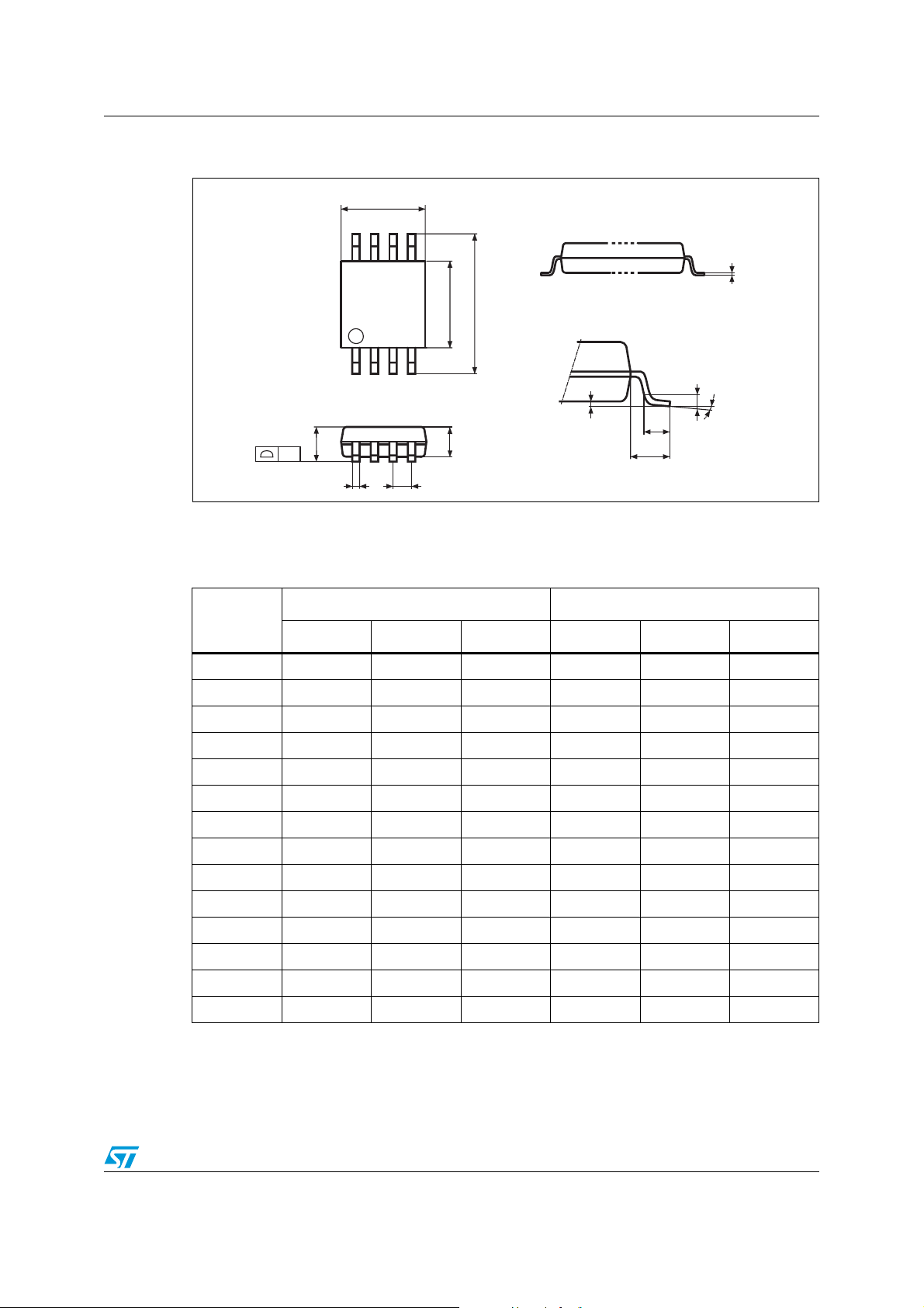
STTS75 Package mechanical data
Figure 18. MSOP8 (TSSOP8) – 8-lead, thin shrink small outline (3 mm x 3 mm) package
mechanical drawing
D
ccc
Note: Drawing is not to scale.
Table 17. MSOP8 (TSSOP8) – 8-lead, thin shrink small outline (3 mm x 3 mm) package
mechanical data
Sym
Typ Min Max Typ Min Max
A1.100.043
A1 0.00 0.15 0.000 0.006
A2 0.85 0.75 0.95 0.034 0.030 0.037
b 0.22 0.40 0.009 0.016
8
1
5
EE1
4
A2A
A1
eb
L
L1
c
k
L2
E3_ME
mm inches
c 0.08 0.23 0.003 0.009
D 3.00 2.80 3.20 0.118 0.110 0.126
E 4.90 4.65 5.15 0.193 0.183 0.203
E1 3.00 2.80 3.10 0.118 0.110 0.122
e0.65 0.026
L 0.60 0.40 0.80 0.024 0.016 0.032
L1 0.95 0.037
L2 0.25 0.010
k 0°8° 0°8°
ccc 0.10 0.004
Doc ID 13298 Rev 11 35/41
Page 36
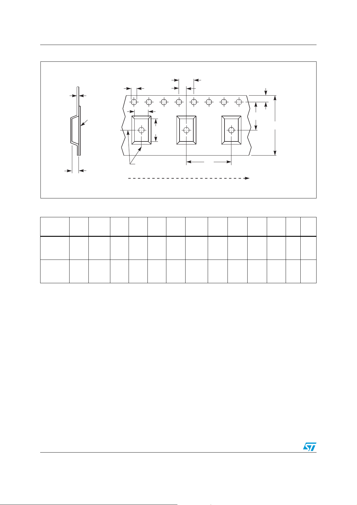
Package mechanical data STTS75
Figure 19. Carrier tape for SO8 and MSOP8 (TSSOP8) packages
P
D
T
A
TOP COVER
TAPE
K
0
0
CENTER LINES
OF CAVITY
P
2
B
0
0
P
1
E
F
W
USER DIRECTION OF FEED
Table 18. Carrier tape dimensions for SO8 and MSOP8 (TSSOP8) packages
Package W D E P
1.50
+0.10/
–0.00
1.50
+0.10/
–0.00
1.75
±0.10
1.75
±0.10
SO8
MSOP8
(TSSOP8)
12.00
±0.30
12.00
±0.30
4.00
±0.10
4.00
±0.10
P
0
2.00
±0.10
2.00
±0.10
FA0B
2
5.50
±0.05
5.50
±0.05
6.50
±0.10
5.30
±0.10
0
5.30
±0.10
3.40
±0.10
K
0
2.20
±0.10
1.40
±0.10
P
8.00
±0.10
8.00
±0.10
1
AM03073v1
TUnit
0.30
0.30
mm 2500
mm 4000
±0.05
±0.05
Bulk
Qty
36/41 Doc ID 13298 Rev 11
Page 37
STTS75 Package mechanical data
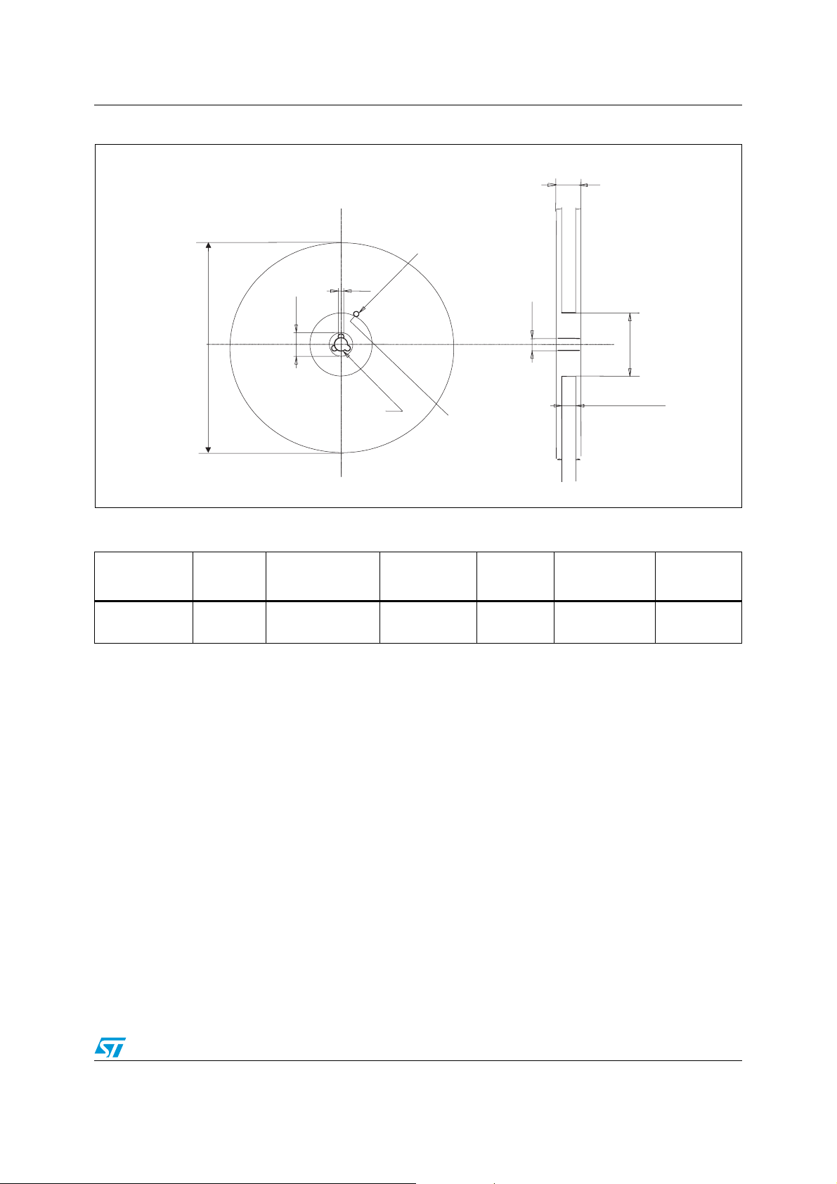
Figure 20. Reel schematic
T
40mm min.
Access hole
At slot location
B
D
C
A
Tape slot
Full ra dius
In core for
Tape s tart
2.5mm min.width
N
G measured
At hub
AM04928v1
Table 19. Reel dimensions for 12 mm carrier tape - SO8 and MSOP8 (TSSOP8) packages
A
(max)
330 mm
(13-inch)
B
(min)
1.5 mm
C
13 mm
± 0.2 mm
D
(min)
N
(min)
20.2 mm 60 mm
G
12.4 mm
+ 2/–0 mm
T
(max)
18.4 mm
Note: The dimensions given in Tab le 1 9 incorporate tolerances that cover all variations on critical
parameters.
Doc ID 13298 Rev 11 37/41
Page 38

Part numbering STTS75
8 Part numbering
Table 20. Ordering information scheme
Example: STTS75 M 2 F
Device type
STTS75
Package
M = SO8
DS = MSOP8 (TSSOP8)
Temperature range
2 = –55 to 125 °C
Shipping method
F = ECOPACK® package, tape & reel
®
E = ECOPACK
package, tube
For other options, or for more information on any aspect of this device, please contact the
ST sales office nearest you.
38/41 Doc ID 13298 Rev 11
Page 39
STTS75 Package marking information
9 Package marking information
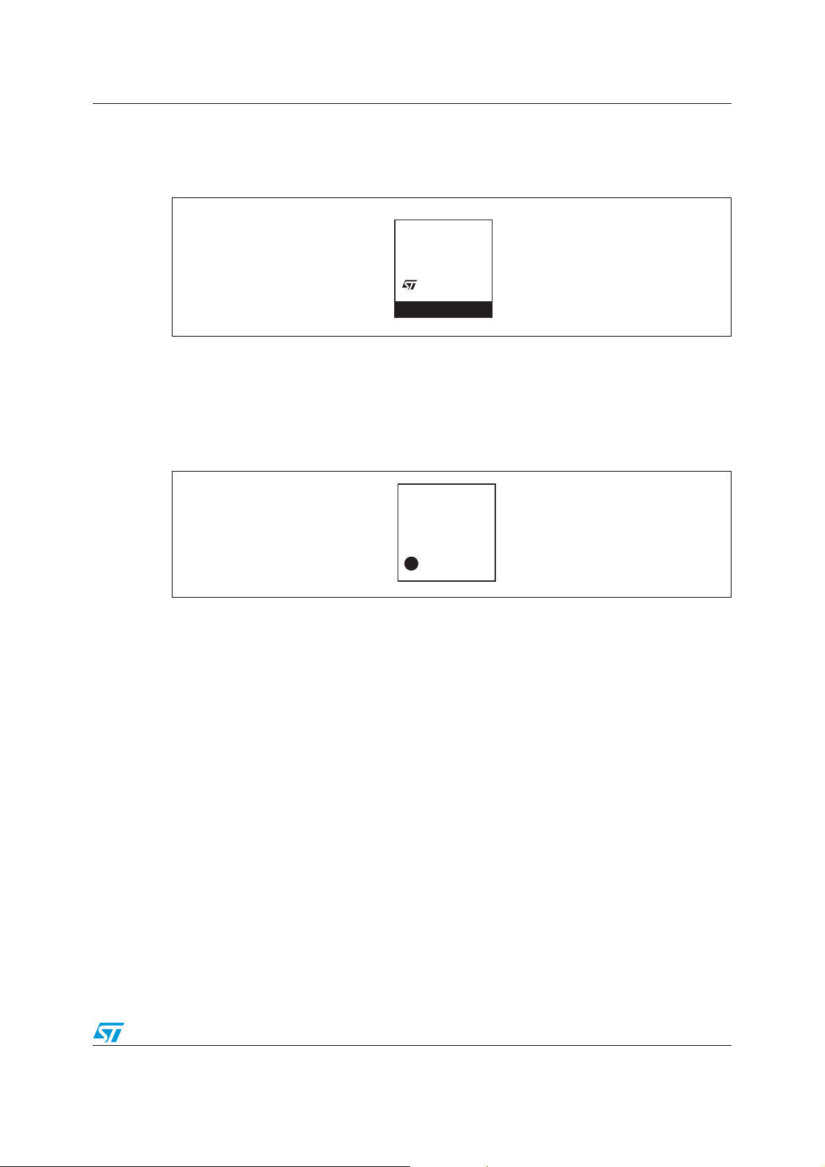
Figure 21. Device topside marking information (SO8)
STTS75M2
(1
EPYWW
1. Traceability codes
E = Additional information
P = Plant code
Y = Year
WW = Work Week
Figure 22. Device topside marking information (MSOP8/TSSOP8)
)
ai13912
1. Traceability codes
P = Plant code
Y = Year
WW = Work Week
TS75
PYWW
(1
)
ai13913
Doc ID 13298 Rev 11 39/41
Page 40
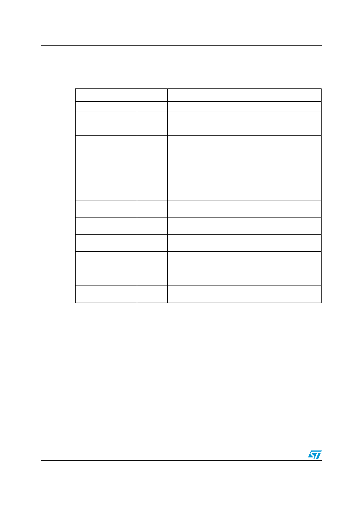
Revision history STTS75
10 Revision history
Table 21. Document revision history
Date Revision Changes
14-Jun-2006 1 Initial release.
Update features (cover page), DC and AC characteristics
22-Jan-2007 2
01-Mar-2007 3
18-Apr-2007 4
09-May-2007 5 Updated cover page, Figure 19, 22, Ta bl e 1 4, and 20.
(Ta bl e 14 ), package mecanical information (Figure 17,
Ta bl e 1 6 , Figure 18, Ta bl e 1 7 ) and part numbering (Ta bl e 2 0 ).
Update cover page (package information); Section 2:
Operation; Section 2.3: Comparator mode; Section 2.8: Bus
timeout feature; Ta bl e 1 4 ; package mechanical data
(Figure 18 and Ta bl e 1 7 ); and part numbering (Ta bl e 2 0 ).
Package information (DFN8) added to cover page, Figure 2,
Figure 19, Table 18. AddedSection 9: Package marking
information. Updated Ta b le 1 2 , 13, 15, and 18.
16-May-2007 6
06-Jun-2007 7
07-Jul-2008 8
18-Jul-2008 9 Updated cover page and Ta b le 2 0 .
09-Apr-2009 10
15-Jun-2010 11
Updated cover page, Figure 4, Section 3.1.3, Section 3.1.5,
Ta bl e 8 , 14, and 15.
Updated cover page, document status upgraded to full
datasheet, updated Figure 2, Section 7, 8, 9.
Minor text changes; added Section 2.9: One-shot mode;
updated Section 3.1.3: Temperature register.
Updated Features, Ta bl e 1 2 , 14, 15, text in Section 7:
Package mechanical data; added tape and reel information
Figure 19, Ta b le 1 8 ; minor reformatting.
Updated Section 2.5, Section 5; added Figure 20, Ta bl e 1 9 ;
minor textual changes; reformatted document.
40/41 Doc ID 13298 Rev 11
Page 41

STTS75
Please Read Carefully:
Information in this document is provided solely in connection with ST products. STMicroelectronics NV and its subsidiaries (“ST”) reserve the
right to make changes, corrections, modifications or improvements, to this document, and the products and services described herein at any
time, without notice.
All ST products are sold pursuant to ST’s terms and conditions of sale.
Purchasers are solely responsible for the choice, selection and use of the ST products and services described herein, and ST assumes no
liability whatsoever relating to the choice, selection or use of the ST products and services described herein.
No license, express or implied, by estoppel or otherwise, to any intellectual property rights is granted under this document. If any part of this
document refers to any third party products or services it shall not be deemed a license grant by ST for the use of such third party products
or services, or any intellectual property contained therein or considered as a warranty covering the use in any manner whatsoever of such
third party products or services or any intellectual property contained therein.
UNLESS OTHERWISE SET FORTH IN ST’S TERMS AND CONDITIONS OF SALE ST DISCLAIMS ANY EXPRESS OR IMPLIED
WARRANTY WITH RESPECT TO THE USE AND/OR SALE OF ST PRODUCTS INCLUDING WITHOUT LIMITATION IMPLIED
WARRANTIES OF MERCHANTABILITY, FITNESS FOR A PARTICULAR PURPOSE (AND THEIR EQUIVALENTS UNDER THE LAWS
OF ANY JURISDICTION), OR INFRINGEMENT OF ANY PATENT, COPYRIGHT OR OTHER INTELLECTUAL PROPERTY RIGHT.
UNLESS EXPRESSLY APPROVED IN WRITING BY AN AUTHORIZED ST REPRESENTATIVE, ST PRODUCTS ARE NOT
RECOMMENDED, AUTHORIZED OR WARRANTED FOR USE IN MILITARY, AIR CRAFT, SPACE, LIFE SAVING, OR LIFE SUSTAINING
APPLICATIONS, NOR IN PRODUCTS OR SYSTEMS WHERE FAILURE OR MALFUNCTION MAY RESULT IN PERSONAL INJURY,
DEATH, OR SEVERE PROPERTY OR ENVIRONMENTAL DAMAGE. ST PRODUCTS WHICH ARE NOT SPECIFIED AS "AUTOMOTIVE
GRADE" MAY ONLY BE USED IN AUTOMOTIVE APPLICATIONS AT USER’S OWN RISK.
Resale of ST products with provisions different from the statements and/or technical features set forth in this document shall immediately void
any warranty granted by ST for the ST product or service described herein and shall not create or extend in any manner whatsoever, any
liability of ST.
ST and the ST logo are trademarks or registered trademarks of ST in various countries.
Information in this document supersedes and replaces all information previously supplied.
The ST logo is a registered trademark of STMicroelectronics. All other names are the property of their respective owners.
© 2010 STMicroelectronics - All rights reserved
STMicroelectronics group of companies
Australia - Belgium - Brazil - Canada - China - Czech Republic - Finland - France - Germany - Hong Kong - India - Israel - Italy - Japan -
Malaysia - Malta - Morocco - Philippines - Singapore - Spain - Sweden - Switzerland - United Kingdom - United States of America
www.st.com
Doc ID 13298 Rev 11 41/41
 Loading...