

Page 1
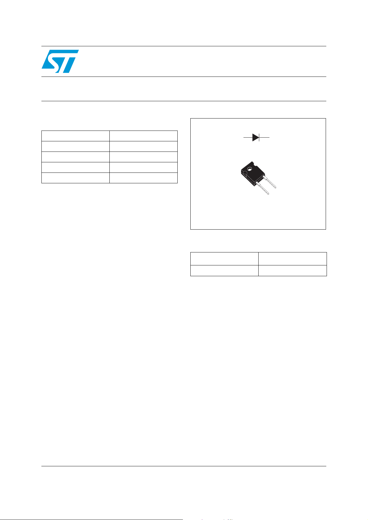
Main product characteristics
STTH6010
Ultrafast recovery - high voltage diode
I
F(AV)
V
RRM
T
j
V
(typ) 1.3 V
F
(typ) 49 ns
t
rr
60 A
1000 V
175° C
Features and benefits
■ Ultrafast, soft recovery
■ Very low conduction and switching losses
■ High frequency and/or high pulsed current
operation
■ High reverse voltage capability
■ High junction temperature
Description
The high quality design of this diode has
produced a device with low leakage current,
regularly reproducible characteristics and intrinsic
ruggedness. These characteristics make it ideal
for heavy duty applications that demand long term
reliability.
KA
A
K
DO-247
STTH6010W
Order codes
Part Number Marking
STTH6010W STTH6010W
Such demanding applications include industrial
power supplies, motor control, and similar
mission-critical systems that require rectification
and freewheeling. These diodes also fit into
auxiliary functions such as snubber, bootstrap,
and demagnetization applications.
The improved performance in low leakage
current, and therefore thermal runaway guard
band, is an immediate competitive advantage for
this device.
March 2006 Rev 1 1/8
www.st.com
8
Page 2
Characteristics STTH6010
1 Characteristics
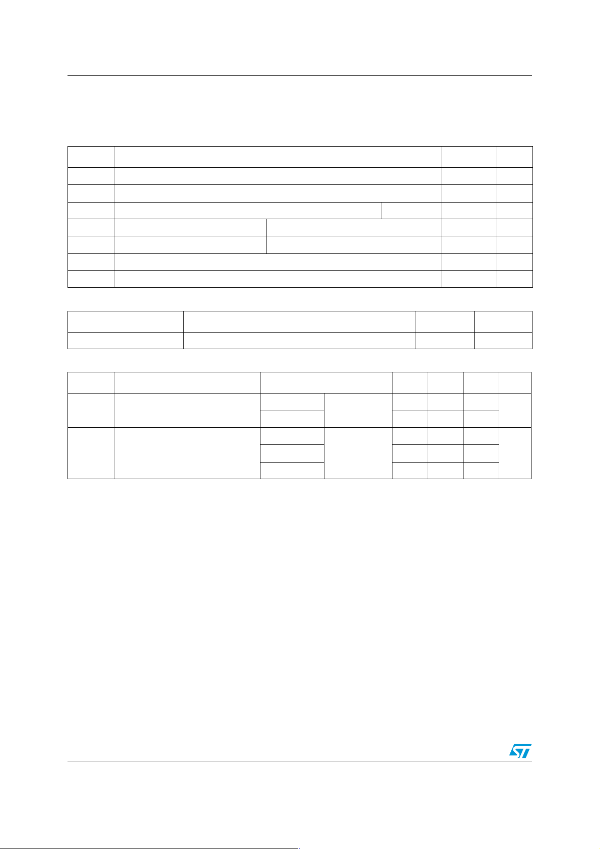
Table 1. Absolute ratings (limiting values at 25° C, unless otherwise specified)
Symbol Parameter Value Unit
V
RRM
I
F(RMS)
I
F(AV)
I
FRM
I
FSM
T
Table 2. Thermal parameters
Repetitive peak reverse voltage 1000 V
RMS forward current 80 A
Average forward current, δ = 0.5 Tc = 75° C 60 A
Repetitive peak forward current tp = 5 µs, F = 5 kHz square 450 A
Surge non repetitive forward current tp = 10 ms Sinusoidal 400 A
Storage temperature range -65 to + 175 °C
stg
T
Maximum operating junction temperature 175 °C
j
Symbol Parameter Value Unit
R
th(j-c)
Table 3. Static electrical characteristics
Junction to case 0.78 °C/W
Symbol Parameter Test conditions Min. Typ Max. Unit
T
= 25° C
(1)
I
R
Reverse leakage current
j
Tj = 125° C 20 200
= V
V
R
RRM
20
µA
(2)
V
1. Pulse test: tp = 5 ms, δ < 2 %
2. Pulse test: t
Forward voltage drop
F
= 380 µs, δ < 2 %
p
To evaluate the conduction losses use the following equation:
P = 1.3 x I
F(AV)
+ 0.0067 I
= 25° C
T
j
I
= 60 A
F
Tj = 150° C 1.3 1.7
F2(RMS)
2.0
VTj = 100° C 1.4 1.8
2/8
Page 3
STTH6010 Characteristics
Table 4. Dynamic characteristics
Symbol Parameter
t
Reverse recovery time
rr
I
Reverse recovery current
RM
S Softness factor
Forward recovery time
t
fr
V
Forward recovery voltage
FP
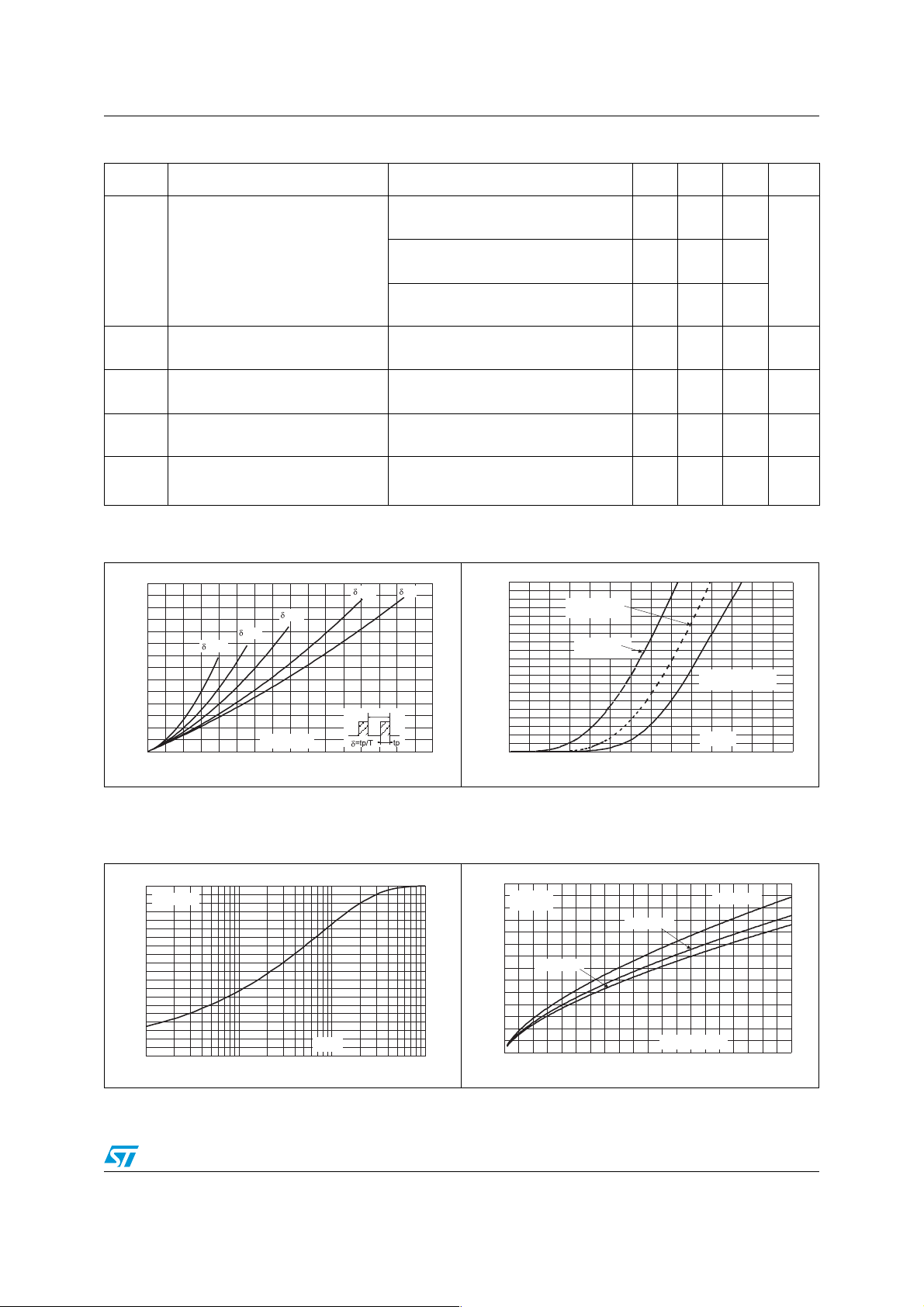
Figure 1. Conduction losses versus
average current
P(W)
140
120
100
80
60
40
20
0
0 1020304050607080
=0.05
=0.1
I(A)
F(AV)
=0.2
=0.5
Test conditions
IF = 1 A, dIF/dt = -50 A/µs,
V
= 30 V, Tj = 25° C
R
= 1 A, dIF/dt = -100 A/µs,
I
F
= 30 V, Tj = 25° C
V
R
IF = 1 A, dIF/dt = -200 A/µs,
= 30 V, Tj = 25° C
V
R
IF = 60 A, dIF/dt = -200 A/µs,
V
= 600 V, Tj = 125° C
R
= 60 A, dIF/dt = -200 A/µs,
I
F
= 600 V, Tj = 125° C
V
R
= 60 A dIF/dt = 100 A/µs
I
F
= 1.5 x V
V
FR
I
= 60 A, dIF/dt = 100 A/µs,
F
, Tj = 25° C
Fmax
Tj = 25° C
Figure 2. Forward voltage drop versus
I (A)
FM
=1
T
200
180
160
140
120
100
80
60
40
20
0
0.0 0.5 1.0 1.5 2.0 2.5 3.0 3.5
Min. Typ Max. Unit
forward current
Tj=150°C
(Maximum values)
Tj=150°C
(Typical values)
115
61 80
ns
49 65
31 40 A
1
750 ns
4V
Tj=25°C
(Maximum values)
V(V)
FM
Figure 3. Relative variation of thermal
impedance junction to case
versus pulse duration
Z/R
th(j-c) th(j-c)
1.0
Single pulse
0.9
0.8
0.7
0.6
0.5
0.4
0.3
0.2
0.1
0.0
1.E-03 1.E-02 1.E-01 1.E+00
t (s)
p
Figure 4. Peak reverse recovery current
versus dI
I (A)
RM
70
VR=600V
T
=125°C
j
60
50
40
30
20
10
3/8
IF=0.5 x I
F(AV)
0
0 50 100 150 200 250 300 350 400 450 500
/dt (typical values)
F
IF= 2 x I
IF= I
F(AV)
dI /dt(A/µs)
F
F(AV)
Page 4
Characteristics STTH6010
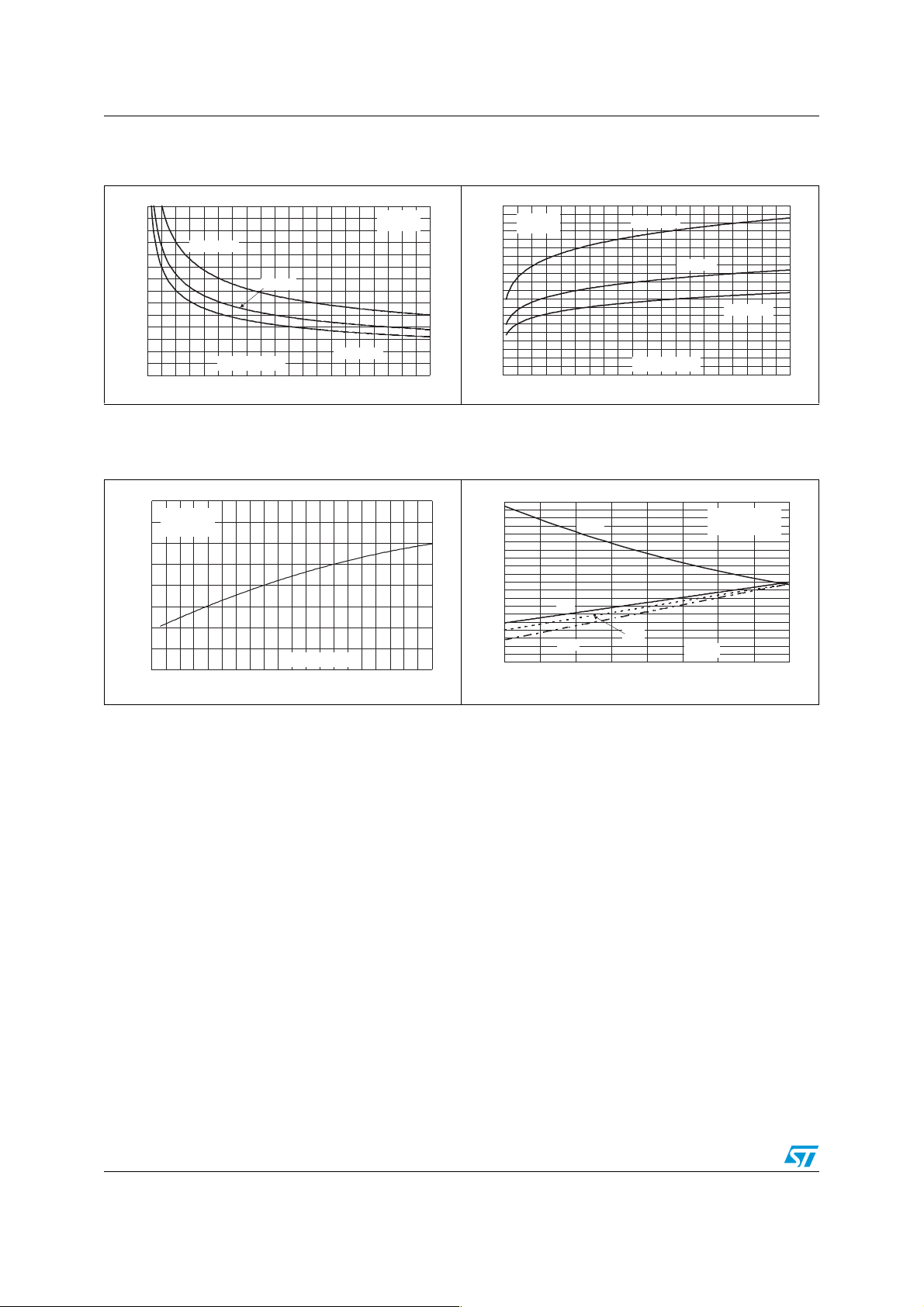
Figure 5. Reverse recovery time versus
dI
/dt (typical values)
F
t (ns)
rr
700
600
IF= 2 x I
F(AV)
dI /dt(A/µs)
F
IF=I
)
F(AV
500
400
300
200
100
0
0 50 100 150 200 250 300 350 400 450 500
IF=0.5 x I
VR=600V
T
=125°C
j
F(AV)
Figure 7. Softness factor versus
dI
/dt (typical values)
F
S factor
1.50
IF=2 x I
F(AV)
VR=600V
=125°C
T
1.25
1.00
0.75
0.50
j
dI /dt(A/µs)
F
0 50 100 150 200 250 300 350 400 450 500
Figure 6. Reverse recovery charges versus
dIF/dt (typical values)
Q (µC)
rr
10
VR=600V
9
T
=125°C
j
8
7
6
5
4
3
2
1
0
0 50 100 150 200 250 300 350 400 450 500
IF= 2 x I
F(AV)
dI /dt(A/µs)
F
IF= I
F(AV)
IF=0.5 x I
F(AV)
Figure 8. Relative variations of dynamic
parameters versus junction
temperature
2.0
1.8
1.6
1.4
1.2
1.0
0.8
0.6
0.4
0.2
0.0
25 50 75 100 125
S
factor
I
RM
t
Q
RR
RR
T (°C)
j
IF= I
VR=600V
Reference: T
F(AV)
=125°C
j
4/8
Page 5
STTH6010 Characteristics
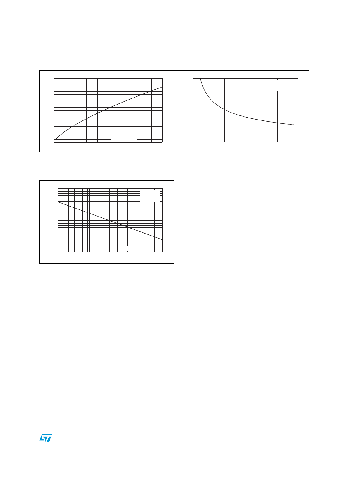
Figure 9. Transient peak forward voltage
versus dI
V(V)
FP
20
IF= I
F(AV)
18
Tj=125°C
16
14
12
10
8
6
4
2
0
0 100 200 300 400 500
/dt (typical values)
F
dI /dt(A/µs)
F
Figure 11. Junction capacitance versus
reverse voltage applied (typical
values)
C(pF)
1000
100
V
osc
F=1MHz
=30mV
Tj=25°C
Figure 10. Forward recovery time versus dI
F
/dt
(typical values)
t (ns)
fr
1200
1000
800
600
400
dI /dt(A/µs)
200
0 100 200 300 400 500
RMS
F
IF= I
F(AV)
VFR= 1.5 x VFmax.
=125°C
T
j
V(V)
10
1 10 100 1000
R
5/8
Page 6
Package information STTH6010
2 Package information
Epoxy meets UL94, V0
Cooling method: by conduction (C)
Recommended torque value: 0.80 Nm
Maximum torque value: 1.0 Nm
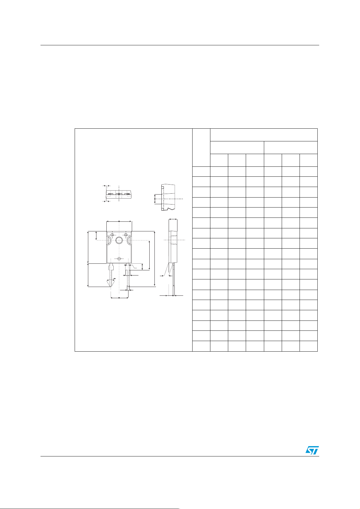
Table 5. DO-247 dimensions
DIMENSIONS
REF.
Millimeters Inches
Min. Max Min. Max.
A 4.85 5.15 0.191 0.203
V
D 2.20 2.60 0.086 0.102
E 0.40 0.80 0.015 0.031
V
H
L5
L
L3
V2
F
G
Dia
A
F 1.00 1.40 0.039 0.055
F2 2.00 0.078
F3 2.00 2.40 0.078 0.094
G 10.90 0.429
H 15.45 15.75 0.608 0.620
L2
L4
F2
L1
F3
D
L 19.85 20.15 0.781 0.793
L1 3.70 4.30 0.145 0.169
L2 18.50 0.728
L3 14.20 14.80 0.559 0.582
ME
L4 34.60 1.362
L5 5.50 0.216
M 2.00 3.00 0.078 0.118
V5° 5°
In order to meet environmental requirements, ST offers these devices in ECOPACK®
packages. These packages have a Lead-free second level interconnect . The category of
second level interconnect is marked on the package and on the inner box label, in
compliance with JEDEC Standard JESD97. The maximum ratings related to soldering
conditions are also marked on the inner box label. ECOPACK is an ST trademark.
ECOPACK specifications are available at: www.st.com.
6/8
V2 60° 60°
Dia. 3.55 3.65 0.139 0.143
Page 7
STTH6010 Ordering information
3 Ordering information
Part Number Marking Package Weight Base qty Delivery mode
STTH6010W STTH6010W DO-247
4 Revision history
Date Revision Description of Changes
02-Mar-2006 1 First issue.
4.4 g
30 Tube
7/8
Page 8

STTH6010
Please Read Carefully:
Information in this document is provided solely in connection with ST products. STMicroelectronics NV and its subsidiaries (“ST”) reserve the
right to make changes, corrections, modifications or improvements, to this document, and the products and services described herein at any
time, without notice.
All ST products are sold pursuant to ST’s terms and conditions of sale.
Purchasers are solely responsible for the choice, selection and use of the ST products and services described herein, and ST assumes no
liability whatsoever relating to the choice, selection or use of the ST products and services described herein.
No license, express or implied, by estoppel or otherwise, to any intellectual property rights is granted under this document. If any part of this
document refers to any third party products or services it shall not be deemed a license grant by ST for the use of such third party products
or services, or any intellectual property contained therein or considered as a warranty covering the use in any manner whatsoever of such
third party products or services or any intellectual property contained therein.
UNLESS OTHERWISE SET FORTH IN ST’S TERMS AND CONDITIONS OF SALE ST DISCLAIMS ANY EXPRESS OR IMPLIED
WARRANTY WITH RESPECT TO THE USE AND/OR SALE OF ST PRODUCTS INCLUDING WITHOUT LIMITATION IMPLIED
WARRANTIES OF MERCHANTABILITY, FITNESS FOR A PARTICULAR PURPOSE (AND THEIR EQUIVALENTS UNDER THE LAWS
OF ANY JURISDICTION), OR INFRINGEMENT OF ANY PATENT, COPYRIGHT OR OTHER INTELLECTUAL PROPERTY RIGHT.
UNLESS EXPRESSLY APPROVED IN WRITING BY AN AUTHORIZE REPRESENTATIVE OF ST, ST PRODUCTS ARE NOT DESIGNED,
AUTHORIZED OR WARRANTED FOR USE IN MILITARY, AIR CRAFT, SPACE, LIFE SAVING, OR LIFE SUSTAINING APPLICATIONS,
NOR IN PRODUCTS OR SYSTEMS, WHERE FAILURE OR MALFUNCTION MAY RESULT IN PERSONAL INJURY, DEATH, OR
SEVERE PROPERTY OR ENVIRONMENTAL DAMAGE.
Resale of ST products with provisions different from the statements and/or technical features set forth in this document shall immediately void
any warranty granted by ST for the ST product or service described herein and shall not create or extend in any manner whatsoever, any
liability of ST.
ST and the ST logo are trademarks or registered trademarks of ST in various countries.
Information in this document supersedes and replaces all information previously supplied.
The ST logo is a registered trademark of STMicroelectronics. All other names are the property of their respective owners.
© 2006 STMicroelectronics - All rights reserved
STMicroelectronics group of companies
Australia - Belgium - Brazil - Canada - China - Czech Republic - Finland - France - Germany - Hong Kong - India - Israel - Italy - Japan -
Malaysia - Malta - Morocco - Singapore - Spain - Sweden - Switzerland - United Kingdom - United States of America
www.st.com
8/8
 Loading...