

Page 1
TURBOSWITCHTMULTRA-FASTHIGH VOLTAGE DIODE
MAINPRODUCTCHARACTERISTICS
STTA312B
I
F(AV)
V
RRM
t
(typ) 65 ns
rr
(max) 1.7 V
V
F
3A
1200 V
FEATURESAND BENEFITS
SPECIFICTOTHEFOLLOWINGOPERATIONS:
SNUBBING OR CLAMPING, DEMAGNETIZATIONANDRECTIFICATION
ULTRA-FAST,SOFTRECOVERY
VERY LOW OVERALL POWER LOSSES AND
PARTICULARYLOWFORWARDVOLTAGE
HIGHFREQUENCYOPERATION
HIGHREVERSEVOLTAGECAPABILITY
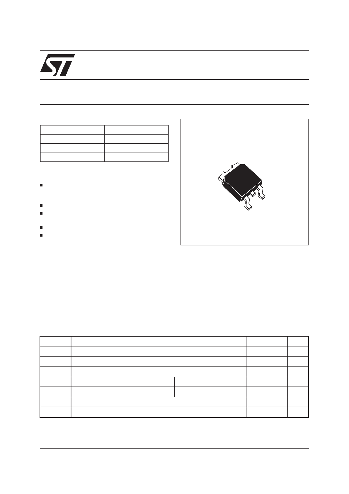
DESCRIPTION
TURBOSWITCH 1200V drastically cuts losses in
allhigh voltageoperationswhichrequire extremely
fast,soft and noise-freepower diodes.
Due to their optimized switching performances
they also highly decrease power losses in any
associated switching IGBT or MOSFET in all
”freewheelmode” operations.
K
A
NC
DPAK
They are particularly suitable in motor control
circuitries, or in primary of SMPS as snubber,
clampingor demagnetizingdiodes. They are also
suitableforthesecondaryofSMPSashighvoltage
rectifierdiodes.
ABSOLUTERATINGS
(limiting values)
Symbol Parameter Value Unit
V
RRM
V
RSM
I
F(RMS)
I
FRM
I
FSM
T
stg
T
j
TURBOSWITCHisa trademark of STMicroelectronics
November 1999 - Ed:4A
Repetitivepeakreversevoltage 1200 V
Nonrepetitivepeakreverse voltage 1200 V
RMSforward current 6 A
Repetitivepeakforwardcurrent tp = 5µs F =5kHzsquare 35 A
Surgenon repetitiveforwardcurrent tp = 10ms sinusoidal 25 A
Storagetemperaturerange - 65 to+150 °C
Maximumoperatingjunction temperature 125 °C
1/8
Page 2
STTA312B
THERMAL AND POWERDATA
Symbol Parameter Testsconditions Value Unit
R
th (j-c)
P
1
Junctiontocasethermalresistance 6.5 °C/W
Conductionpower dissipation I
= 3A,δ=0.5
F(AV)
6.7 W
Tc=80°C
P
max
Totalpowerdissipation
P
max=P1+P3
Tc=76°C 7.5 W
(P3=10%P1)
STATICELECTRICALCHARACTERISTICS
Symbol Parameter Testsconditions Min. Typ. Max. Unit
** Forwardvoltagedrop IF=3A Tj=25°C 1.8 V
V
F
I
= 3 A Tj= 125°C 1.15 1.7
F
* Reverseleakage current VR=0.8
I
R
XV
RRM
Vto Thresholdvoltage Ip < 3.I
Tj=25°C20µA
Tj=125°C 150 400
Tj=125°C 1.15 V
AV
rd Dynamicresistance 185 mΩ
Test pulses : * tp= 380 µs, δ <2%
** tp= 5 ms , δ <2%
To evaluatethe maximumconduction lossesuse thefollowingequation:
P=V
toxIF(AV)
+rdxI
F2(RMS)
µ
A
DYNAMICELECTRICALCHARACTERISTICS
TURN-OFF SWITCHING
Symbol Parameter Testconditions Min. Typ. Max. Unit
t
rr
I
RM
Maximum
recoverycurrent
Sfactor Softnessfactor Tj = 125°CV
Tj=25°CIF= 0.5A IR=1A Irr= 0.25A
I
=1A dIF/dt=50A/µs
F
V
R
Tj = 125°CIF=3A VR= 600V
dI
F
dI
F
R
dI
F
=30V
/dt = -16A/µs
/dt = -50A/µs 6.0
=600V IF=3A
/dt = -50A/µs
65
115
3.6
1.2 -
TURN-ON SWITCHING
Symbol Parameter Test conditions Min. Typ. Max. Unit
t
fr
Forwardrecovery
time
V
FP
Peakforward voltage 35 V
Tj=25°C
=3A dIF/dt = 16A/µs
I
F
Measuredat 1.1x V
900 ns
Fmax
ns
A
2/8
Page 3
STTA312B
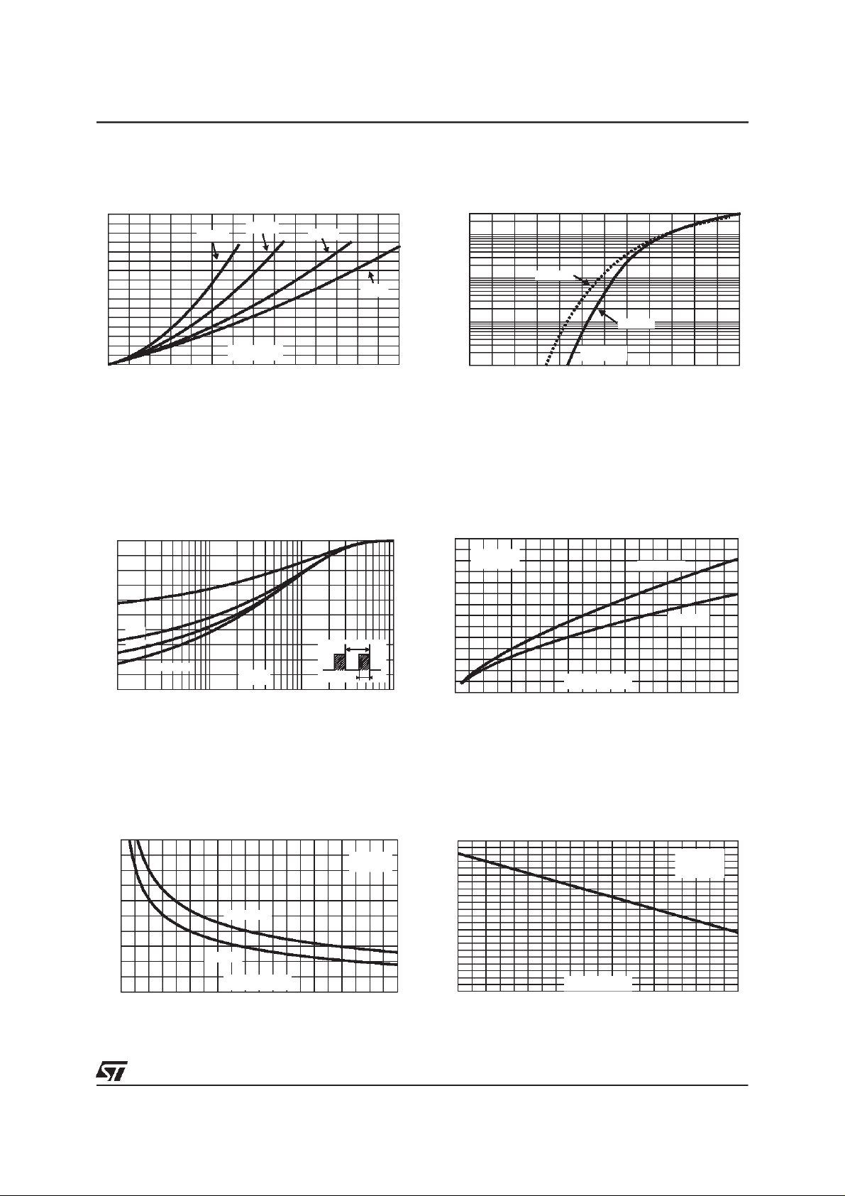
Fig.1:
Conductionlossesversusaveragecurrent.
P1(W)
8
7
δ = 0.1
δ = 0.2
δ= 0.5
6
5
4
δ =1
3
2
1
0
0.0 0.5 1.0 1.5 2.0 2.5 3.0 3.5
Fig. 3:
Relative variation of thermal impedance
IF(av) (A)
junctionto case versuspulse duration.
Zth(j-c)/Rth(j-c)
1.0
0.8
δ = 0.5
0.6
δ = 0.2
0.4
δ = 0.1
0.2
Single pulse
tp(s)
0.0
1E-3 1E-2 1E-1 1E+0
δ
=tp/T
T
tp
Fig. 2:
Forward voltage drop versus forward cur-
rent(maximumvalues).
IFM(A)
3E+1
1E+1
1E+0
1E-1
Tj=125°C
Tj=25°C
VFM(V)
1E-2
0.0 0.5 1.0 1.5 2.0 2.5 3.0
Fig.4:
PeakreverserecoverycurrentversusdI
(90%confidence).
IRM(A)
14
VR=600V
12
Tj=125°C
10
8
6
4
2
0
0 102030405060708090100
dIF/dt(A/µs)
IF=2*IF(av)
IF=IF(av)
/dt
F
Fig. 5:
Reverse recovery time versus dI
/dt (90%
F
confidence).
trr(ns)
600
VR=600V
500
400
IF=2*IF(av)
300
200
100
0 102030405060708090100
IF=IF(av)
dIF/dt(A/µs)
Tj=125°C
Fig. 6:
Softness factor tb/ta versus dI
/dt (typical
F
values).
S factor
1.6
1.5
1.4
1.3
1.2
1.1
1.0
0.9
0.8
0.7
0.6
0.5
0 102030405060708090100
dIF/dt(A/µs)
IF<2*IF(av)
VR=600V
Tj=125°C
3/8
Page 4

STTA312B
Fig. 7: Relative variation of dynamic parameters
versusjunctiontemperature(reference:Tj=125°C).
1.1
1.0
0.9
0.8
0.7
25 50 75 100 125
Fig. 9:
Forward recovery time versus dI
S factor
Tj(°C)
IRM
/dt (90%
F
confidence).
tfr(ns)
1000
900
800
VFR=1.1*VF max.
IF=IF(av)
Tj=125°C
Fig. 8: Transient peak forward voltage versus
dI
/dt(90%confidence).
F
VFP(V)
60
IF=IF(av)
Tj=125°C
50
40
30
20
10
0
0 20406080100
dIF/dt(A/µs)
700
600
500
dIF/dt(A/µs)
400
0 20406080100
4/8
Page 5

APPLICATIONDATA
TM
The 1200V TURBOSWITCH
designed to provide the lowest overall power
losses in all frequency or high pulsed current
operations.
In such application (fig. A to D), the way of
calculatingthe powerlossesis givenbelow :
series has been
TOTALLOSSES
due tothe diode
P = P1+P2+P3+ P4+P5 Watts
STTA312B
Fig. A :
CONDUCTION
LOSSES
inthe diode
”FREEWHEELMODE”
SWITCHING
TRANSISTOR
V
R
REVERSE
LOSSES
in thediode
.
t
T
SWITCHING
LOSSES
in the diode
DIODE:
TURBOSWITCH
SWITCHING
LOSSES
in thediode
due to the diode
IL
F=1/T =t/T
LOAD
5/8
Page 6

STTA312B
APPLICATIONDATA(Cont’d)
Fig.B :
Fig.D :
SNUBBERDIODE.
t
T
F = 1/T = t/T
RECTIFIERDIODE.
PWM
Fig. C:
DEMAGNETIZINGDIODE.
Fig. E :
6/8
STATICCHARACTERISTICS.
I
I
F
Rd
V
R
V
tOVF
I
R
Conductionlosses :
P1 = V
t0xIF(AV)+RdxIF2(RMS)
Reverse
V
P2 = V
losses:
RxIRx(1-
δ)
Page 7

APPLICATIONDATA(Cont’d)
STTA312B
Fig.F :
TURN-OFF CHARACTERISTICS.
V
TRANSISTOR
I
I
dI /dt
F
V
I
RM
tbta
trr = ta + tb S = tb / ta
I
dIF/dt = VR/L
V
I
RM
tbta
dI /dt
R
dI /dt
R
DIODE
RECTIFIER
OPERATION
IL
t
VR
V
Turn-onlosses :
(inthetransistor,dueto thediode)
×
I
RM
R
I
RM
×
2×
×
6
I
6
2
×(3+2 ×
xdI
F
I
×(S+ 2)×
L
d
⁄
dt
IF
2
××
RM
dI
x
F
Turn-off
P5 =
V
R
+
losses:
P3=
V
R
×
V
t
Turn-off
losses :
⁄
⁄
S)F
dt
F
S×F
dt
withnon negligibleserialinductance
V
P3’=
R
t
2
×
I
6
RM
xdI
×
⁄
F
S×F
dt
L×I
+
RM
2
2
×
F
P3, P3’ and P5 are suitable for power MOSFET
R
andIGBT
Fig.G :
trr = ta + tb
S = tb/ta
TURN-ON CHARACTERISTICS.
I
F
I
dI /dt
F
Fmax
Turn-on
P4= 0.4 (V
0
V
F
V
Fp
1.1V
F
0t
tfr
t
V
F
losses:
FP-VF
)xI
Fmaxxtfr
xF
7/8
Page 8

STTA312B
PACKAGEMECHANICAL DATA
DPAK
DIMENSIONS
REF.
Millimeters Inches
Min. Max Min. Max.
A 2.20 2.40 0.086 0.094
A1 0.90 1.10 0.035 0.043
A2 0.03 0.23 0.001 0.009
B 0.64 0.90 0.025 0.035
B2 5.20 5.40 0.204 0.212
C 0.45 0.60 0.017 0.023
C2 0.48 0.60 0.018 0.023
D 6.00 6.20 0.236 0.244
E 6.40 6.60 0.251 0.259
G 4.40 4.60 0.173 0.181
H 9.35 10.10 0.368 0.397
L2 0.80 typ. 0.031 typ.
L4 0.60 1.00 0.023 0.039
V2 0° 8° 0° 8°
FOOTPRINTDIMENSIONS
(inmillimeters)
6.7
6.7
6.7
3
1.61.6
2.32.3
Orderingtype Marking Package Weight Base qty Deliverymode
STTA312B A312 DPAK 0.3g 75 Tube
STTA312B-TR A312 DPAK 0.3g 2500 Tape& reel
Epoxymeets UL94,V0
Informationfurnished is believed to be accurateand reliable.However, STMicroelectronics assumes noresponsibility forthe consequences of
use ofsuch information nor forany infringementof patents orother rights ofthirdparties which mayresult from its use.Nolicense isgrantedby
implication or otherwise under any patent or patent rights of STMicroelectronics. Specifications mentioned in this publication are subject to
change withoutnotice. This publicationsupersedes and replaces allinformation previously supplied.
STMicroelectronics products are not authorized for use as critical components in life support devices or systems withoutexpress written approval ofSTMicroelectronics.
The ST logois a registeredtrademark ofSTMicroelectronics
1999 STMicroelectronics - Printedin Italy -All rights reserved.
STMicroelectronics GROUP OF COMPANIES
Australia - Brazil - China - Finland - France - Germany - Hong Kong - India - Italy - Japan - Malaysia
Malta - Morocco - Singapore - Spain - Sweden - Switzerland - United Kingdom - U.S.A.
http://www.st.com
8/8
 Loading...