

Page 1
®
TURBOSWITCHTM ULTRA-FAST HIGH VOLTAGE DIODE
MAIN PRODUCT CHARACTERISTI CS
STTA306B
I
F(AV)
V
RRM
(typ) 20 ns
t
rr
(max) 1.65 V
V
F
3 A
600 V
FEATURES AND BENEFITS
SPECIFIC TO FREEWHEEL MODE OPERATIONS:
FREEWHEEL OR BO OSTER DIODE.
ULTRA-FAST, AND SOF T RECOVERY.
VERY LOW OVERALL POWER LOSSES IN
BOTH THE DIODE AND THE COMPANION
TRANSISTOR.
HIGH FREQ UENC Y O PERA TIO NS.
DESCRIPTION
The TURBOSWITCH is a very high performance
series of ultra-fast high voltage power diodes.
TURBOSWITCH family drastically cuts losses in
both the diode and the associated switching IGBT
or MOSFET in all freewheel mode operations and
is particulary suitable and efficient in motor control
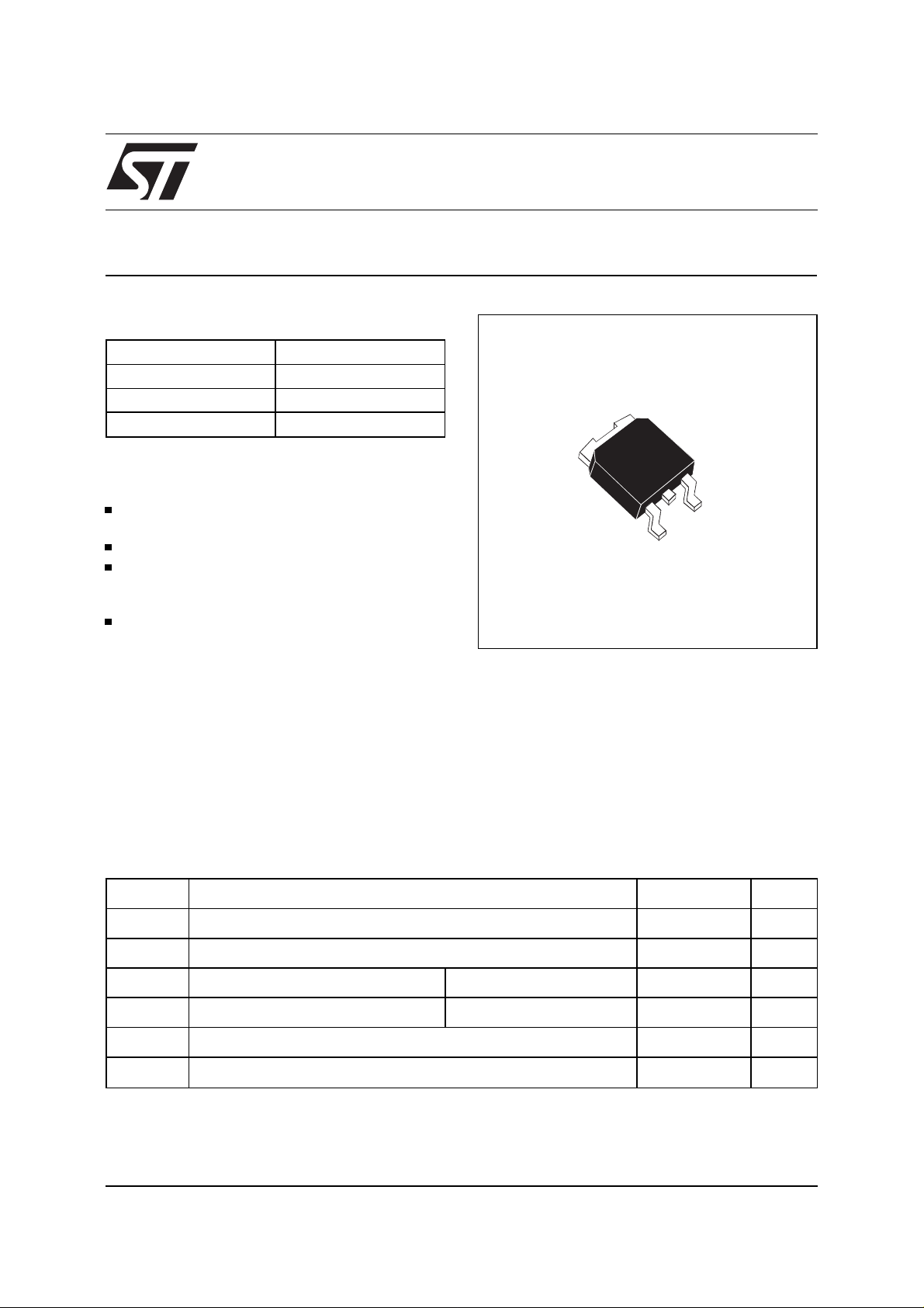
K
A
NC
DPAK
freewheel applications and in booster diode applications in Power Factor Control circuitries.
Packaged in DPAK, these 600V devices are particularly intended for use on 240V domestic mains.
ABSOLUTE RATINGS
(limiting values)
Symbol Parameter Value Unit
V
RRM
I
F(RMS)
I
FRM
I
FSM
Repetitive peak reverse voltage 600 V
RMS forward current 6 A
Repetitive peak forward current tp=5 µs F=5 kHz s quare 20 A
Surge non repetitive forward current tp=10 ms sinusoidal 35 A
Tj Maximum operating junction temper ature 125 °C
T
stg
TM : TURBOSWITCH is a trademark from STMicroelectronics
November 1999 - Ed: 3C
Storage temperature range - 65 to + 150
°
C
1/8
Page 2

STTA306B
THERMAL AND POWER DATA
Symbol Parameter Tests conditions Value Unit
R
P
th (j-c)
P
max
Junction to case 6
Conduction power dissipation I
1
Total power dissipation
P
= P1 + P3 (P3 = 10% P1)
max
= 1.5A, δ = 0.5
F(AV)
T
= 110°C
c
= 108°C 2.8 W
T
c
2.5 W
STATIC ELECTRICAL CHARACTE RISTICS
Symbol Parameter Tests conditions Min. Typ. Max. Unit
V
** Forward voltage drop Tj = 25°CIF = 3 A 1.85 V
F
I
* Reverse leakage
R
current
V
Threshold voltage Ip < 3.I
to
Tj = 125°CI
Tj = 25°CV
Tj = 125°C 500 1200
F(AV)
= 3 A 1.3 1.65
F
= 0.8 X V
R
RRM
20
Tj = 125°C 1.15 V
Rd Dynamic resistance 175 m
Test pulse : * tp = 380 µs, δ < 2%
** tp = 5 ms, δ < 2%
°
C/W
µ
A
Ω
To evaluate the maximum conduction losses use the following equation :
P = V
x I
to
F(AV)
+ Rd x I
F2(RMS)
DYNAMIC ELECTRICAL CHARACTE RISTICS
TURN-OFF SWITCHING
Symbol P arameter Test conditions Min. Typ. M ax. Unit
t
I
rr
RM
Maximu m reve rse
Tj = 25° C IF=0.5A IR=1A Irr=0.25A
Tj = 125°C IF=3A VR=400V
recover y curre nt
S factor Softness factor Tj = 125°C V
I
=1A dIF/dt= -50A/µs
F
V
=30V
R
dI
/dt = -16A/µs
F
dI
/dt = -50A/µs2.0
F
=400V IF=3A
R
dI
/dt = -50A/µs
F
20
50
1.2
1.1 -
TURN-ON SWITCHING
Symbol Parameter Test conditions Min. Typ. Max. Unit
t
fr
Forward recovery
Tj = 25°C I
time
=3A dIF/dt = 16A/µs
F
Measured at 1.1 x V
Fmax
500 ns
ns
A
2/8
V
FP
Peak forward
Tj = 25°C IF=2A dIF/dt = 16A/µs10V
voltage
Page 3
STTA306B
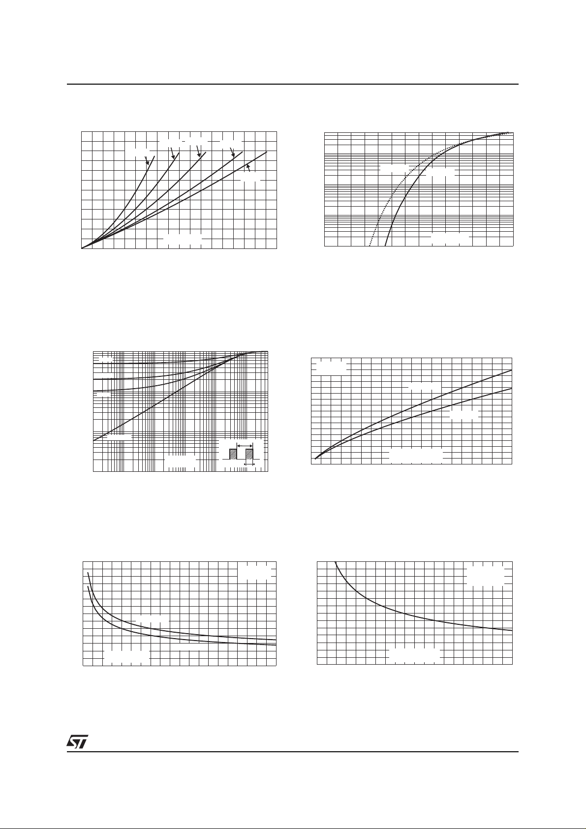
Fig. 1:
Conduction losses vers us average c urrent.
P1(W)
3.0
δ = 0.2
2.5
2.0
δ = 0.05
δ = 0.1
δ = 0.5
δ = 1
1.5
1.0
0.5
IF(av) (A)
0.0
0.0 0.2 0.4 0.6 0.8 1.0 1.2 1.4 1.6 1.8
Fig. 3:
Relative variation of thermal transient
impedance junction to ambient versus pulse
duration (recommended pad layout).
Zth(j-a) (°C/W)
1E+0
δ = 0.5
δ = 0.2
1E-1
δ = 0.1
1E-2
1E-3
Single pulse
tp(s)
1E-3 1E-2 1E-1 1E+0 1E+1 1E+2 5E+2
δ
=tp/T
T
tp
Fig. 2:
Forward voltage drop versus forward
current (maximum values).
IFM(A)
5E+1
1E+1
Tj=125°C
1E+0
1E-1
1E-2
0.0 0.5 1.0 1.5 2.0 2.5 3.0 3.5
Fig. 4:
Peak rever se recove ry curr ent vers us dI
Tj=25°C
VFM(V)
(90% confidence).
IRM(A)
9
VR=400V
8
Tj=125°C
7
6
5
4
3
2
1
0
0 20 40 60 80 100 120 140 160 180 200
IF=2*IF(av)
IF=IF(av)
dIF/dt(A/µs)
/dt
F
Fig. 5:
Reverse recovery time versus dI
/dt (90%
F
confidence).
trr(ns)
350
300
250
200
150
IF=2*IF(av)
100
50
0
dIF/dt(A/µs)
0 20 40 60 80 100 120 140 160 180 200
IF=IF(av)
VR=400V
Tj=125°C
Fig. 6:
Softn ess factor (tb/ta) versu s dI
/dt (typical
F
values).
S factor
1.6
1.4
1.2
1.0
0.8
0.6
0.4
0.2
0 20 40 60 80 100 120 140 160 180 200
dIF/dt(A/µs)
IF<2*IF(av)
VR=400V
Tj=125°C
3/8
Page 4

STTA306B
Fig. 7:
Relative variation of dynamic parameters
vers us ju n ctio n te mpe rat ure (r efer enc e T j=125° C).
1.1
1.0
0.9
0.8
0.7
25 50 75 100 125
Fig. 9:
Forwar d rec ove ry time vers us dI
S factor
Tj(°C)
IRM
/dt (90%
F
confidence).
tfr(ns)
300
250
200
IF=IF(av)
VFR=1.1*VF max.
Tj=125°C
Fig. 8:
dI
24
22
20
18
16
14
12
10
Fig. 10:
Transient peak forward voltage versus
/dt (90% confidence).
F
VFP(V)
IF=IF(av)
Tj=125°C
8
6
4
2
0
0 20 40 60 80 100 120 140 160 180 200
dIF/dt(A/µs)
Junction capacitance versus reverse
voltage applied (typical values).
C(pF)
10
5
F=1MHz
150
100
50
0
0 20 40 60 80 100 120 140 160 180 200
dIF/dt(A/µs)
2
VR(V)
1
1 10 100 200
4/8
Page 5

APPLICATION DA TA
The TURBOSWITCH
provide the lowest overall power losses in any
Freewheel Mode application (see fig. A) considering both the diode and the companion transistor,
thus optimizing the overall performance in the end
application.
TM
is especially designed to
P = P1+ P2+ P3+ P4+ P5 Watts
TOTAL LOSSES
due to the diode
STTA306B
The way of calculating the power losses is given
below :
Fig. A :
CONDUCTION
LOSSES
in the diode
"FREEWHEEL" MODE
SWITCHING
TRANSISTOR
V
R
tp
REVERSE
LOSSES
in the diode
T
SWITCHING
LOSSES
in the diode
DIODE:
TURBOSWITCH
SWITCHING
LOSSES
in the transistor
due to the diode
IL
F=1/T δ= tp/T
LOAD
5/8
Page 6

STTA306B
APPLICATION DATA (Cont’d)
Fig. B :
Fig. C :
STATIC CHARACTERISTICS
I
I
F
Rd
V
R
to
V
F
V
I
R
TURN-OFF CHARACTERIS TICS
V
TRANSISTOR
I
IL
Conduction
P1 = V
V
Reverse
P2 = V
Turn-on
x I
to
F(AV)
losses :
x I
R
R x (1 -
losses :
losses :
+ Rd x I
δ
)
F2(RMS)
(in the transistor, due to the diode)
I
I
RM
RM
×
2 ×
2
× (3 + 2 ×
dI
6
x
F
I
S
(
×
L
⁄
dI
dt
F
⁄
dt
+ 2) ×
V
×
R
P5 =
t
+
V
×
R
F
)
×
S
F
I
dI /dt
V
I
RM
I
V
I
trr = ta + tb
S=tb/ta
F
DIODE
tbta
dI /dt
R
trr = ta + tb S = tb / ta
dI /dt
R
RECTIFIER
OPERATION
dIF/dt = VR/L
tbta
RM
VR
V
t
Turn-off
t
R
losses (in the diode) :
P3 =
V
×
R
I
RM
6 x
2
× S ×
dI
F
F
⁄
dt
P3 and P5 are suitable for power MOSFET and
IGBT
6/8
Page 7

APPLICATION DA TA ( Co nt’d)
STTA306B
Fig. D :
TURN-ON CHARACTERIST ICS
I
F
I
dI /dt
F
0
V
F
V
Fp
1.1V
F
0t
tfr
Fmax
Turn-on
= 0.4 (VFP - VF) x I
P4
t
V
F
losses :
Fmax
x t
x F
fr
7/8
Page 8

STTA306B
PACKAGE MECHANICAL DATA
DPAK
DIMENSIONS
REF.
Millimeters Inches
Min. Max Min. Max.
A 2.20 2.40 0.086 0.094
A1 0.90 1.10 0.035 0.043
A2 0.03 0.23 0.001 0.009
B 0.64 0.90 0.025 0.035
B2 5.20 5.40 0.204 0.212
C 0.45 0.60 0.017 0.023
C2 0.48 0.60 0.018 0.023
D 6.00 6.20 0.236 0.244
E 6.40 6.60 0.251 0.259
G 4.40 4.60 0.173 0.181
H 9.35 10.10 0.368 0.397
L2 0.80 typ. 0.031 typ.
L4 0.60 1.00 0.023 0.039
V2 0° 8° 0° 8°
FOOTPRINT DIMENSI ON S
(in millimeters)
6.7
6.7
3
3
1.61.6
2.32.3
Ordering type Marking Package Weight Base qty Delivery mode
STTA306B A306 DPAK 0.3 g. 75 Tube
STTA306B-TR A306 DPAK 0.3 g. 2500 Tape & r eel
Epoxy meets UL94,V0
Information furnished is believed to be accurate and reliable. However, STMicroelectronics assumes no responsibility for the consequences of
use of such information nor for any infringement of patents or other rights of third parties which may result from its use. No license is granted by
implication or otherwis e under any patent or patent rights of STMicroelectro nics. Specifications men tioned in this publication are subject to
change without notice. This publication supersedes and replaces all information previously supplied.
STMicroelectro nic s products are not aut hori zed for use as critical components in l i fe s upport devices or systems without expres s written approval of STMicroelectronics.
The ST logo is a registered trademark o f STMicroelectron ics
© 1999 STMicroelectronics - Printed in Italy - All rights reserved.
STMicroelectronics GROUP OF COMPANIES
Australia - Brazil - China - Finland - France - Germany - Hong Kong - India - Italy - Japan - Malaysia
Malta - Morocco - Singapore - Spain - Sweden - Switzerland - United Kingdom - U.S.A.
http://www.st.com
8/8
 Loading...