

Page 1
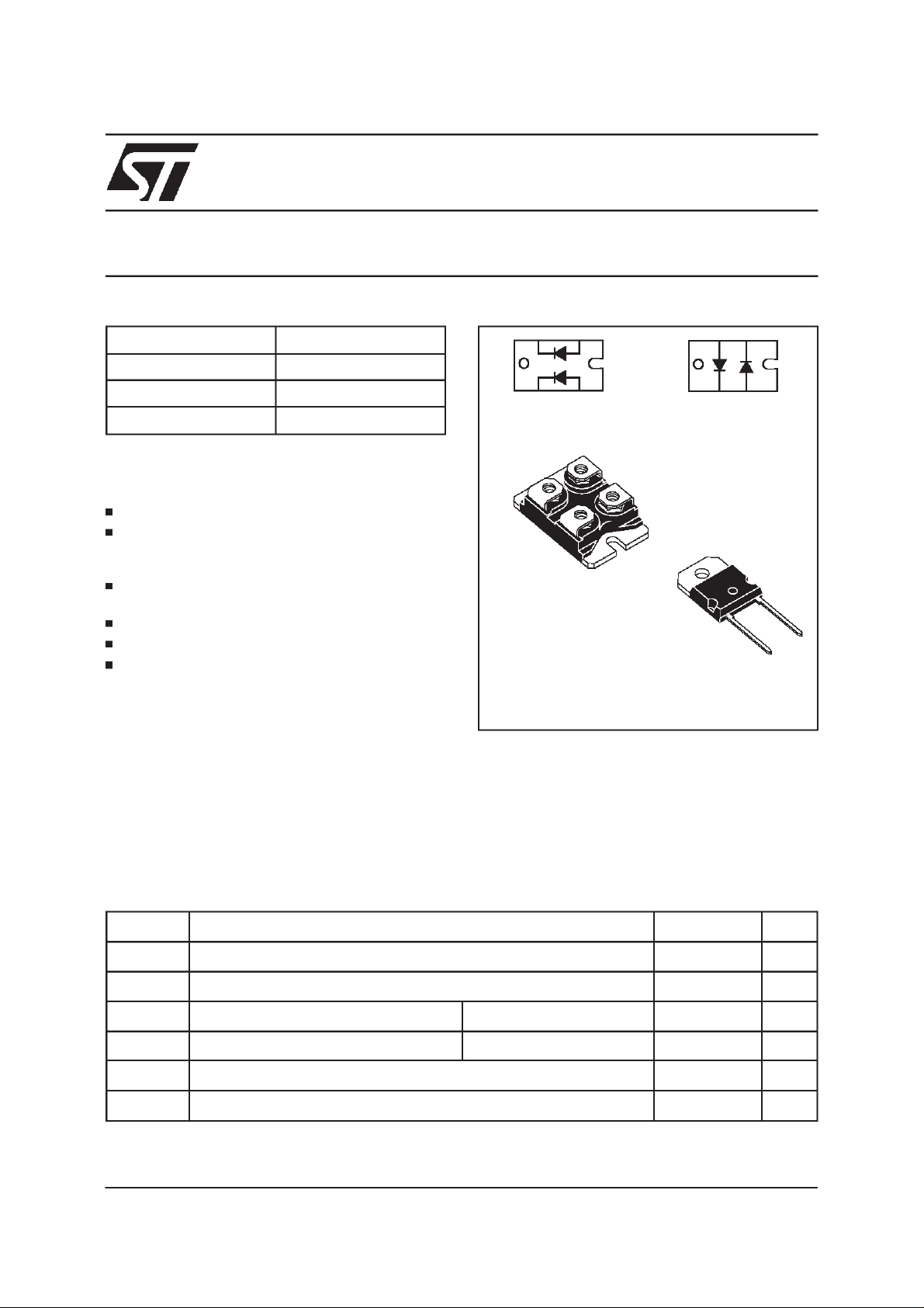
STTA2512P
TURBOSWITCH
ULTRA-FASTHIGH VOLTAGE DIODE
MAINPRODUCTCHARACTERISTICS
I
F(AV)
V
RRM
t
(typ) 60ns
rr
(max) 1.9V
V
F
25A
1200V
FEATURESAND BENEFITS
ULTRA-FAST,SOFT RECOVERY.
VERY LOW OVERALL POWER LOSSES IN
BOTH THE DIODE AND THE COMPANION
TRANSISTOR.
HIGH FREQUENCY AND/OR HIGH PULSED
CURRENTOPERATION.
HIGHREVERSEVOLTAGECAPABILITY.
LOW INDUCTANCEPACKAGE< 5 nH.
INSULATEDPACKAGE: ISOTOP
Electricalinsulation : 2500V
RMS
TM
Capacitance: < 45pF.
STTA5012TV1/2
K2 A2
K1 A1
STTA5012TV1
ISOTOP
TM
A2
K2K1A1
STTA5012TV2
K
A
K
SOD93
STTA2512P
DESCRIPTION
TURBOSWITCH 1200V drastically cuts losses in
allhighvoltageoperationswhich requireextremely
fast,soft andnoise-freepower diodes.Due to their
optimizedswitchingperformancesthey also highly
decrease power losses in any associated
switchingIGBT or MOSFET in all freewheelmode
ABSOLUTE RATINGS
(limitingvalues, perdiode)
operations.
They are particularly suitable in Motor Control
circuitries, or in the primaryof SMPS assnubber,
clampingor demagnetizingdiodes. They are also
suitable for secondary of SMPS as high voltage
rectifierdiodes.
Symbol Parameter Value Unit
V
RRM
I
F(RMS)
I
FRM
I
FSM
T
stg
T
j
ISOTOPand TURBOSWITCH are trademarks of STMicroelectronics.
November 1999 - Ed: 4B
Repetitivepeak reverse voltage 1200 V
RMSforwardcurrent 50 A
Repetitivepeak forward current tp= 5 µsF = 5kHz square 300 A
Surgenon repetitiveforwardcurrent tp= 10ms sinusoidal 210 A
Storagetemperaturerange - 65 to+ 150 °C
Maximumoperatingjunction temperature 150 °C
1/9
Page 2

STTA2512P / STTA5012TV1/2
THERMAL ANDPOWER DATA (perdiode)
Symbol Parameter Conditions Value Unit
R
th(j-c)
R
th(c)
P
1
P
max
STATICELECTRICAL CHARACTERISTICS (perdiode)
Symbol Parameter Test conditions Min Typ Max Unit
V
F
I
R
V
to
R
d
Test pulses : * tp = 380 µs, δ<2%
Junctionto casethermal
resistance
ISOTOP Perdiode 1.4 °C/W
ISOTOP Total 0.75
SOD93 1.2
Couplingthermalresistance ISOTOP Coupling 0.1 °C/W
Conductionpowerdissipation
I
=25Aδ=0.5
F(AV)
Totalpower dissipation
Pmax= P1 + P3 (P3 = 10% P1)
ISOTOP Tc=70°C57W
SOD93 Tc=82°C
ISOTOP Tc=62°C 62.5 W
SOD93 Tc=75°C
* Forward voltagedrop IF=25A Tj = 25°C
Tj = 125°C 1.3
** Reverseleakage current VR=0.8x
V
RRM
Thresholdvoltage Ip < 3.I
F(AV)
Tj = 25°C
Tj = 125°C 2.0
Tj = 125°C 1.52 V
Dynamicresistance 15 mΩ
δ
** tp = 5 ms ,
<2%
2.1
1.9
150
8
V
V
A
µ
mA
To evaluatethe maximumconductionlossesuse the following equation:
P=V
toxIF(AV)
+RdxI
F2(RMS)
DYNAMICELECTRICALCHARACTERISTICS(perdiode)
TURN-OFF SWITCHING
Symbol Parameter Testconditions Min Typ Max Unit
t
rr
Reverserecovery
time
I
RM
Maximumreverse
recoverycurrent
S factor Softnessfactor Tj= 125°CV
Tj= 25°C
= 0.5A IR=1A Irr= 0.25A
I
F
I
=1A dIF/dt =-50A/µsVR=30V
F
60
110
Tj= 125°C VR= 600V IF=25A
dI
/dt =-200 A/µs
F
/dt =-500 A/µs45
dI
F
= 600V IF=25A
R
dI
/dt =-500 A/µs 1.2
F
35
TURN-ON SWITCHING
Symbol Parameter Testconditions Min Typ Max Unit
t
fr
V
Fp
Forwardrecoverytime Tj = 25°C
=25A, dIF/dt =200 A/µs
I
F
measuredat 1.1×V
Peakforwardvoltage Tj = 25°C
=25A,dIF/dt = 200A/µs
I
F
I
=40A,dIF/dt = 500A/µs
F
max
F
900
30
35
ns
A
/
ns
V
2/9
Page 3
STTA2512P / STTA5012TV1/2
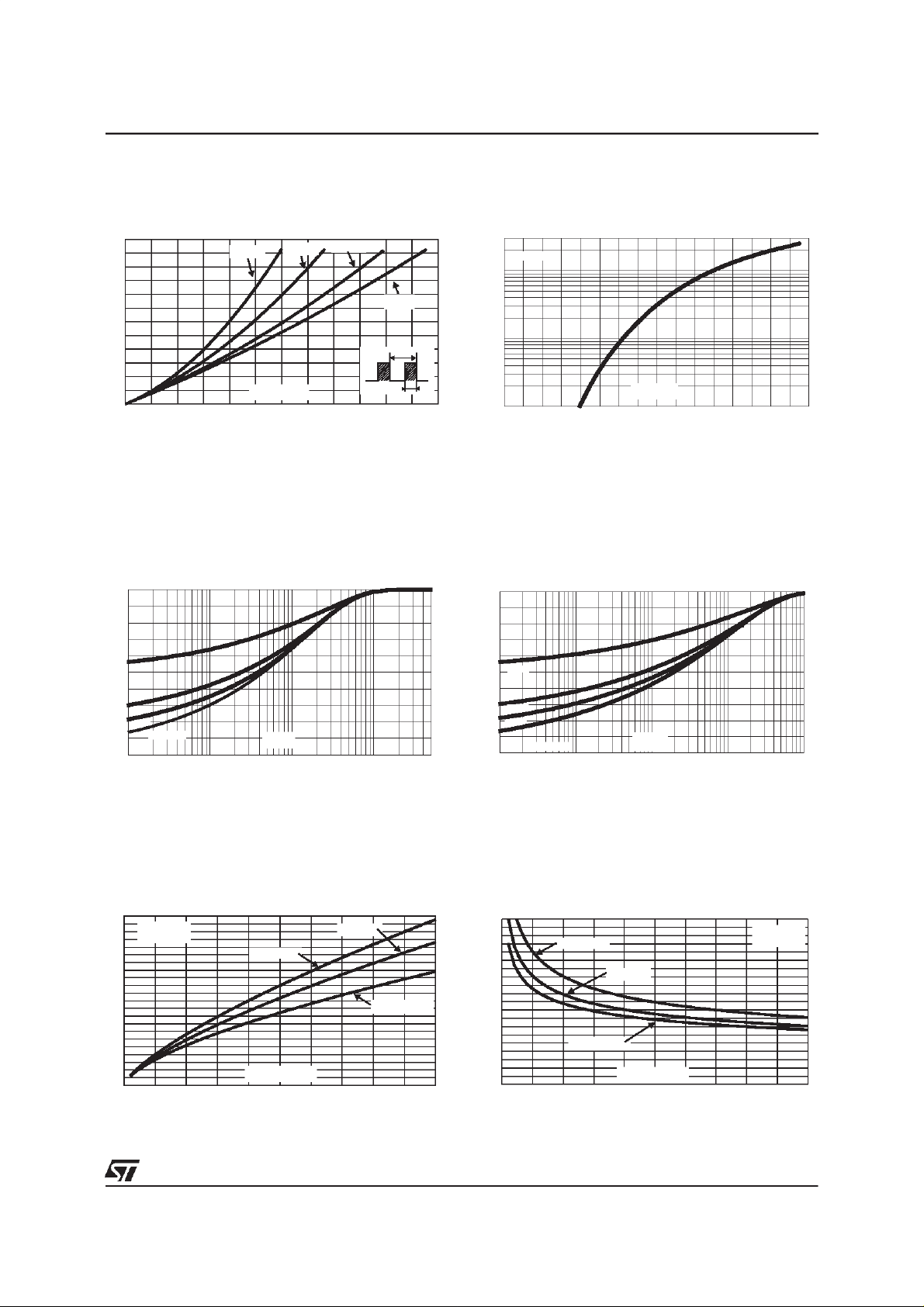
Fig. 1: Conductionlossesversusaveragecurrent
(perdiode).
P1(W)
60
δ = 0.1
δ = 0.2
δ= 0.5
50
40
δ =1
30
20
10
IF(av) (A)
0
0 5 10 15 20 25 30
T
=tp/T tp
δ
Fig.3-1:Relative variation of thermal impedance
junction to case versus pulse duration (per diode)
(ISOTOP).
Zth(j-c)/Rth(j-c)
1.0
Fig. 2: Forward voltage drop versus forward
current (maximumvalues, per diode).
IFM(A)
300
Tj=125°C
100
10
VFM(V)
1
0.0 0.5 1.0 1.5 2.0 2.5 3.0 3.5 4.0
Fig. 3-2: Relative variation of thermal impedance
junctionto caseversus pulseduration(SOD93).
Zth(j-c)/Rth(j-c)
1.0
0.8
0.6
δ = 0.5
0.4
δ = 0.2
δ = 0.1
0.2
Single pulse
0.0
1E-3 1E-2 1E-1 1E+0 5E+0
tp(s)
Fig.4: Peakreverserecoverycurrent versusdIF/dt
(90%confidence,per diode).
IRM(A)
55
VR=600V
50
Tj=125°C
45
40
IF=2*IF(av)
35
30
25
20
15
10
5
0
0 100 200 300 400 500
dIF/dt(A/µs)
IF=IF(av)
IF=0.5*IF(av)
0.8
0.6
δ = 0.5
0.4
δ = 0.2
δ = 0.1
0.2
0.0
1E-4 1E-3 1E-2 1E-1 1E+0
Single pulse
tp(s)
Fig. 5: Reverse recovery time versus dIF/dt (90%
confidence,perdiode).
trr(ns)
500
450
400
350
300
250
200
150
100
50
0
0 100 200 300 400 500
IF=2*IF(av)
IF=IF(av)
IF=0.5*IF(av)
dIF/dt(A/µs)
VR=600V
Tj=125°C
3/9
Page 4

STTA2512P / STTA5012TV1/2
Fig.6: Softnessfactor(tb/ta) versusdIF/dt (typical
values,per diode).
S factor
1.60
Tj=125°C
1.40
1.20
1.00
0.80
0 100 200 300 400 500
dIF/dt(A/µs)
IF<2*IF(av)
VR=600V
Fig. 8: Transient peak forward voltage versus
dI
/dt (90%confidence,per diode).
F
VFP(V)
60
IF=IF(av)
50
40
30
20
10
0
0 100 200 300 400 500
dIF/dt(A/µs)
Tj=125°C
Fig. 7: Relative variation of dynamic parameters
versusjunctiontemperature(reference Tj=125°C).
1.1
1.0
0.9
0.8
0.7
25 50 75 100 125
S factor
IRM
Tj(°C)
Fig. 9: Forward recovery time versus dIF/dt (90%
confidence,per diode).
tfr(ns)
1400
1200
1000
800
600
400
200
0 100 200 300 400 500
VFR=1.1*VF max.
IF=IF(av)
dIF/dt(A/µs)
Tj=125°C
4/9
Page 5

APPLICATIONDATA
The 1200V TURBOSWITCH series has been
designed to provide the lowest overall power
losses in all high frequencyor high pulsed current
operations. In such applications (Fig A to D),the
wayof calculatingthe powerlossesisgivenbelow:
TOTALLOSSES
due tothe diode
P = P1+ P2+ P3+ P4+ P5 Watts
STTA2512P / STTA5012TV1/2
CONDUCTION
LOSSES
in thediode
Fig.A : ”FREEWHEEL”MODE.
SWITCHING
TRANSISTOR
V
R
tp
REVERSE
LOSSES
in thediode
T
SWITCHING
LOSSES
in thediode
DIODE:
TURBOSWITCH
SWITCHING
LOSSES
in thetansistor
due to thediode
IL
F=1/T δ= tp/T
LOAD
5/9
Page 6

STTA2512P / STTA5012TV1/2
Fig. B : SNUBBERDIODE. Fig. C : DEMAGNETIZINGDIODE.
PWM
tp
T
F=1/T δ= tp/T
Fig.D : RECTIFIERDIODE.
STATIC& DYNAMICCHARACTERISTICS . POWERLOSSES .
Fig. E: STATICCHARACTERISTICS
6/9
I
I
F
Rd
V
R
V
to
V
F
V
I
R
Conductionlosses:
P1 = V
to.IF(AV)+Rd.IF2(RMS)
Max values at 125°C,suitablefor Ipeak< 3.IF(av)
Reverse losses:
P2 = V
R.IR
.(1-δ)
Page 7

APPLICATIONDATA (Cont’d)
Fig.F: TURN-OFFCHARACTERISTICS
STTA2512P / STTA5012TV1/2
V
I
I
dI /dt
V
I
RM
I
V
trr = ta + tb
S = tb/ta
TRANSISTOR
F
DIODE
tbta
dI /dt
R
trr = ta + tb S = tb / ta
dIF/dt = VR/L
RECTIFIER
OPERATION
tbta
dI /dt
I
RM
R
IL
t
VR
V
Turn-onlosses:
(inthe transistor,due to the diode)
2
×
I
I
RM
RM
× ( 3 + 2 ×
6
xdI
I
×
× (S+2) ×
L
2
x
dI
F
F
dt
⁄
S)×F
dt
⁄
F
P5=
+
V
R
V
×
R
Turn-offlosses(in the diode):
2
I
×
RM
6
xdI
×
⁄
F
S×F
dt
t
P3=
V
R
Turn-offlosses:
(withnon negligibleserial inductance)
2
I
V
t
R
P3’=
×
R
RM
6
xdI
×
I
L
RM
S×F
×
dt
⁄
F
2
F
×
+
2
P3,P3’and P5aresuitableforpowerMOSFETand
IGBT
Fig. G: TURN-ONCHARACTERISTICS
I
F
I
dI /dt
F
0
V
F
V
Fp
1.1V
F
0t
tfr
Fmax
t
Turn-onlosses:
P4= 0.4 (V
V
F
FP-VF
).I
Fmax.tfr
.F
7/9
Page 8

STTA2512P / STTA5012TV1/2
PACKAGEMECHANICALDATA
ISOTOP
DIMENSIONS
REF.
Millimeters Inches
Min. Max. Min. Max.
A 11.80 12.20 0.465 0.480
A1 8.90 9.10 0.350 0.358
B 7.8 8.20 0.307 0.323
C 0.75 0.85 0.030 0.033
C2 1.95 2.05 0.077 0.081
D 37.80 38.20 1.488 1.504
D1 31.50 31.70 1.240 1.248
E 25.15 25.50 0.990 1.004
E1 23.85 24.15 0.939 0.951
E2 24.80 typ. 0.976typ.
G 14.90 15.10 0.587 0.594
G1 12.60 12.80 0.496 0.504
G2 3.50 4.30 0.138 0.169
F 4.10 4.30 0.161 0.169
F1 4.60 5.00 0.181 0.197
P 4.00 4.30 0.157 0.69
P1 4.00 4.40 0.157 0.173
S 30.10 30.30 1.185 1.193
8/9
Page 9

PACKAGEMECHANICALDATA
SOD93
STTA2512P / STTA5012TV1/2
DIMENSIONS
REF.
A 4.70 4.90 0.185 0.193
C 1.17 1.37 0.046 0.054
D 2.50 0.098
D1 1.27 0.050
E 0.50 0.78 0.020 0.031
F 1.10 1.30 0.043 0.051
F3 1.75 0.069
G 10.80 11.10 0.425 0.437
H 14.70 15.20 0.578 0.598
L 12.20 0.480
L2 16.20 0.638
L3 18.0 0.709
L5 3.95 4.15 0.156 0.163
L6 31.00 1.220
O 4.00 4.10 0.157 0.161
Millimeters Inches
Min. Typ. Max. Min. Typ. Max.
Orderingtype Marking Package Weight Base qty Deliverymode
STTA5012TV1 STTA5012TV1 ISOTOP 27g.
STTA5012TV2 STTA5012TV2 ISOTOP 10 Tube
withoutscrews
10 Tube
STTA2512P STTA2512P SOD93 3.79g. 30 Tube
Coolingmethod:by conduction(C)
ISOTOP recommended torque value: 1.3 N.m. (MAX 1.5 N.m.) for the 6 x M4 screws. (2 x M4 screws
recommendedfor mountingthe packageon theheatsink andthe 4 screwsfor terminals).
ISOTOP:the screwssupplied with the package are suitable for mountingon a board witha thickness of
0.6 mmmin and 2.2mm max.
EpoxymeetsUL94,V0
Informationfurnishedis believed to be accurate and reliable.However,STMicroelectronics assumes no responsibility for the consequences of
use of such information nor forany infringementof patents or otherrights of thirdparties which may result fromits use. No licenseis grantedby
implication or otherwise under any patent or patent rights of STMicroelectronics. Specifications mentioned in this publication are subject to
change without notice. This publication supersedes and replaces all informationpreviously supplied.
STMicroelectronics products are not authorized for use as critical components in life support devices or systems without express written approval of STMicroelectronics.
The ST logois a registeredtrademark of STMicroelectronics
1999 STMicroelectronics - Printed in Italy - All rights reserved.
STMicroelectronics GROUP OF COMPANIES
Australia - Brazil - China - Finland - France - Germany - Hong Kong - India - Italy - Japan - Malaysia
Malta - Morocco - Singapore - Spain - Sweden - Switzerland - United Kingdom - U.S.A.
http://www.st.com
9/9
 Loading...