

Page 1
STTA212S
TURBOSWITCH
ULTRA-FASTHIGH VOLTAGE DIODE
MAINPRODUCTCHARACTERISTICS
I
F(AV)
V
RRM
t
(typ) 65ns
rr
(max) 1.5V
V
F
2A
1200V
FEATURESAND BENEFITS
SPECIFIC TO THE FO L LOW ING OPERAT IO N S:
SNUBBING OR CLAMPING, DEMAGHETIZATION
ANDRECTI FICATIO N
ULTRA-FASTANDSOFTRECOVERY
VERY LOW OVERALL POWER LOSSES IN
BOTH THE DIODE AND THE COMPANION
TRANSISTOR
HIGHFREQUENCY OPERATION
HIGHREVERSEVOLTAGECAPABILITY
DESCRIPTION
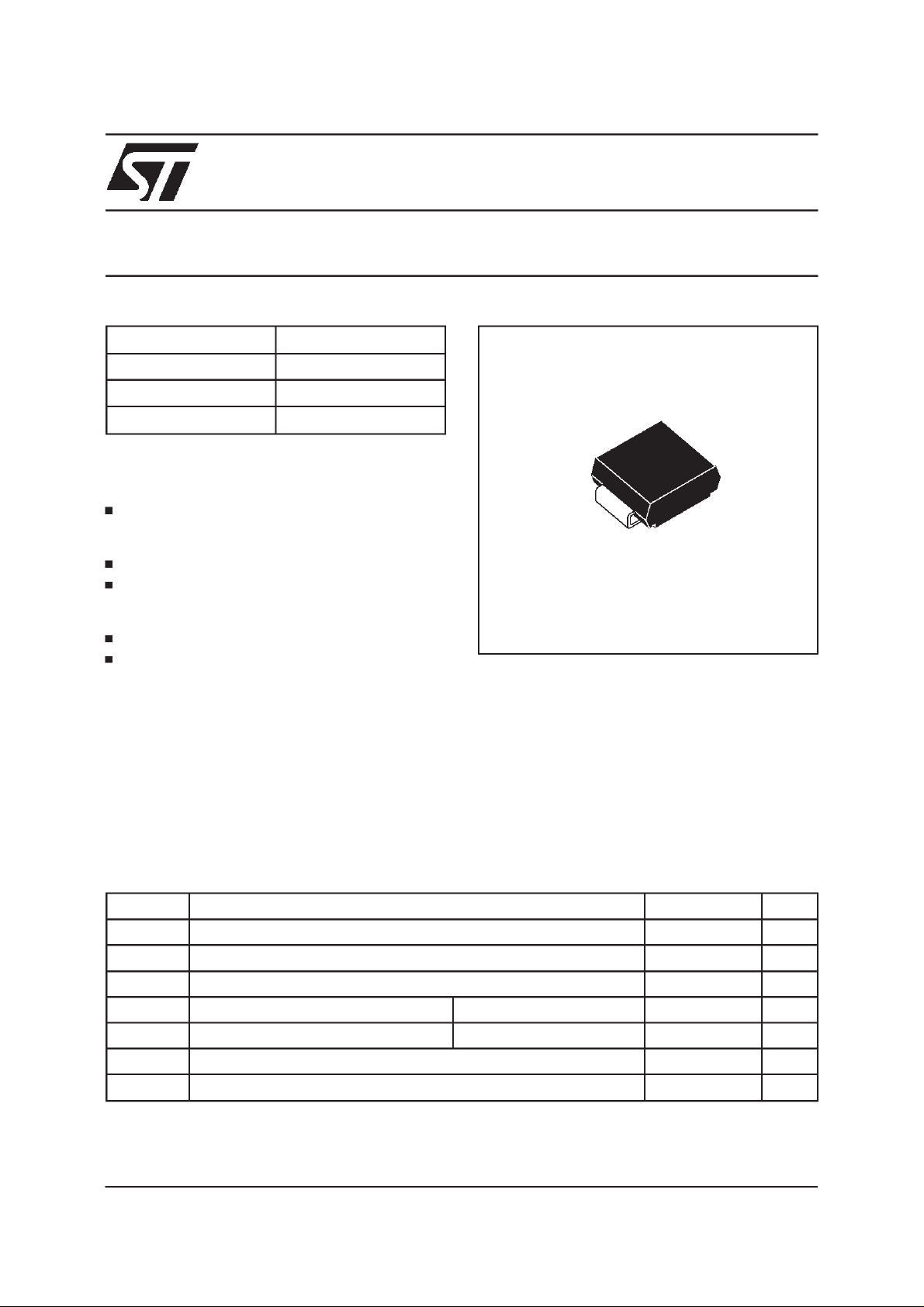
SMC
TURBOSWITCH 1200V drastically cuts losses in
all highvoltageoperationswhichrequireextremely
fast, soft and noise-freepower diodes.
Due to their optimized switching performances
they aloso highly decrease power losses in any
associated switching IGBT or MOSFET in all
suitableand efficient in motorcontrol circuitries, or
in primary of SMPS as snubber, clamping or
demagnetizingdiodes secondaryof SMPSas high
voltage rectifier diodes.They are also suitable for
the secondary of SMPS as high voltage rectifier
diodes.
”freewheel mode” operations and is particulary
ABSOLUTE RATINGS
(limitingvalues)
Symbol Parameter Value Unit
V
RRM
V
RSM
I
F(RMS)
I
FRM
I
FSM
T
stg
T
j
TURBOSWITCH is a trademark of STMicroelectronics
November 1999 - Ed:4A
Repetitivepeakreversevoltage 1200 V
Nonrepetitivepeak reversevoltage 1200 V
RMSforwardcurrent 10 A
Repetitivepeakforwardcurrent tp = 5µsF=5kHzsquare 20 A
Surgenon repetitiveforwardcurrent tp = 10mssinusoidal 25 A
Storagetemperaturerange - 65 to + 150 °C
Maximumoperatingjunction temperature 125 °C
1/8
Page 2

STTA212S
THERMAL ANDPOWERDATA
Symbol Parameter Test conditions Value Unit
R
th(j-I)
P
1
Junctionto leadthermalresistance 21 °C/W
Conductionpowerdissipation I
= 1.5A δ = 0.5
F(AV)
2.5 W
Tlead=72°C
P
max
Totalpower dissipation
Tlead=67°C 2.8 W
Pmax= P1+ P3 (P3= 10% P1)
STATICELECTRICAL CHARACTERISTICS
Symbol Parameter Test Conditions Min Typ Max Unit
V
F*
I
R**
Forwardvoltagedrop IF=2A Tj=25°C
Reverseleakagecurrent VR=0.8
xV
RRM
Vto Thresholdvoltage Ip< 3.I
Tj =125°C 1.1
Tj =25°C
Tj =125°C 15020400
Tj =125°C 1.15 V
AV
1.65
1.5
rd Dynamicresistance 175 mΩ
Test pulses : * tp = 380µs,
** tp= 5 ms ,δ<2%
δ
<2%
Toevaluate the maximum conductionlossesuse the following equation :
P=V
toxIF(AV)
+rdxI
F2(RMS)
V
A
µ
DYNAMICELECTRICAL CHARACTERISTICS
TURN-OFF SWITCHING
Symbol Parameter Testconditions Min Typ Max Unit
t
rr
I
RM
S factor Softnessfactor Tj = 125°CV
Reverserecovery
time
Maximumrecovery
current
Tj = 25°C
=0.5 A IR= 1A Irr= 0.25A
I
F
I
=1A dIF/dt=-50A/µsVR= 30V
F
65
115
Tj = 125°CVR= 600V IF=2A
/dt= -16 A/µs
dI
F
/dt= -50 A/µs 6.0
dI
F
=600V IF=2A
R
dI
/dt= -50 A/µs 0.9 /
F
3.6
TURN-ON SWITCHING
Symbol Parameter Testconditions Min Typ Max Unit
t
fr
V
Fp
Forwardrecoverytime Tj=25°C
=2A
I
Peakforwardvoltage 35 V
F
dI
/dt = 16 A/µs
F
measuredat1.1×V
max
F
900 ns
ns
A
2/8
Page 3
STTA212S
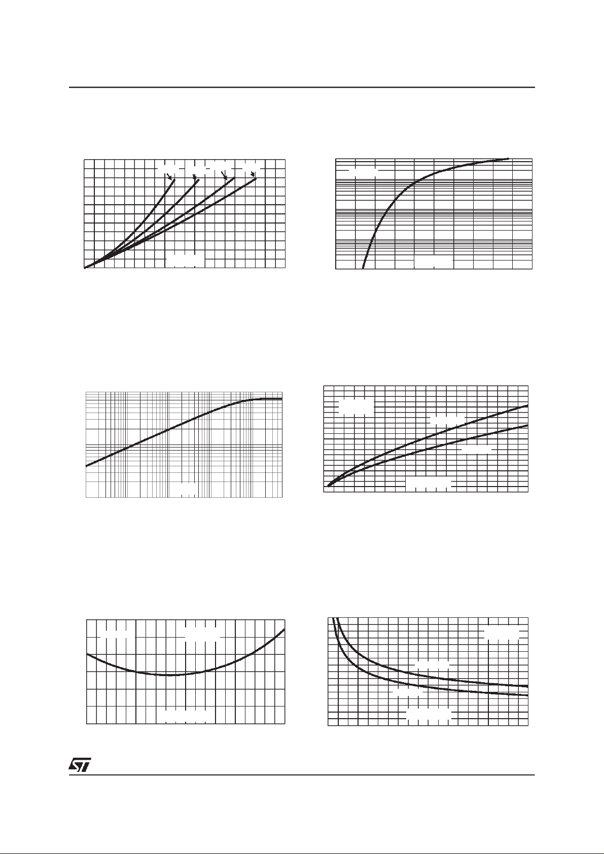
Fig.1: Conductionlosses versusaveragecurrent.
P1(W)
3.0
δ=0.1
δ=0.2
δ=0.5
δ=1
2.5
2.0
1.5
1.0
0.5
0.0
0.0 0.2 0.4 0.6 0.8 1.0 1.2 1.4 1.6 1.8 2.0
IF(av) (A)
Fig. 3: Variationof thermal impedance junctionto
ambient versus pulse duration (epoxy printed circuitboardFR4, e(Cu)=35µm,S(Cu)=1cm2).
Zth(j-a)(°C/W)
100
Fig. 2: Forward voltage drop versus forward
current (maximum values).
IFM(A)
5E+1
1E+1
Tj=125°C
1E+0
1E-1
VFM(V)
1E-2
012345
Fig.4: Peakreverserecoverycurrent versusdIF/dt
(90%confidence).
IRM(A)
20
VR=600V
Tj=125°C
15
IF=2*IF(av)
10
tp(s)
1
1E-2 5E+2
1E-1 1E+0 1E+1 1E+2
Fig. 5: Softnessfactor (tb/ta)versusdIF/dt (typical
values).
S factor
1.20
IF<2*IF(av)
1.00
0.80
0.60
0 20 40 60 80 100 120 140 160 180 200
VR=600V
Tj=125°C
dIF/dt(A/µs)
10
5
0
0 20 40 60 80 100 120 140 160 180 200
dIF/dt(A/µs)
IF=IF(av)
Fig. 6: Reverse recoverytime versus dIF/dt (90%
confidence).
trr(ns)
400
350
300
250
200
150
100
50
0
0 20 40 60 80 100 120 140 160 180 200
IF=2*IF(av)
IF=IF(av)
dIF/dt(A/µs)
VR=600V
Tj=125°C
3/8
Page 4

STTA212S
Fig. 7: Relative variation of dynamic parameters
versusjunctiontemperature(referenceTj=125°C).
1.1
1.0
S factor
0.9
IRM
0.8
Tj(°C)
0.7
25 50 75 100 125
Fig.9: Forwardrecovery timeversusdIF/dt.
tfr(ns)
800
700
VFR=1.1*VF max.
IF=IF(av)
Tj=125°C
Fig. 8: Transient peak forward voltage versus
/dt.
dI
F
VFP(V)
60
50
40
30
20
10
0
0 20406080100
IF=IF(av)
dIF/dt(A/µs)
Tj=125°C
600
500
400
300
200
0 20406080100
dIF/dt(A/µs)
4/8
Page 5

APPLICATIONDATA
STTA212S
The 1200V TURBOSWITCH has been designed
toprovidethe lowest overallpowerlossesin anyall
highfrequencyor highpulsedcurrentoperations.
TOTALLOSSES
due to the diode
P = P1+ P2+ P3+ P4+ P5 Watts
CONDUCTION
LOSSES
in the diode
REVERSE
LOSSES
in thediode
In such applications (fig. A to D), the way of
calculatingthepowerlossesis givenbelow:
SWITCHING
LOSSES
in thediode
SWITCHING
LOSSES
in the transistor
due tothe diode
Fig.A : ”FREEWHEEL”MODE
SWITCHING
TRANSISTOR
V
R
F=1/T =t/T
IL
DIODE:
TURBOSWITCH
t
T
LOAD
5/8
Page 6

STTA212S
APPLICATIONDATA (Cont’d)
Fig. B : SNUBBERDIODE. Fig. C : DEMAGNETIZINGDIODE.
PWM
t
T
F = 1/T = t/T
Fig.D : RECTIFIERDIODE.
Fig.E : STATICCHARACTERISTICS
I
I
F
Rd
V
R
V
tOVF
I
R
6/8
Conductionlosses :
P1 = V
t0xIF(AV)+RdxIF2(RMS)
Reverse losses:
P2 = V
RxIR x (1 -
V
)
δ
Page 7

APPLICATIONDATA (Cont’d)
Fig.F : TURN-OFFCHARACTERISTICS
STTA212S
V
Turn-onlosses:
(inthe transistor,duetothediode)
IL
V
TRANSISTOR
I
t
P5=
+
R
V
×
R
2
×
I
×(3 + 2×S)×
RM
6
x
I
×
I
RM
L
2
dI
×
dI
dt
⁄
F
× (S+ 2) ×
dt
⁄
F
F
F
I
dI /dt
F
DIODE
Turn-offlosses (inthediode) :
V
I
RM
I
tbta
dI /dt
R
trr = ta + tb S = tb / ta
dIF/dt = VR/L
RECTIFIER
OPERATION
VR
t
P3 =
V
R
2
I
×
6
RM
xdI
×S×
F
F
⁄
dt
V
I
trr = ta + tb
S = tb/ta
RM
tbta
dI /dt
R
Fig. G : TURN-ONCHARACTERISTICS
I
F
I
dI /dt
F
0
V
F
V
Fp
1.1V
F
0t
tfr
Fmax
t
V
R
withnon negligibleserial inductance
P3’ =
P3, P3’ and P5 are suitable for power MOSFET
andIGBT
Turn-onlosses:
Turn-offlosses:
t
V
F
P4= 0.4 (V
V
×
R
6
FP-VF
I
RM
xdI
)xI
2
×
S×F
dt
⁄
F
Fmaxxtfr
+
xF
L×I
RM
2
2
×
F
7/8
Page 8

STTA212S
PACKAGEMECHANICAL DATA
SMC
E1
D
E
A1
C
E2
L
A2
FOOTPRINTDIMENSIONS(in millimeters)
SMCPlastic
3.3
DIMENSIONS
REF.
Millimeters Inches
Min. Max. Min. Max.
A1 1.90 2.45 0.075 0.096
A2 0.05 0.20 0.002 0.008
b 2.90 3.2 0.114 0.126
c 0.15 0.41 0.006 0.016
E 7.75 8.15 0.305 0.321
E1 6.60 7.15 0.260 0.281
E2 4.40 4.70 0.173 0.185
D 5.55 6.25 0.218 0.246
b
L 0.75 1.60 0.030 0.063
2.0 4.2 2.0
Orderingtype Marking Package Weight Base qty Deliverymode
STTA212S T53 SMC 0.243g 2500 Tape& reel
EpoxymeetsUL94,V0
Bandindicatescathode
Informationfurnished is believedto be accurateandreliable.However, STMicroelectronics assumes no responsibility for the consequences of
use ofsuch informationnor forany infringementof patents orother rights of third parties which may result from its use.Nolicense is grantedby
implication or otherwise under any patent or patent rights of STMicroelectronics. Specifications mentioned in this publicationare subject to
change without notice.This publicationsupersedes and replacesall informationpreviously supplied.
STMicroelectronics products are not authorized for use as criticalcomponentsin lifesupport devices or systems without express writtenapproval of STMicroelectronics.
The ST logois a registered trademark of STMicroelectronics
1999 STMicroelectronics - Printed in Italy - Allrights reserved.
STMicroelectronics GROUP OF COMPANIES
Australia - Brazil - China - Finland - France - Germany - Hong Kong - India - Italy - Japan - Malaysia
Malta - Morocco - Singapore - Spain - Sweden - Switzerland - United Kingdom - U.S.A.
http://www.st.com
8/8
 Loading...