

Page 1
®
STTA206S
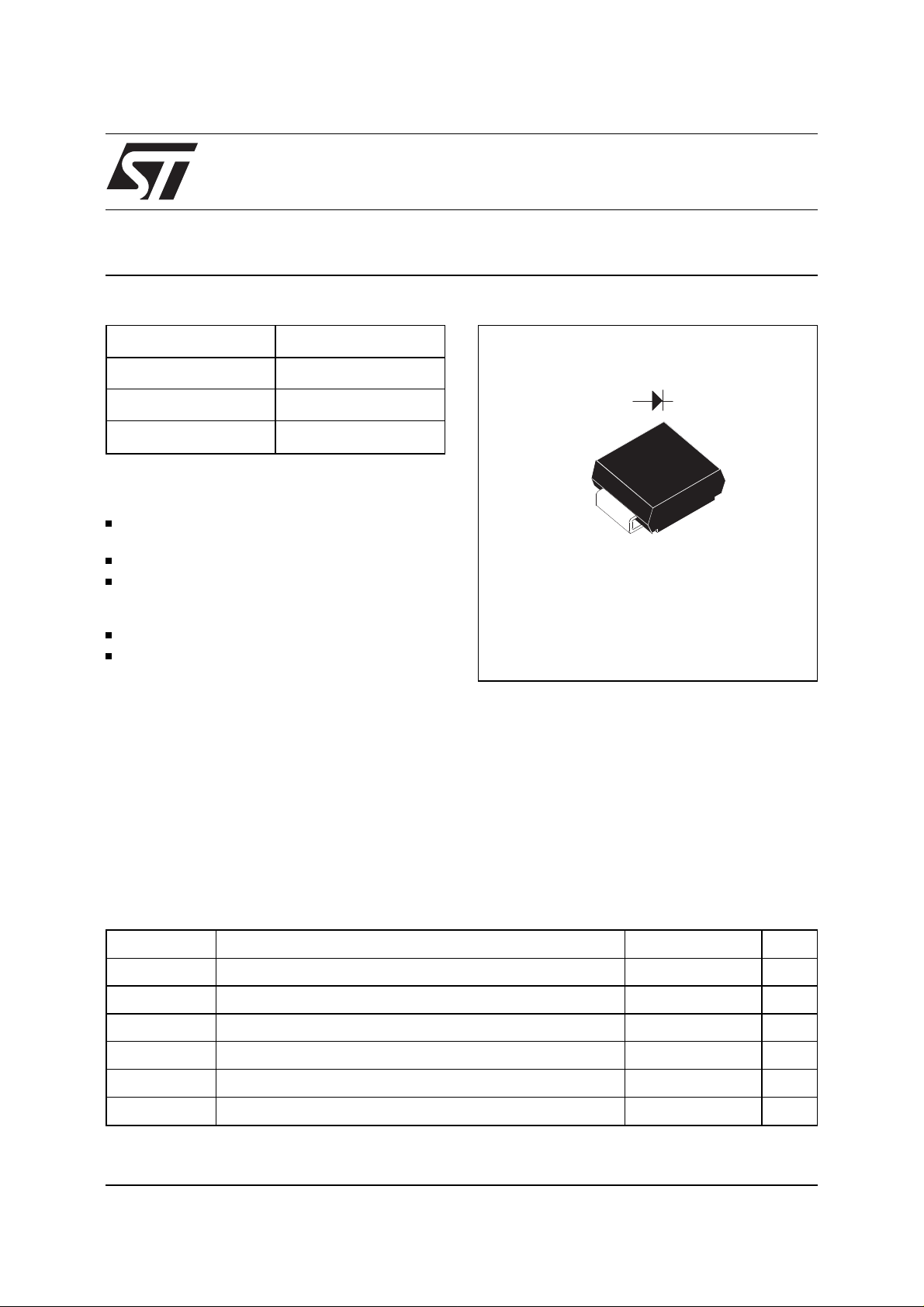
TURBOSWITCH "A". ULTRA-FAST HIGH VOLTAGE DIODE
MAIN PRODUCTS CHARACTE RISTICS
I
F(AV)
V
RRM
(typ) 20ns
t
rr
V
(max) 1.5V
F
2A
600V
FEATURES AND BENEFITS
SPECIFIC TO "FREEWHEEL MODE" OPERATIONS : FREEWHEEL OR BOOSTER DIODE
ULTRA-FAST AND SOFT RECOVERY
VERY LOW OVERALL POWER LOSSES IN
BOTH THE DIODE AND THE COMPANION
TRANSISTOR
HIGH FREQUENCY OPERATIONS
SURFACE M OUNT DE V ICE
DESCRIPTION
The TURBOSWITCH is a very high performance
series of ultra-fast high voltage power diodes from
600V to 1200V.
TURBOSWITCH "A" family drastically cuts losses
in both the diode and the associated switching
IGBT or MOSFET in all "Freewheel Mode"
operations and is particulary s uitable and efficient
AK
SMC
in Motor Control Freewheel applications and in
Booster diode applications in Power Factor Control
circuitries.
Packaged in SMC surface mount envelope, these
600V devices are particularly intended for use on
240V domestic mains.
ABSOLUTE MAXIMUM RATINGS
Symbol Parameter Value Unit
V
RRM
V
RSM
I
F(RMS)
I
FRM
T
j
T
stg
TM : TURBOSWITCH is a trademark of STMicroelectronics
November 1999 - Ed: 2D
Repetitive peak reverse voltage 600 V
Non repetitive peak reverse voltage 600 V
RMS forward current 8 A
Repetitive peak forward current (tp = 5 µs, f = 5kHz) 50 A
Maximum operating junction temperature 125 ° C
Storage temperature range - 65 to + 150 ° C
1/8
Page 2

STTA206S
THERMAL AND P OW ER DATA
Symbol Parameter Conditions Value Unit
R
P
th(j-I)
P
1
max
Junction to lead 21 °C/ W
Conduction power dissipation
(see fig. 2)
Total power dissipation
I
= 1.5A δ = 0.5
F(AV)
2.5 W
Tlead= 72°C
Tlead= 67°C 2.8 W
Pmax = P1 + P3 (P3 = 10% P1)
STATIC ELECTRICAL CHARACTE RISTICS (see Fig. 2)
Symbol Parameter Test Conditions Min Typ Max Unit
V
F *
I
R **
Test pulses widths : * tp = 380 µs, duty cy cle < 2%
Forward voltage drop IF = 2A Tj = 25°C
Reve rse le akag e curre nt VR = 0.8
** tp = 5 ms , duty cycle < 2%
x V
RRM
Tj = 125°C 1.1
Tj = 25°C
Tj = 125°C 400201200
1.75
1.5
DYNAMIC ELECTRICAL CHARACTE RISTICS
TURN-OFF SWITCHING (see Fig. 3)
Symbol Parameter Test Conditions Min Typ Max Unit
V
A
µ
t
rr
Reverse
recover y time
I
RM
Maximum
recover y curre nt
S factor Softness factor Tj = 125° C V
Tj = 25°C
I
= 0.5 A IR = 1A Irr = 0.25A
F
I
= 1 A dIF/dt =-50A/µs VR = 30V
F
20
50
Tj = 125°C VR = 400V IF = 2A
dI
/dt = -16 A/µs
F
dI
/dt = -50 A/µs2.0
F
= 400V IF = 2A
R
dI
/dt = -50 A/µsTBD-
F
1.2
TURN-ON SWITCHING (see Fig.8)
Symbol Parameter Test Conditions Min Typ Max Unit
t
fr
Forward
recove ry time
V
Fp
Peak forward
Tj = 25°C
I
= 1 A
F
dI
/dt = 8 A/µs
F
measured at, 1.1
VF max
×
500 ns
10 V
voltage
ns
A
2/8
Page 3
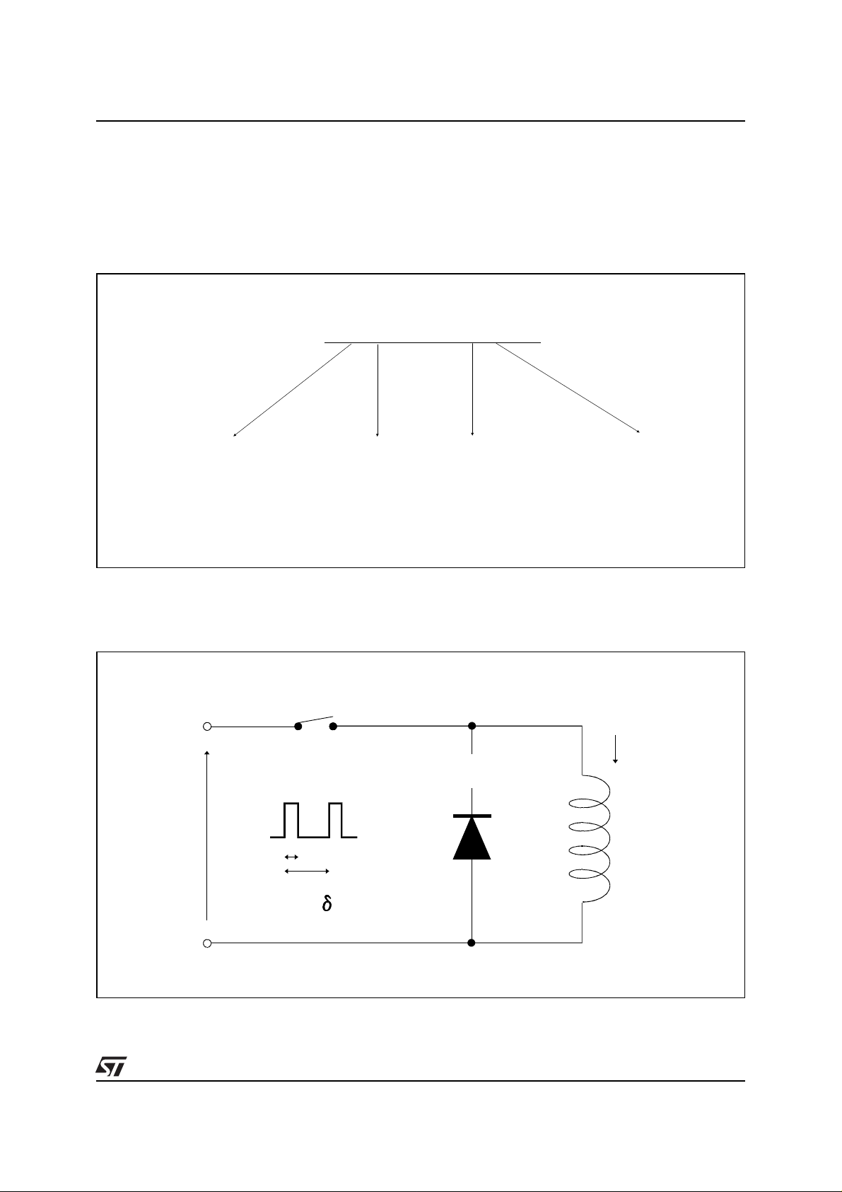
APPLICATION DA TA
The TURBOSWITCH
TM
"A" is especially
designed to provide the lowest overall power
losses in any "Freewheel Mode" application (see
fig. 1) considering both the diode and the
companion transistor, thus optimizing the overall
performance in the end application.
TOTAL LOSSES
due to the diode
P = P1+ P2+ P3+ P4+ P5 Watts
STTA206S
The way of calculating the power losses is given
below :
Fig. 1 :
CONDUCTION
LOSSES
in the diode
P1 Watts
(Fig . 2)
"FREEWHEEL" MODE
SWITCHING
TRANSISTOR
V
R
REVERSE
LOSSES
in the diode
P2 Watt s
(Fig. 2)
t
T
SWITCHING
LOSSES
in the diode
OFF : P3 Watts
ON : P4 W atts
(Fig. 3 & 4)
DIODE:
TURBOSWITCH "A"
SWITCHING
LOSSES
in the transistor
due to the diode
P2 Watts
(Fig . 3)
IL
F=1/T =t/T
LOAD
3/8
Page 4

STTA206S
APPLICATION DATA (Cont’d)
Fig. 2 :
Fig. 3 :
STATIC CHARACTERISTICS
I
I
F
Rd
V
R
V
tOVF
I
R
TURN-OFF CHARACTERISTI CS
V
TRANSISTOR
I
IL
t0
x I
losses :
F(AV)
+ Rd x I
F2(RMS)
Conduction
P1 = V
with
Vt0 = 1.15 V
R
= 0.175 Ohm
d
V
Reverse
P2 = V
R
Turn-on
(Max values at 125°C)
losses :
x I
R x (1 -
)
δ
losses :
(in the transistor, due to the diode)
I
I
RM
RM
2 ×
2
× (3 + 2 ×
6
dI
x
F
×
×
I
(
L
dI
⁄
F
dt
⁄
+ 2) ×
S
dt
×
V
+
R
×
V
R
P5 =
t
F
S
)
×
F
I
dI /dt
V
I
RM
I
V
I
trr = ta + tb
S=tb/ta
F
DIODE
tbta
dI /dt
R
trr = ta + tb S = tb / ta
dIF/dt = VR/L
tbta
RM
dI /dt
RECTIFIER
OPERATION
R
VR
V
t
Turn-off
t
R
losses (in the diode) :
P3 =
×
V
R
I
RM
6 x
2
× S ×
dI
F
F
dt
⁄
P3 and P5 are suitable for power MOSFET and
IGBT
4/8
Page 5

APPLICATION DA TA ( Co nt’d)
STTA206S
Fig. 4 :
TURN-ON CHARACTERIST ICS
I
F
I
dI /dt
F
0
V
F
V
Fp
1.1V
F
0t
tfr
Fmax
t
V
F
Ratings and characteristics curves are ON
GOING.
Conduction losses versus average current.
Fig. 5:
P1(W)
3.0
2.5
2.0
1.5
1.0
0.5
0.0
0.0 0.2 0.4 0.6 0.8 1.0 1.2 1.4 1.6 1.8 2.0
δ = 0.05
δ = 0.1
IF(av) (A)
δ = 0.2
δ = 0.5
δ = 1
Turn-on
P4
Fig. 6:
0.35
0.30
0.25
0.20
0.15
0.10
0.05
0.00
losses :
= 0.4 (VFP - VF) x I
Fmax
x t
x F
fr
Switching OFF losses versus dIF/dt.
P3(W)
Tj=125°C
F=20KHz
VR=400V
dIF/dt(A/us)
0 20 40 60 80 100 120 140 160 180 200
IL=4A
IL=2A
Switching ON los ses v ers us dIF/dt.
Fig. 7:
P4(W)
0.2
Tj=125°C F=100KHz IF=IF(AV)
0.15
0.1
0.05
0
0 20 40 60 80 100 120 140 160 180 200
dIF/dt(A/us)
Switching losses in t ransistor d ue to the diode.
Fig. 8:
P5(W)
5.0
Tj=125°C F=20KHz VR=400V
4.5
4.0
3.5
3.0
2.5
2.0
1.5
1.0
0.5
0.0
0 20 40 60 80 100 120 140 160 180 200
dIF/dt(A/us)
IL=4A
IL=2A
5/8
Page 6

STTA206S
Fig. 9:
Forward voltage drop versus forward
current (maximum values).
IFM(A)
5E+1
1E+1
1E+0
Tj=125°C
Tj=25°C
1E-1
VFM(V)
1E-2
0.0 0.5 1.0 1.5 2.0 2.5 3.0 3.5
Fig. 11:
Peak reverse recovery current versus
dIF/dt (90% confidence).
IRM(A)
10
9
VR=400V
Tj=125°C
8
7
6
5
4
3
2
1
0
0 50 100 150 200
dIF/dt(A/µs)
IF=2*IF(av)
IF=IF(av)
Fig. 10:
Relative variation of thermal impedance
junction to ambient versus pulse duration
(recommended pad layout).
Zth(j-a) (°C/W)
1E+0
δ = 0.5
δ = 0.2
δ = 0.1
1E-1
Single pulse
tp(s)
1E-2
1E-3 1E-2 1E-1 1E+0 1E+1 1E+2 5E+2
Fig. 12:
Reverse reco very time versus dI F/dt (90%
δ
=tp/T
T
tp
confidence).
trr(ns)
300
250
200
150
100
IF=2*IF(av)
50
0
0 20 40 60 80 100 120 140 160 180 200
dIF/dt(A/µs)
IF=IF(av)
VR=400V
Tj=125°C
Fig. 13:
Softness factor (tb/ta) versus dIF/dt
(typical values).
S factor
1.8
1.6
1.4
1.2
1.0
0.8
0.6
0 20 40 60 80 100 120 140 160 180 200
dIF/dt(A/µs)
6/8
IF<2*IF(av)
VR=400V
Tj=125°C
Fig. 14:
Relative variation of dynamic parameters
vers us junc tio n tem per at ure (re fere nce Tj=125°C).
1.1
1.0
0.9
0.8
0.7
25 50 75 100 125
S factor
IRM
Tj(°C)
Page 7

STTA206S
Fig. 15:
Transient peak forward voltage versus
dIF/dt (90% confidence).
VFP(V)
22
IF=IF(av)
20
Tj=125°C
18
16
14
12
10
8
6
4
2
0
0 20 40 60 80 100 120 140 160 180 200
Fig. 17:
Junction capacitance versus reverse
dIF/dt(A/µs)
voltage applied (typical values).
C(pF)
10
5
F=1MHz
Fig. 16:
Forward recovery time versus dI F/dt (90%
confidence).
tfr(ns)
300
250
200
150
100
50
0
0 20 40 60 80 100 120 140 160 180 200
dIF/dt(A/µs)
IF=IF(av)
Vfr=1.1*VFmax
Tj=125°C
2
VR(V)
1
1 10 100 200
7/8
Page 8

STTA206S
PACKAGE ME CHANICAL D AT A
SMC
E1
REF.
DIMENSIONS
Millimeters Inches
Min. Max. Min. Max.
E
C
E2
L
FOOTPRINT DIMENSIONS
D
A1
A2
(in millimeters)
3.3
A1 1.90 2.45 0.075 0.096
A2 0.05 0.20 0.002 0.008
b 2.90 3.2 0.114 0.126
c 0.15 0.41 0.006 0.016
E 7.75 8.15 0.305 0.321
E1 6.60 7.15 0.260 0.281
E2 4.40 4.70 0.173 0.185
b
D 5.55 6.25 0.218 0.246
2.0 4.2 2.0
Type Marking Package Weight Base qty Delivery mode
STTA206S T51 SMC 0.243g 2500 Tape & Reel
Band indicates cathode
Epoxy meets UL94, V0
Information furnished is believed to be accurate and reliable. However, STMicroelectronics assumes no responsibility for the consequences of
use of such information nor for any infringement of patents or other rights of third parties which may result from its use. No license is granted by
implication or otherwis e under any patent or patent rights of STMicroelec tronics. Specificati ons mentioned in this publication are subject to
change without notice. This publication supersedes and replaces all information previously supplied.
STMicroelectronics products ar e not authorized for use as critical components in life support devices or sys tems without expres s written approval of STMicroelectronics.
The ST logo is a registered trademark of S TMicroelectron ics
© 1999 STMicroelectronics - Printed in Italy - All rights reserved.
STMicroelectronics GROUP OF COMPANIES
Australia - Brazil - China - Finland - France - Germany - Hong Kong - India - Italy - Japan - Malaysia
Malta - Morocco - Singapore - Spain - Sweden - Switzerland - United Kingdom - U.S.A.
http://www.st.com
8/8
 Loading...