

Page 1

STTA1512P/PI
TURBOSWITCH
ULTRA-FASTHIGH VOLTAGE DIODE
MAINPRODUCTCHARACTERISTICS
I
F(AV)
V
RRM
t
(typ) 55ns
rr
(max) 1.9V
V
F
15A
1200V
FEATURESAND BENEFITS
ULTRA-FAST,SOFT RECOVERY.
VERY LOW OVERALL POWER LOSSES IN
BOTH THE DIODE AND THE COMPANION
TRANSISTOR.
HIGH FREQUENCY AND/OR HIGH PULSED
CURRENTOPERATION.
HIGHREVERSEVOLTAGECAPABILITY
INSULATEDPACKAGE: DOP3I
Electricalinsulation : 2500V
RMS
Capacitance: 12pF
DESCRIPTION
K
SOD93
STTA1512P
A
K
A
K
Isolated
DOP3I
STTA1512PI
TURBOSWITCH 1200V drastically cuts losses in
allhighvoltageoperationswhich requireextremely
fast,softandnoise-freepowerdiodes.Dueto their
optimizedswitchingperformancestheyalsohighly
decrease power losses in any associated
They are particularly suitable in motor control
circuitries, or in the primaryof SMPS as snubber,
clampingor demagnetizingdiodes.They are also
suitable for secondary of SMPS as high voltage
rectifierdiodes.
switchingIGBT or MOSFET in all freewheelmode
operations.
ABSOLUTE RATINGS
(limitingvalues)
Symbol Parameter Value Unit
V
RRM
I
F(RMS)
I
FRM
I
FSM
T
stg
T
j
TURBOSWITCH is a trademark of STMicroelectronics
November 1999 - Ed:5A
Repetitivepeakreversevoltage 1200 V
RMSforwardcurrent 50 A
Repetitivepeakforwardcurrent tp = 5 µsF =5kHzsquare 220 A
Surgenonrepetitiveforwardcurrent tp = 10ms sinusoidal 150 A
Storagetemperaturerange - 65 to + 150 °C
Maximumoperatingjunctiontemperature 150 °C
1/9
Page 2

STTA1512P/PI
THERMAL ANDPOWERDATA
Symbol Parameter Conditions Value Unit
R
th(j-c)
Junctionto casethermalresistance SOD93
DOP3I
P
P
max
1
Conductionpowerdissipation
I
=15Aδ=0.5
F(AV)
Totalpower dissipation
Pmax= P1+ P3 (P3 =10% P1)
SOD93
DOP3I
SOD93
DOP3I
Tc=95°C
Tc=78°C
Tc=89
Tc=70°C
STATICELECTRICAL CHARACTERISTICS
Symbol Parameter Testconditions Min Typ Max Unit
V
F*
Forwardvoltagedrop IF=15A Tj=25°C
Tj= 125°C 1.3
I
R**
Reverseleakagecurrent VR=0.8x
V
RRM
Vto Thresholdvoltage Ip < 3.I
F(AV
Tj= 25°C
Tj= 125°C 1.3
) Tj= 125°C 1.48 V
Rd Dynamicresistance Tj= 125°C25m
Test pulses : * tp= 380 µs, δ <2%
** tp= 5 ms , δ <2%
1.6
°C/W
2.1
34 W
38 W
2.1
1.9
100
6.0
µA
mA
V
V
Ω
To evaluatethe maximumconductionlosses use the followingequation :
P=V
toxIF(AV)
+RdxI
F2(RMS)
DYNAMICELECTRICALCHARACTERISTICS
TURN-OFF SWITCHING
Symbol Parameter Test conditions Min Typ Max Unit
S
t
rr
I
RM
factor
Reverserecovery
time
Maximumreverse
recoverycurrent
Tj = 25°C
=0.5 A IR= 1A Irr= 0.25A
I
F
=1A dIF/dt=-50A/µsVR=30V
I
F
Tj = 125°C VR= 600V IF=15A
dI
/dt= -120A/µs
F
/dt= -500A/µs33
dI
F
Softnessfactor Tj = 125°CVR=600V IF=15A
dI
/dt= -500A/µs 1.2
F
55
105
20
TURN-ON SWITCHING
Symbol Parameter Testconditions Min Typ Max Unit
t
fr
V
Fp
Forwardrecoverytime Tj= 25°C
=15A, dIF/dt = 120A/µs
I
F
measuredat1.1×V
Peakforwardvoltage Tj= 25°C
=15A,dIF/dt = 120A/µs
I
F
I
=40A,dIF/dt = 500A/µs
F
max
F
900
30
40
ns
A
/
ns
V
2/9
Page 3
STTA1512P/PI
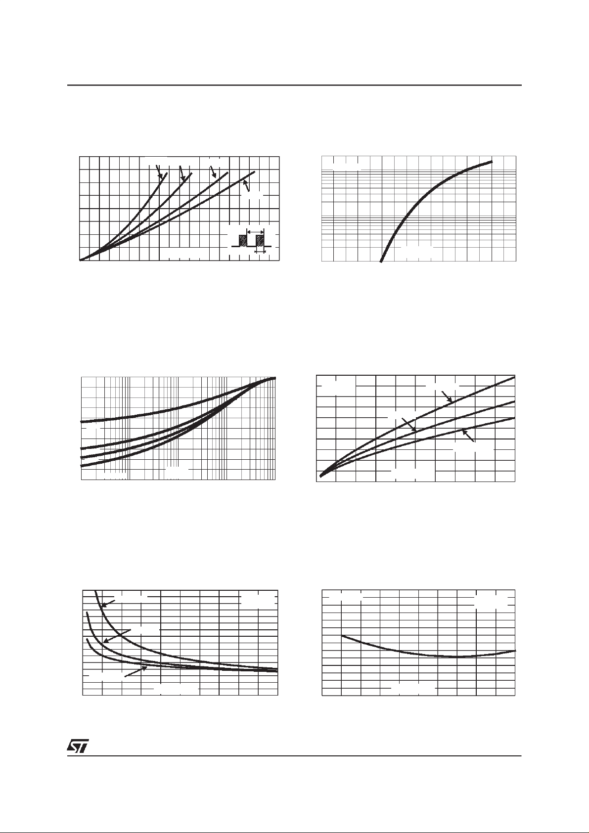
Fig. 1: Conduction losses versus average
current.
P1(W)
40
δ = 0.1
δ = 0.2
δ =0.5
30
δ = 0.1
20
δ
=tp/T
T
tp
10
0
02468101214161820
IF(av) (A)
Fig. 3: Relative variation of thermal impedance
junctionto case versus pulse duration.
Zth(j-c)/Rth(j-c)
1.0
0.8
0.6
δ = 0.5
0.4
δ = 0.2
δ = 0.1
0.2
0.0
1E-4 1E-3 1E-2 1E-1 1E+0
Single pulse
tp(s)
Fig. 2: Forward voltage drop versus forward
current(maximumvalues).
IFM(A)
200
100
Tj=125°C
10
VFM(V)
1
0.0 0.5 1.0 1.5 2.0 2.5 3.0 3.5 4.0
Fig.4: Peakreverserecoverycurrent versusdIF/dt
(90%confidence).
IRM(A)
50
VR=600V
Tj=125°C
40
30
20
10
0
0 100 200 300 400 500
IF=IF(av)
dIF/dt(A/µs)
IF=2*IF(av)
IF=0.5*IF(av)
Fig. 5: Reverse recoverytime versus dIF/dt (90%
confidence).
trr(ns)
800
700
600
500
400
300
200
100
0
0 100 200 300 400 500
IF=2*IF(av)
IF=IF(av)
IF=0.5*IF(av)
dIF/dt(A/µs)
VR=600V
Tj=125°C
Fig. 6: Softnessfactor (tb/ta)versusdIF/dt (typical
values).
S factor
2.00
IF<2*IF(av)
1.80
1.60
1.40
1.20
1.00
0.80
0.60
0 100 200 300 400 500
dIF/dt(A/µs)
VR=600V
Tj=125°C
3/9
Page 4

STTA1512P/PI
Fig. 7: Relative variation of dynamic parameters
versusjunctiontemperature.
S factor
1.1
1.0
0.9
S factor
IRM
0.8
Tj(°C)
0.7
25 50 75 100 125
Fig. 9: Forward recovery time versus dIF/dt (90%
confidence).
tfr(ns)
600
500
VFR=1.1*VF max.
IF=IF(av)
Tj=125°C
Fig. 8: Transient peak forward voltage versus
/dt(90% confidence).
dI
F
VFP(V)
70
IF=IF(av)
60
50
40
30
20
10
0
0 100 200 300 400 500
dIF/dt(A/µs)
Tj=125°C
400
300
200
100
0 100 200 300 400 500
dIF/dt(A/µs)
4/9
Page 5

APPLICATIONDATA
The 1200V TURBOSWITCH series has been
designed to provide the lowest overall power
losses in all high frequencyor high pulsed current
operations. In such applications (Fig A to D),the
wayof calculatingthe powerlossesisgivenbelow:
TOTALLOSSES
due to the diode
P = P1+ P2+ P3+ P4+ P5 Watts
STTA1512P/PI
CONDUCTION
LOSSES
in thediode
Fig.A : ”FREEWHEEL”MODE.
SWITCHING
TRANSISTOR
V
R
tp
REVERSE
LOSSES
in thediode
T
SWITCHING
LOSSES
in the diode
DIODE:
TURBOSWITCH
SWITCHING
LOSSES
in the tansistor
due to the diode
IL
F=1/T δ= tp/T
LOAD
5/9
Page 6

STTA1512P/PI
Fig.B : SNUBBERDIODE. Fig. C : DEMAGNETIZINGDIODE.
PWM
tp
T
F=1/T δ= tp/T
Fig.D : RECTIFIERDIODE.
STATIC& DYNAMIC CHARACTERISTICS . POWERLOSSES.
Fig. E: STATICCHARACTERISTICS
I
I
F
Rd
V
R
V
to
V
F
V
I
R
Conductionlosses:
P1 = V
to.IF(AV)+Rd.IF2(RMS)
Reverse losses:
P2 = V
R.IR
6/9
.(1-δ)
Page 7

APPLICATIONDATA (Cont’d)
Fig.F: TURN-OFFCHARACTERISTICS
STTA1512P/PI
V
I
I
dI /dt
V
I
RM
I
V
I
trr = ta + tb
S = tb/ta
TRANSISTOR
F
DIODE
tbta
dI /dt
R
trr = ta + tb S = tb / ta
dIF/dt = VR/L
RECTIFIER
OPERATION
tbta
dI /dt
RM
R
IL
t
VR
V
Turn-onlosses:
(inthe transistor,duetothe diode)
2
×
I
I
RM
RM
× ( 3 + 2 ×
6
xdI
I
×
× (S+2) ×
L
2
x
dI
F
F
dt
⁄
S)×F
dt
⁄
F
P5=
+
V
R
V
×
R
Turn-offlosses(inthe diode):
2
I
×
RM
6
xdI
×
⁄
F
S×F
dt
t
P3=
V
R
Turn-offlosses:
(withnon negligibleserial inductance)
2
I
V
t
R
P3’=
×
R
RM
6
xdI
×
I
L
RM
S×F
×
dt
⁄
F
2
F
×
+
2
P3,P3’and P5 are suitableforpowerMOSFETand
IGBT
Fig. G: TURN-ONCHARACTERISTICS
I
F
I
dI /dt
F
0
V
F
V
Fp
1.1V
F
0t
tfr
Fmax
t
Turn-onlosses:
P4= 0.4 (V
V
F
FP-VF
).I
Fmax.tfr
.F
7/9
Page 8

STTA1512P/PI
PACKAGEMECHANICALDATA
SOD93
DIMENSIONS
REF.
Millimeters Inches
Min. Typ. Max. Min. Typ. Max.
A 4.70 4.90 0.185 0.193
C 1.17 1.37 0.046 0.054
D 2.50 0.098
D1 1.27 0.050
E 0.50 0.78 0.020 0.031
F 1.10 1.30 0.043 0.051
F3 1.75 0.069
G 10.80 11.10 0.425 0.437
H 14.70 15.20 0.578 0.598
L 12.20 0.480
L2 16.20 0.638
L3 18.0 0.709
L5 3.95 4.15 0.156 0.163
L6 31.00 1.220
O 4.00 4.10 0.157 0.161
8/9
Page 9

PACKAGEMECHANICALDATA
DOP3I(insulated)
STTA1512P/PI
DIMENSIONS
REF.
A 4.4 4.6 0.173 0.181
B 1.45 1.55 0.057 0.061
C 14.35 15.60 0.565 0.614
D 0.5 0.7 0.020 0.028
E 2.7 2.9 0.106 0.114
F 15.8 16.5 0.622 0.650
G 20.4 21.1 0.815 0.831
H 15.1 15.5 0.594 0.610
K 3.4 3.65 0.134 0.144
L 4.08 4.17 0.161 0.164
N 10.8 11.3 0.425 0.444
P 1.20 1.40 0.047 0.055
R 4.60 typ. 0.181 typ.
Millimeters Inches
Min. Max. Min. Max.
Orderingtype Marking Package Weight Base qty Deliverymode
STTA1512P STTA1512P SOD93 3.79g 30 Tube
STTA1512PI STTA1512PI DOP3I 4.52g 30 Tube
Coolingmethod: by conduction(C)
Recommendedtorquevalue:0.8 N.m.
Maximumtorquevalue:1.0 N.m.
EpoxymeetsUL94,V0
Informationfurnished is believedto be accurate and reliable.However,STMicroelectronics assumes no responsibility for theconsequences of
use of such informationnor for any infringementof patentsor other rights ofthird parties which may resultfromits use.No license is granted by
implication or otherwise under any patent or patent rights of STMicroelectronics. Specifications mentioned in this publication are subject to
change without notice.Thispublicationsupersedes and replacesall informationpreviously supplied.
STMicroelectronics products are not authorized for use as criticalcomponents in lifesupport devices or systems withoutexpress writtenapproval of STMicroelectronics.
The ST logo is a registered trademark ofSTMicroelectronics
1999 STMicroelectronics - Printed in Italy - All rights reserved.
STMicroelectronics GROUP OF COMPANIES
Australia - Brazil - China - Finland - France - Germany - Hong Kong - India - Italy - Japan - Malaysia
Malta - Morocco -Singapore - Spain - Sweden - Switzerland - United Kingdom - U.S.A.
http://www.st.com
9/9
 Loading...