

Page 1

STTA112U
TURBOSWITCH
ULTRA-FASTHIGH VOLTAGE DIODE
MAINPRODUCTCHARACTERISTICS
I
F(AV)
V
RRM
(typ) 65ns
t
rr
(max) 1.5V
V
F
1A
1200V
FEATURESAND BENEFITS
SPECIFIC TO THE FOLLOWIN G OPER ATI ONS:
SNU B BINGOR C LA MPIN G ,DEMAGN ETIZA T I ON
ANDREC TI FICA T I ON
ULTRA-FASTAND SOFTRECOVERY
VERY LOW OVERALL POWER LOSSES IN
BOTH THE DIODE AND THE COMPANION
TRANSISTOR
HIGHFREQUENCYOPERATION
HIGHREVERSEVOLTAGECAPABILITY
DESCRIPTION
SMB
TURBOSWITCH 1200V drastically cuts losses in
allhighvoltageoperationswhich requireextremely
fast,softand noise-freepower diodes.
Due to their optimized switching performances
they also highly decrease power losses in any
They are particularly suitable in motor control
circuitries, or in primary of SMPS as snubber,
clampingor demagnetizingdiodes. They are also
suitableforthe secondaryof SMPSas highvoltage
rectifierdiodes.
associated switching IGBT or MOSFET in all
freewheelmode operations.
ABSOLUTE RATINGS
(limitingvalues)
Symbol Parameter Value Unit
V
RRM
I
F(RMS)
I
FRM
I
FSM
T
stg
T
j
TURBOSWITCH is a trademark of STMicroelectronics
November 1999 -Ed: 5A
Repetitivepeakreversevoltage 1200 V
RMSforwardcurrent 6 A
Repetitivepeakforward current tp= 5 µsF = 5kHz square 10 A
Surgenon repetitive forward current tp= 10ms sinusoidal 20 A
Storagetemperature range - 65 to+ 150 °C
Maximumoperatingjunction temperature 125 °C
1/8
Page 2
STTA112U
THERMAL AND POWER DATA
Symbol Parameter Test conditions Value Unit
R
th(j-I)
P
1
Junctionto leadthermalresistance 23 °C/W
Conductionpower dissipation I
= 0.8Aδ= 0.5
F(AV)
1.4 W
Tlead=93°C
P
max
Totalpower dissipation
Tlead=90°C 1.5 W
Pmax= P1 + P3 (P3= 10% P1)
STATICELECTRICALCHARACTERISTICS
Symbol Parameter Testconditions Min Typ Max Unit
V
F*
I
R**
V
to
Forwardvoltage drop IF=1A Tj=25°C
Tj= 125°C 1.1
Reverseleakagecurrent VR= 0.8 x
V
RRM
Thresholdvoltage Ip< 3.I
F(AV)
Tj= 25°C
Tj= 125°C90
Tj= 125°C 1.15 V
1.65
1.5
10
300
Rd Dynamicresistance 350 m
Test pulses : * tp = 380 µs, δ <2%
** tp =5 ms ,δ <2%
To evaluatethe maximumconductionlossesusethe followingequation:
P=V
toxIF(AV)
+RdxI
F2(RMS)
V
µA
Ω
DYNAMICELECTRICALCHARACTERISTICS
TURN-OFF SWITCHING
Symbol Parameter Testconditions Min Typ Max Unit
t
rr
I
RM
S factor Softnessfactor Tj= 125°CV
Reverserecovery
time
Maximumrecovery
current
Tj = 25°C
=0.5 A IR= 1A Irr =0.25A
I
F
=1A dIF/dt=-50A/µsVR= 30V
I
F
65
115
Tj = 125°CVR= 600V IF=1A
dI
/dt= -8 A/µs
F
/dt= -50 A/µs5
dI
F
=600V IF=1A
R
/dt= -50 A/µs 0.7
dI
F
1.8
TURN-ON SWITCHING
Symbol Parameter Testconditions Min Typ Max Unit
t
fr
V
Fp
Forwardrecoverytime Tj = 25°C
= 1 A, dIF/dt = 8 A/µs
I
Peakforwardvoltage 35 V
F
measuredat 1.1
VFmax
×
900 ns
ns
A
-
2/8
Page 3
STTA112U
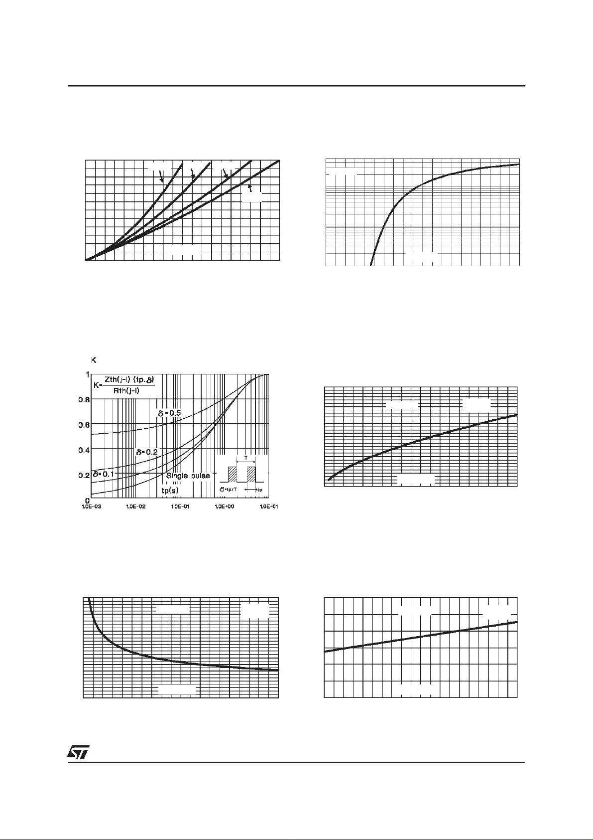
Fig.1: Conduction losses versus average current.
P1(W)
1.50
δ = 0.1
δ= 0.5δ = 0.2
1.25
1.00
δ =1
0.75
0.50
0.25
0.00
0.0 0.1 0.2 0.3 0.4 0.5 0.6 0.7 0.8 0.9 1.0
IF(av) (A)
Fig. 3: Relative variation of thermal transient im-
pedancejunctionto leadversuspulse duration.
Fig. 2: Forward voltage drop versus forward current(Maximumvalues).
IFM(A)
50.0
Tj=125°C
10.0
1.0
VFM(V)
0.1
0.0 0.5 1.0 1.5 2.0 2.5 3.0 3.5 4.0 4.5 5.0
Fig.4: Peakreverse recoverycurrentversusdIF/dt
(90%confidence).
IRM(A)
15.0
I
12.5
F=2*IF(av)
10.0
7.5
5.0
2.5
0.0
0 20 40 60 80 100 120 140 160 180 200
dIF/dt(A/µs)
VR=600V
Tj=125°C
Fig. 5: Reverse recovery time versus dIF/dt (90%
confidence).
trr(ns)
300
250
IF=2*IF(av)
200
150
100
50
0
0 20 40 60 80 100 120 140 160 180 200
dIF/dt(A/µs)
VR=600V
Tj=125°C
Fig.6: Softnessfactor (tb/ta)versusdIF/dt(Typical
values).
S factor
1.00
IF<2*IF(av)
0.80
0.60
0.40
0 20 40 60 80 100 120 140 160 180 200
dIF/dt(A/µs)
VR=600V
Tj=125°C
3/8
Page 4

STTA112U
Fig. 7: Relative variation of dynamic parameters
versusjunctiontemperature(ReferenceTj=125°C).
1.1
S factor
1.0
0.9
IRM
0.8
Tj(°C)
0.7
25 50 75 100 125
Fig. 9: Forward recovery time versus dIF/dt (90%
confidence).
tfr(ns)
800
700
IF=2*IF(av)
Tj=125°C
Fig. 8: Transient peak forward voltage versus
dI
/dt(90% confidence).
F
VFP(V)
80
70
IF=2*IF(av)
60
50
40
30
20
10
0
0 20406080100
dIF/dt(A/µs)
Tj=125°C
600
500
400
300
200
0 20406080100
VFR=1.1*VF max.
dIF/dt(A/µs)
4/8
Page 5

APPLICATION DATA
The 1200V TURBOSWITCH
designed to provide the lowest overall power
losses in all frequency or high pulsed current
operations.
TM
series has been
P = P1+ P2+P3+ P4+ P5 Watts
TOTALLOSSES
due to the diode
STTA112U
In such application (fig. A to D), the way of
calculatingthe power lossesis givenbelow :
CONDUCTION
LOSSES
inthe diode
Fig. A : ”FREEWHEEL MODE”.
SWITCHING
TRANSISTOR
V
R
tp
REVERSE
LOSSES
in the diode
T
SWITCHING
LOSSES
in the diode
DIODE:
TURBOSWITCH
SWITCHING
LOSSES
in the diode
due tothe diode
IL
F=1/T δ= tp/T
LOAD
5/8
Page 6

STTA112U
APPLICATION DATA (Cont’d)
Fig.B : SNUBBERDIODE. Fig. C : DEMAGNETIZINGDIODE.
PWM
tp
T
F=1/T δ= tp/T
Fig.D : RECTIFIERDIODE.
Fig. E : STATICCHARACTERISTICS.
I
I
F
Rd
V
R
to
V
F
6/8
V
I
R
Conductionlosses :
P1 = V
toxIF(AV)+RdxIF2(RMS)
Reverse losses:
P2 = V
V
RxIR x (1 -
)
δ
Page 7

APPLICATION DATA (Cont’d)
Fig.F : TURN-OFFCHARACTERISTICS.
V
IL
TRANSISTOR
I
STTA112U
Turn-onlosses:
(inthe transistor,due to the diode)
2
6
xdI
I
×(S+
L
d
IF
×(
F
⁄
3+2
⁄
dt
dt
2
×S)
)×
F
F
I
V
×
R
P5 =
V
R
t
+
RM
I
×
×
RM
2×
I
dI /dt
F
V
I
RM
tbta
dI /dt
R
DIODE
trr = ta + tb S = tb / ta
I
dIF/dt = VR/L
RECTIFIER
OPERATION
V
I
trr = ta + tb
S = tb/ta
RM
tbta
dI /dt
R
Fig.G : TURN-ON CHARACTERISTICS.
VR
V
Turn-offlosses :
V
R
P3=
t
2
I
×
RM
6
x
dI
××
F
⁄
S×F
dt
Turn-offlosses :
withnon negligibleserial inductance
V
P3’=
R
t
2
I
×
RM
6
xdI
×
⁄
F
S×F
dt
L×I
+
RM
2
2
F
×
P3, P3’ and P5 are suitable for power MOSFET
andIGBT
R
I
F
I
dI /dt
F
Fmax
Turn-onlosses:
P4= 0.4 (V
0
V
F
V
Fp
1.1V
F
0t
tfr
t
V
F
FP-VF
)xI
Fmaxxtfr
xF
7/8
Page 8

STTA112U
PACKAGEMECHANICAL DATA
SMB
E1
D
E
DIMENSIONS
REF.
Millimeters Inches
Min. Max. Min. Max.
A1 1.90 2.45 0.075 0.096
A2 0.05 0.20 0.002 0.008
b 1.95 2.20 0.077 0.087
c 0.15 0.41 0.006 0.016
A1
E 5.10 5.60 0.201 0.220
E1 4.05 4.60 0.159 0.181
C
L
A2
b
D 3.30 3.95 0.130 0.156
L 0.75 1.60 0.030 0.063
FOOTPRINTDIMENSIONS(inmillimeters)
2.3
1.52 2.75
1.52
Orderingtype Marking Package Weight Baseqty Deliverymode
STTA112U T03 SMB 0.107g 2500 Tape &reel
Epoxy meetsUL94,V0
Band indicatescathode
Informationfurnished is believedto be accurate and reliable.However, STMicroelectronics assumesno responsibilityfor the consequences of
use ofsuch information nor for any infringementof patents orother rights of thirdparties which may resultfrom its use.No license is granted by
implication or otherwise under any patent or patent rights of STMicroelectronics. Specifications mentioned in this publication are subject to
change withoutnotice. This publication supersedes and replaces all information previously supplied.
STMicroelectronics products are not authorized for use as critical components in lifesupportdevices or systems without express writtenapproval of STMicroelectronics.
The ST logo is a registeredtrademark of STMicroelectronics
1999 STMicroelectronics - Printed in Italy - All rights reserved.
STMicroelectronics GROUP OF COMPANIES
Australia - Brazil - China - Finland - France - Germany - Hong Kong - India - Italy - Japan - Malaysia
Malta - Morocco - Singapore -Spain - Sweden - Switzerland - United Kingdom - U.S.A.
http://www.st.com
8/8
 Loading...