

Page 1
®
TURBOSWITCH ULTRA-FAST HIGH VOLTAGE DIODE
MAIN PRODUCT CHARACTERISTIC S
STTA106/U
I
F(AV)
V
RRM
t
(typ) 20ns
rr
V
(max) 1.5V
F
1A
600V
FEATURES AND BENEFITS
SPECIFIC TO FREEWHEEL MODE
OPERATIONS : FREEWHEEL OR BOOSTER
DIODE
ULTRA-FAST AND SOFT RECOVERY
VERY LOW OVERALL POWER LOSSES IN
BOTH THE DIODE AND THE COMPANION
TRANSISTOR
HIGH FREQUENCY OPERATIONS
DESCRIPTION
The TURBOSWITCH is a very high performance
series of ultra-fast high voltage power diodes.
TURBOSWITCH family drastically cuts losses in
both the diode and the associated switching IGBT
and MOSFET in all freewheel mode operations
and is particulary suitable and efficient in motor
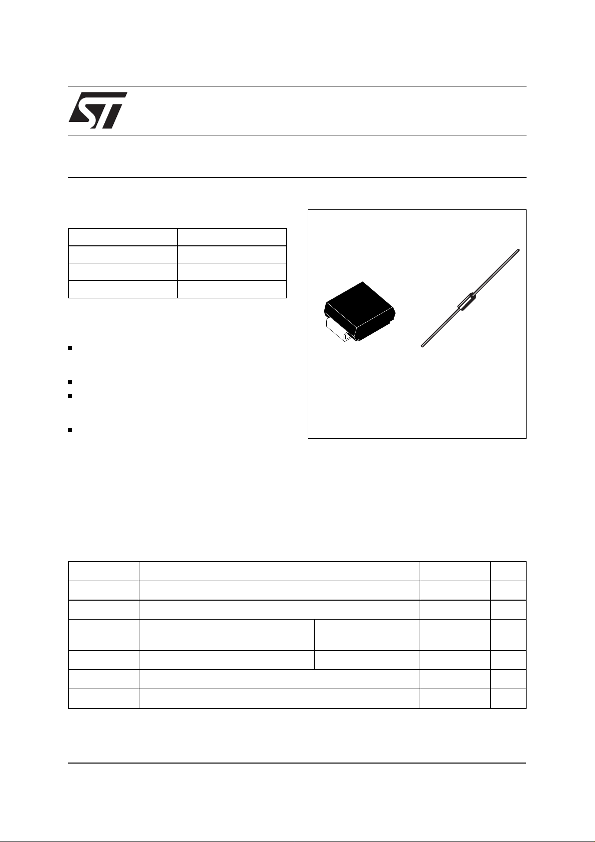
SMB
STTA106U
F126
STTA106
control freewheel applications and in booster diode
applications in power factor control circuitries.
Available either in SMB or F126 axial package,
these 600V devices are particularly intended for
use on 240V domestic mains.
ABSOLUTE RATINGS (limiting values)
Symbol Parameter Value Unit
V
RRM
I
F(RMS)
I
FRM
Repetitive peak reverse voltage 600 V
RMS forward current 6 A
Repetitive peak forward current tp = 5 µs
10 A
F = 5kHz s quare
I
FSM
T
j
T
stg
TM : TURBOSWITCH is a trademark of STMicroelectronics
November 1999 - Ed: 5C
Surge non repetitive forward current tp = 10 ms sinusoidal 25 A
Maximum operating junction temperature 125 ° C
Storage temperature range - 65 to + 150 ° C
1/8
Page 2
STTA106/U
THERMAL AND P OW ER DATA
Symbol Parameter Test conditions Value Unit
R
th(j-I)
P
1
P
max
STATIC ELECTRICAL CHARACTE RISTICS
Symbol Parameter Test conditions Min Typ Max Unit
V
F *
I
R **
V
to
Rd Dynamic resistance 350 m
Test pulse : * tp = 380 µs, δ < 2%
Junction to lead SMB 23 °C/W
Junction to lead L=5mm F126 45 ° C/W
Conduction power
dissipation
I
= 0.8A δ = 0.5
F(AV)
Tlead= 93°C
I
= 0.8A δ = 0.5
F(AV)
SMB 1.4 W
F126 1.4 W
Tlead= 60°C
Total power dissipation
Pmax = P1 + P3
Tlead= 90°C SMB 1.5 W
Tlead= 60°C F126 1.5 W
(P3 = 10% P1)
Forward voltage drop IF = 1A Tj = 25°C
Reve rse le akag e curre nt VR = 0.8 x
Threshold voltage Ip < 3.I
** tp = 5 ms, δ < 2%
V
RRM
F(AV)
Tj = 125°C
Tj = 25°C
Tj = 125°C 25010750
Tj = 125°C 1.15 V
1.1
1.75
1.5
V
A
µ
Ω
To evaluate the maximum conduction losses use the following equation :
P = V
x I
to
F(AV)
+ Rd x I
F2(RMS)
DYNAMIC ELECTRICAL CHARACTE RISTICS
TURN-OFF SWITCHING
Symbol Parameter Test conditions Min Typ Max Unit
t
rr
Reverse
recover y time
I
RM
Maximum
recover y curre nt
S factor Softness factor Tj = 125°C V
Tj = 25°C
I
= 0.5 A IR = 1A Irr = 0.25A
F
I
= 1 A dIF/dt =-50A/µs VR = 30V
F
20
50
Tj = 125°C VR = 400V IF = 1A
dI
/dt = -8 A/µs
F
dI
/dt = -50 A/µs1.6
F
= 400V IF =1A
R
dI
/dt = -50 A/µs1.1
F
0.6
TURN-ON SWITCHING
Symbol Parameter Test conditions Min Typ Max Unit
t
fr
Forward
recove ry time
V
Fp
Peak forward
Tj = 25°C
I
= 1 A, dIF/dt = 8 A/µs
F
measured at 1.1
×
VF max
500 ns
10 V
voltage
ns
A
/
2/8
Page 3
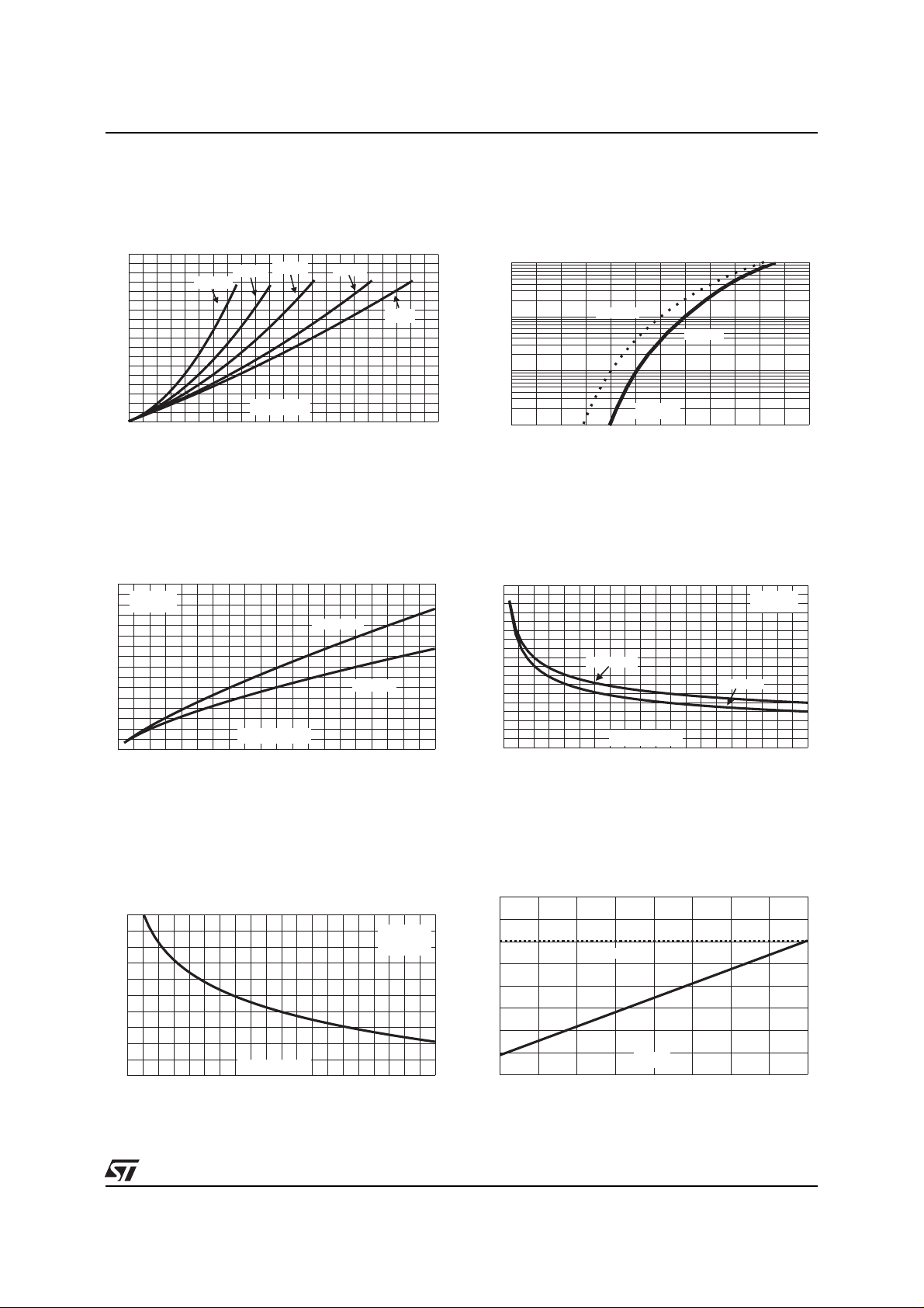
: Conduction losses versus average current.
Fig. 1
Forward voltage drop versus forward cur-
Fig. 2:
rent (maximum values).
STTA106/U
P1(W)
1.8
1.6
1.4
1.2
δ = 0.05
δ = 0.1
δ = 0.2
δ = 0.5
δ = 1
1.0
0.8
0.6
0.4
0.2
0.0
0.0 0.1 0.2 0.3 0.4 0.5 0.6 0.7 0.8 0.9 1.0 1.1
Peak re verse r ecovery current v ersus dI
Fig. 3:
IF(av) (A)
(90% confidence).
IRM(A)
8
VR=400V
7
Tj=125°C
6
5
4
3
2
1
0
0 50 100 150 200
dIF/dt(A/µs)
IF=2*IF(av)
IF=IF(av)
IFM(A)
1E+1
1E+0
1E-1
1E-2
0.0 0.5 1.0 1.5 2.0 2.5 3.0
/dt
F
Reverse recovery time versus dI
Fig. 4:
Tj=125°C
VFM(V)
Tj=25°C
/dt (90%
F
confidence).
trr(ns)
225
200
175
150
125
100
75
50
25
0
0 20 40 60 80 100 120 140 160 180 200
IF=2*IF(av)
dIF/dt(A/µs)
IF=IF(av)
VR=400V
Tj=125°C
Softness factor (tb/ta) versus dI
Fig. 5:
/dt (typical
F
values).
S factor
1.6
1.4
1.2
1.0
0.8
0.6
0 102030405060708090100
dIF/dt(A/µs)
IF=2*IF(av)
VR=400V
Tj=125°C
Fig. 6:
Relative variation of dynamic parameters
vers us junction te m pe r ature ( r eference Tj = 125°C).
1.1
1.0
0.9
0.8
0.7
25 50 75 100 125
S factor
IRM
Tj(°C)
3/8
Page 4

STTA106/U
Fig. 7:
dI
40
35
30
25
20
15
10
Fig. 9:
Transient peak forward voltage versus
/dt (90% confidence).
F
VFP(V)
IF=2A
Tj=125°C
5
0
0 20 40 60 80 100 120 140 160 180 200
dIF/dt(A/µs)
Junction capacitance versus reverse volt-
age applied (typical values).
C(pF)
10
F=1MHz
Forwa rd rec ov e ry t i me v ers us dI
Fig. 8:
/dt (90%
F
confidence).
tfr(ns)
550
500
450
400
350
300
250
200
150
100
50
0
0 20 40 60 80 100 120 140 160 180 200
dIF/dt(A/µs)
IF=2A
VFR=1.1*VF max.
Tj=125°C
5
2
VR(V)
1
1 10 100 200
4/8
Page 5

APPLICATION DATA
The TURBOSWITCH
provide the lowest overall power losses in any
"Freewhell Mode" application (see fig. A)
considering both diode and companion transistor,
thus optimizing the overall performance in the end
application.
TM
is especially designed to
P = P1+ P2+ P3+ P4+ P5 Watts
TOTAL LOSSES
due to the diode
STTA106/U
The way of calculating the power losses is given
below :
Fig. A :
CONDUCTION
LOSSES
in the diode
"FREEWHEEL" MODE
SWITCHING
TRANSISTOR
V
R
tp
REVERSE
LOSSES
in the diode
SWITCHING
LOSSES
in the diode
SWITCHING
LOSSES
in the transistor
due to the diode
IL
DIODE:
TURBOSWITCH
T
F=1/T δ= tp/T
LOAD
5/8
Page 6

STTA106/U
APPLICATION DATA (Cont’d)
Fig. B :
Fig. C :
STATIC CHARACTERISTICS
I
I
F
Rd
V
R
to
V
F
V
I
R
TURN-OFF CHARACTERIS TICS
V
TRANSISTOR
I
IL
x I
to
F(AV)
losses :
x I
R
R x (1 -
losses :
losses :
+ Rd x I
)
δ
F2(RMS)
Conduction
P1 = V
V
Reverse
P2 = V
Turn-on
(in the transistor, due to the diode)
I
RM
I
2
RM
6 x
×
×
2
× (3+2 ×
dI
⁄
F
×
I
S
(
L
dI
dt
⁄
F
×
V
R
P5 =
t
+
×
V
R
S
dt
+ 2) ×
F
)
×
F
I
dI /dt
V
I
RM
I
V
trr = ta + tb
S=tb/ta
F
DIODE
tbta
dI /dt
R
trr = ta + tb S = tb / ta
dI /dt
R
RECTIFIER
OPERATION
dIF/dt = VR/L
tbta
I
RM
VR
V
t
Turn-off
t
losses (in t he diode) :
P3 =
×
V
R
I
6 x
RM
dI
2
F
× S ×
dt
⁄
F
P3 and P5 are suitable for power MOSFET and
R
IGBT
6/8
Page 7

APPLICATION DATA (Cont’d)
STTA106/U
Fig. D :
TURN-ON CHARACTERIST ICS
I
F
dI /dt
F
0
V
F
V
Fp
1.1V
F
0t
tfr
PACKAGE MECHANICAL DATA
SMB
E1
I
Fmax
Turn-on
P4
t
V
F
D
losses :
= 0.4 (VFP - VF) x I
Fmax
x t
x F
fr
DIMENSIONS
REF.
Millimeters Inches
Min. Max. Min. Max.
A1 1.90 2.45 0.075 0.096
E
C
L
FOOTPRINT DIMENSIONS
1.52 2.75
A1
A2
(in millimeters)
2.3
1.52
A2 0.05 0.20 0.002 0.008
b 1.95 2.20 0.077 0.087
c 0.15 0.41 0.006 0.016
E 5.10 5.60 0.201 0.220
E1 4.05 4.60 0.159 0.181
D 3.30 3.95 0.130 0.156
b
L 0.75 1.60 0.030 0.063
7/8
Page 8

STTA106/U
PACKAGE MECHANICAL DATA
F126
A
CC
REF.
Millimeters Inches
DIMENSIONS
Min. Typ. Max. Min. Typ. Max.
A 6.05 6.20 6.35 0.2380.244 0.250
D
B
D
B 2.95 3.00 3.05 0.1160.118 0.120
C 26 31 1.024 1.220
D 0.76 0.81 0.86 0.030 0.032 0.034
MARKING
Type Marking Package Weight Base Qty Delivery mode
STTA106U T01 SMB 0.11g 2500 tape & reel
STTA106 STTA106 F126 0.39g 1000 box
STTA106RL STTA106 F126 0.39g 6000 tape & reel
Band indicates cathode
Epoxy meets UL94,V0
Information furnished is believed to be accurate and reliable. However, STMicroelectronics assumes no responsibility for the consequences of
use of such information nor for any infringement of patents or other rights of third parties which may result from its use. No license is granted by
implication or otherwis e under any patent or patent rights of STMicroelec tronics. Specificati ons mentioned in this publication are subject to
change without notice. This publication supersedes and replaces all information previously supplied.
STMicroelectronics products ar e not authorized for use as critical c om ponents in life support devi ces or systems without ex press written approval of STMicroelectronics.
The ST logo is a registered trademark of S TMicroelectron ics
© 1999 STMicroelectronics - Printed in Italy - All rights reserved.
STMicroelectronics GROUP OF COMPANIES
Australia - Brazil - China - Finland - France - Germany - Hong Kong - India - Italy - Japan - Malaysia
Malta - Morocco - Singapore - Spain - Sweden - Switzerland - United Kingdom - U.S.A.
http://www.st.com
8/8
 Loading...