

Page 1
STT5NF20V
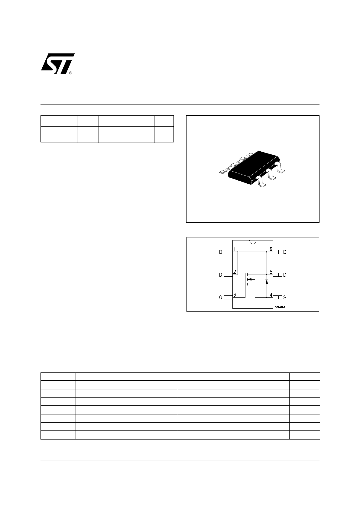
N-CHANNEL 20V - 0.030 Ω - 5A SOT23-6L
2.7V-DRIVE STripFET™ II POWER MOSFET
TYPE
V
DSS
STT5NF20V 20 V
■ TYPICAL R
■ TYPICAL R
■ ULTRA LOW THRESHOLD
(on) = 0.030 Ω @ 4.5 V
DS
(on) = 0.037 Ω @ 2.7 V
DS
R
DS(on)
< 0.040 Ω ( @ 4.5 V )
< 0.045 Ω ( @ 2.7 V )
I
D
5 A
GATE DRIVE (2.7 V)
■ STANDARD OUTLI NE FO R EASY
AUTOMATED SURFACE MOUNT ASSEMBLY
DESCRIPTION
This Power MOSFET is the latest dev elo pment of
STMicroelectronis unique "Single Feature Size™"
strip-based process. The resulting transistor
shows extremely high packing density for low onresistance, rugged avalanche characteristics and
less critical alignment steps therefore a remarkable manufacturing reproducibility.
APPLICATIONS
■ DC MOTOR DRIVE
■ DC-DC CONVERTERS
■ BATTERY MANAGEMENT IN NOMADIC
EQUIPMENT
■ POWER MANAGEMENT IN
PORTABLE/DESKTOP PCs
SOT23-6L
INTERNAL SCHEMATIC DIAGRAM
ABSOLUTE MAXIMUM RATINGS
Symbol Parameter Value Unit
V
DS
V
DGR
V
GS
I
D
I
D
(
I
DM
P
tot
(
Pulse widt h l i m i ted by safe operating area .
•)
.
Drain-source Voltage (VGS = 0)
Drain-gate Voltage (RGS = 20 kΩ)
20 V
20 V
Gate- source Voltage ± 12 V
Drain Current (continuous) at TC = 25°C
Drain Current (continuous) at TC = 100°C
•)
Drain Current (pulsed) 20 A
Total Dissipation at TC = 25°C
5A
3A
1.6 W
1/8May 2002
Page 2
STT5NF20V
THERMA L D ATA
Rthj-amb
T
T
stg
Thermal Resistance Junction-ambient
Max. Operating Junction Temperature
j
Storage Temperature
Max 78
-55 to 150
-55 to 150
°C/W
°C
°C
ELECTRICAL CHARACTERISTICS (T
= 25 °C unless otherwise specified)
case
OFF
Symbol Parameter Test Conditions Min. Typ. Max. Unit
I
V
(BR)DSS
Drain-source
= 250 µA, VGS = 0
D
20
Breakdown Voltage
V
= Max Rating
DS
V
= Max Rating TC = 125°C
DS
V
= ± 12V
GS
1
10
±100 nA
ON
(*)
I
DSS
I
GSS
Zero Gate Voltage
Drain Current (V
GS
Gate-body Leakage
Current (V
DS
= 0)
= 0)
Symbol Parameter Test Conditions Min. Typ. Max. Unit
V
V
GS(th)
R
DS(on)
Gate Threshold Voltage
Static Drain-source On
Resistance
= VGS ID = 250 µA
DS
= 4.5 V ID = 2.5 A
V
GS
V
= 2.7 V ID = 2.5 A
GS
0.6 V
0.030
0.037
0.040
0.045
DYNAMIC
Symbol Parameter Test Conditions Min. Typ. Max. Unit
(*)
g
fs
C
iss
C
oss
C
rss
Forward Transconductance
Input Capacitance
Output Capacitance
Reverse Transfer
Capacitance
V
=15 V ID= 2.5 A
DS
= 15V f = 1 MHz, VGS = 0
V
DS
9.5 S
460
200
50
V
µA
µA
Ω
Ω
pF
pF
pF
2/8
Page 3
STT5NF20V
ELECTRICAL CHARACTERISTICS (continued)
SWITCHING ON
Symbol Parameter Test Conditions Min. Typ. Max. Unit
= 10 V ID = 2.5 A
t
d(on)
Turn-on Delay Time
t
r
Rise Time
V
DD
R
= 4.7 Ω VGS = 4.5 V
G
(Resistive Load, Figure 1)
Q
g
Q
gs
Q
gd
Total Gate Charge
Gate-Source Charge
Gate-Drain Charge
= 16V ID= 5A VGS=4.5V
V
DD
(see test circuit, Figure 2)
SWITCHING OFF
Symbol Parameter Test Conditions Min. Typ. Max. Unit
= 10 V ID = 2.5 A
t
d(off)
Turn-off Delay Time
t
f
Fall Time
V
DD
R
= 4.7Ω, V
G
GS
= 4.5 V
(Resistive Load, Figure 1)
7
33
8.5
1.8
2.4
27
10
11.5 nC
ns
ns
nC
nC
ns
ns
t
d(Voff)
t
t
c
Off-voltage Rise Time
f
Fall Time
Cross-over Time
= 16 V ID = 5 A
V
clamp
R
= 4.7Ω, V
G
GS
(Inductive Load, Figure 3)
= 4.5 V
26
11
21
SOURCE DRAIN DIODE
Symbol Parameter Test Conditions Min. Typ. Max. Unit
I
SD
I
SDM
V
SD
t
rr
Q
rr
I
RRM
(*)
Pulsed: P ul se duration = 300 µs, duty cycle 1. 5 %.
(
•)Pulse width limited by saf e operating area.
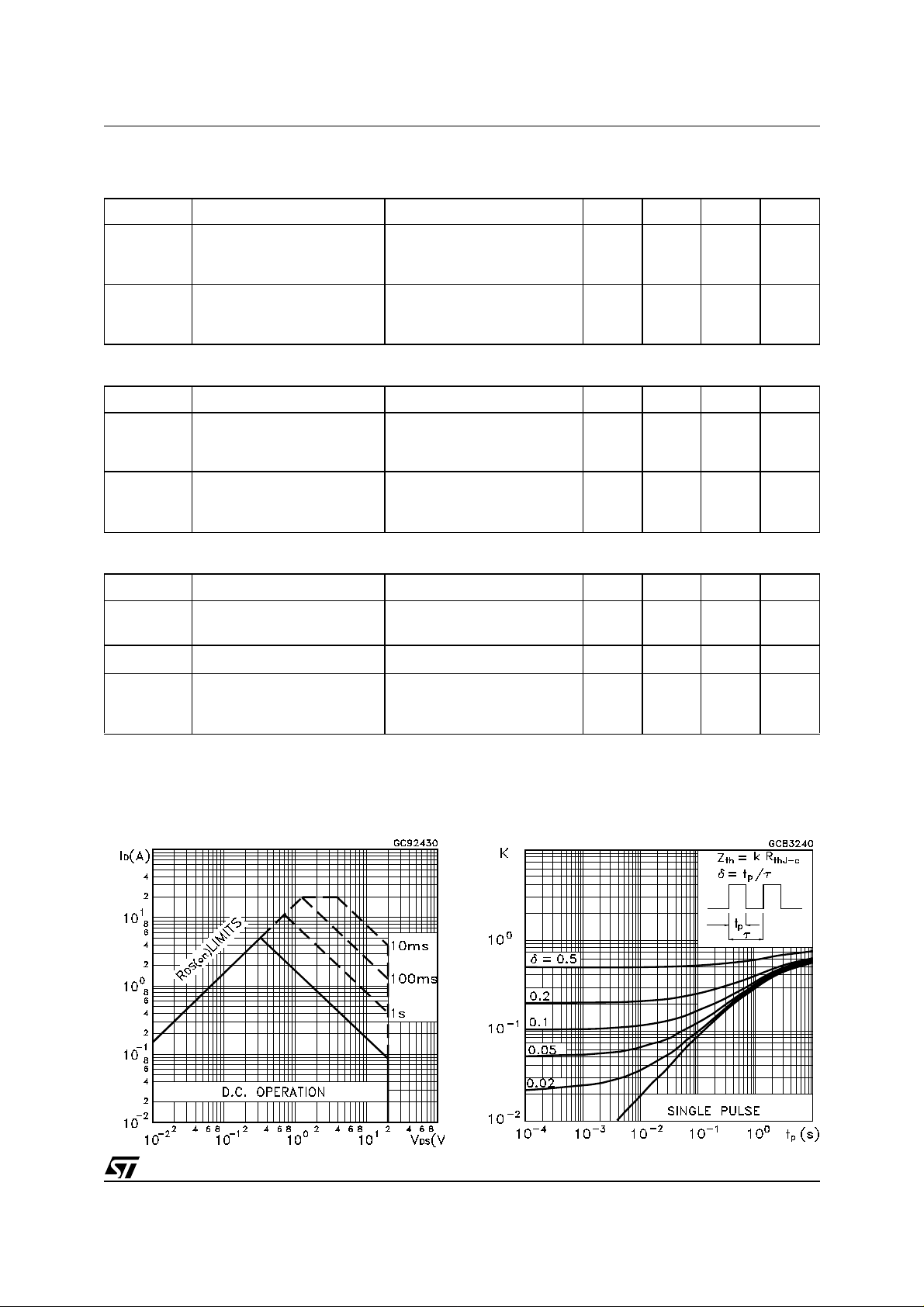
Safe Operating Area
Source-drain Current
(•)
Source-drain Current (pulsed)
(*)
Forward On Voltage
Reverse Recovery Time
Reverse Recovery Charge
Reverse Recovery Current
I
= 5 A VGS = 0
SD
= 5 A di/dt = 100A/µs
I
SD
V
= 10 V Tj = 150°C
DD
(see test circuit, Figure 3)
Thermal Impedance
5
20
1.2 V
26
13
1
ns
ns
ns
A
A
ns
nC
A
3/8
Page 4

STT5NF20V
Output Characteristics Transfer Characteristics
Transconductance Static Drain-source On Resistance
Gate Charge vs Gate-source Voltage Capacitance Variations
4/8
Page 5

Normalized Gate Threshold Voltage vs Temperature Normalized on Resistance vs Temperature
Source-drain Diode Forward Characteristics .
STT5NF20V
. .
5/8
Page 6

STT5NF20V
Fig. 1: Switching Times Test Circuits For Resistive
Load
Fig. 3: Test Circuit For Diode Recovery Behaviour
Fig. 2: Gate Charge test Circuit
6/8
Page 7

SOT23-6L MECHANICAL DATA
STT5NF20V
DIM.
MIN. TYP. MAX. MIN. TYP. MAX.
A 0.90 1.45 0.035 0.057
A1 0.00 0.15 0.000 0.006
A2 0.90 1.30 0.035 0.051
b 0.25 0.50 0.010 0.020
C 0.09 0.20 0.004 0.008
D 2.80 3.10 0.110 0.122
E 2.60 3.00 0.102 0.118
E1 1.50 1.75 0.059 0.069
L 0.35 0.55 0.014 0.022
e 0.95 0.037
e1 1.90 0.075
mm mils
AA2
A1
b
e
c
L
E
e1
D
E1
7/8
Page 8

STT5NF20V
Information furnished is believed to be accurate and reliable. However, STMicroelectronics assumes no responsibility for the consequences
of use of such information nor for any infringement of patents or other rights of third parties which may result from its use. No license is granted
by implic ation or oth erwise unde r any patent or patent r i ghts of STMi croelectronics. Speci fications mentioned in this publication are subject
to change without notice. This publication supersedes and replaces all information previously supplied. STMicroelectronics products are not
authorized for use as crit i cal components in life suppo rt devices or sy st em s without express written approval of STM i croelectronics.
The ST logo is registered trademark of STMicroelectronics
2002 STMi croelectroni cs - All Rights Reserved
All other na m es are the property of their res pective owners.
Australi a - Brazil - Cana da - China - Finl and - France - Germany - Hong Kong - India - Israel - Italy - Ja pan - Malaysi a - M al ta - Morocco -
Singap ore - Spain - Sw eden - Switzerl and - United Ki ngdom - United States.
STMicroelectronics GROUP OF COMPANIES
http:// www.st.com
8/8
 Loading...