

Page 1
N - CHANNEL 30V - 0.055Ω - 4A - TSOP-6
TYPE V
ST T 4NF30L 30 V < 0.065 Ω 4A
■ TYPICALR
■ STANDARD OUTLINE FOR EASY
DS(on)
DSS
= 0.055 Ω
AUTOMATEDSURFACEMOUNTASSEMBLY
■ LOW THRESHOLDDRIVE
DESCRIPTION
This Power MOSFET is the latest developmentof
STMicroelectronics unique ”Single Feature
Size” strip-based process.The resulting transi-
stor shows extremelyhigh packing density forlow
on-resistance, rugged avalanche characteristics
and less critical alignment steps therefore a remarkablemanufacturingreproducibility.
APPLICATIONS
■ DC MOTOR DRIVE
■ DC-DCCONVERTERS
■ BATTERYMANAGEMENTIN NOMADIC
EQUIPMENT
■ POWERMANAGEMENT IN
PORTABLE/DESKTOPPCs
R
DS(on)
I
D
STT4NF30L
STripFET MOSFET
PRELIMINARY DATA
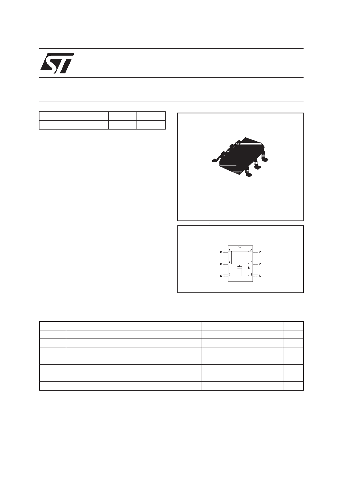
TSOP-6
INTERNAL SCHEMATIC DIAGRAM
ABSOLUTE MAXIMUM RATINGS
Symbol Parameter Value Unit
V
V
V
I
DM
P
(•) Pulsewidth limited by safe operating area
November 1998
Dra in- sour c e Vol t age ( VGS=0) 30 V
DS
Dra in- gate Volt age (RGS=20kΩ)30V
DGR
Gat e-sourc e Voltage
GS
I
Dra in C u rr ent (c ont in uous) at Tc=25oC4A
D
I
Dra in C u rr ent (c ont in uous) at Tc=100oC2.5A
D
(•) D rain Curr ent (p ulsed ) 16 A
Tot al Dissipation at Tc=25oC2W
tot
20 V
±
1/5
Page 2
STT4NF30L
THERMAL DATA
R
thj-amb
T
T
(*)Mounted on FR-4 board (t ≤ 5 sec)
(*)T hermal Resistance Junction-ambie nt Max
Maximum O per ating Junct io n Tempe rat ur e
J
Sto rage Temperatur e
stg
62.5
150
-55 to 150
o
C/W
o
o
C
C
ELECTRICAL CHARACTERISTICS
=25oC unless otherwisespecified)
(T
case
OFF
Symbol Parameter Test Conditions Min. Typ. Max. Unit
V
(BR)DSS
Drain-source
ID=250µAVGS=0 30 V
Break dow n V o lt age
ON (
I
DSS
I
GSS
∗)
Zero Gate Voltage
Drain Cur re nt ( V
GS
Gat e- bod y L eakage
Current (V
DS
=0)
=0)
V
=MaxRating
DS
=MaxRating Tc= 125oC
V
DS
= ± 20 V ± 100 nA
V
GS
1
10
Symbol Parameter Test Conditions Min. Typ. Max. Unit
V
GS(th)
R
DS(on)
I
D(on)
Gate Threshold Voltage VDS=VGSID= 250 µA11.72.5V
Sta t ic Drain -s ource On
Resistance
VGS=10V ID=2A
=4.5V ID=2A
V
GS
On State Drain Current VDS>I
D(on)xRDS(on)max
0.055
0.06
4A
0.065
0.09
VGS=10V
DYNAMIC
Symbol Parameter Test Conditions Min. Typ. Max. Unit
g
(∗)Forward
fs
Tr ansc on duc tance
C
C
C
Input Capac i t ance
iss
Out put Capacitance
oss
Reverse Tr ansfer
rss
Capacit a nc e
VDS>I
D(on)xRDS(on)maxID
=6 A 6 S
VDS=25V f=1MHz VGS= 0 420
62
20
550
80
30
µA
µA
Ω
Ω
pF
pF
pF
2/5
Page 3

STT4NF30L
ELECTRICAL CHARACTERISTICS
(continued)
SWITCHINGON
Symbol Parameter Test Conditions Min. Typ. Max. Unit
t
d(on)
t
r
Turn-on Time
Rise Ti me
VDD=15V ID=2A
R
G
=4.7
Ω
VGS=4.5V
13
30
17
40
(see test circuit, figure 3)
Q
Q
Q
Tot al Gat e Charge
g
Gat e- Source Charge
gs
Gate-Drain Charge
gd
VDD=24V ID=4A VGS=4.5V 8
3.2
2.6
12 nC
SWITCHING OFF
Symbol Parameter Test Conditions Min. Typ. Max. Unit
t
r(Voff)
t
t
Off-voltage Rise T ime
Fall T ime
f
Cross-over Tim e
c
VDD=24V ID=4A
=4.7 Ω VGS=4.5V
R
G
(see test circuit, figure 5)
20
6
9
8
12
26
SOURCEDRAIN DIODE
Symbol Parameter Test Conditions Min. Typ. Max. Unit
I
SD
I
SDM
V
SD
t
Q
I
RRM
(∗) Pulsed:Pulse duration= 300µs, duty cycle 1.5%
(•) Pulse width limited by safe operatingarea
Source-drain Current
(•)
Source-drain Current
4
16
(pulsed)
(∗)ForwardOnVoltage ISD=4A VGS=0 1.2 V
Reverse Recovery
rr
Time
Reverse Recovery
rr
ISD= 4 A di/dt = 100 A/µs
=15V Tj= 150oC
V
DD
(see test circuit, figure 5)
22
13
Charge
Reverse Recovery
1.2
Current
ns
ns
nC
nC
ns
ns
ns
A
A
ns
nC
A
3/5
Page 4

STT4NF30L
Fig. 1: Unclamped Inductive Load Test Circuit
Fig. 3: Switching Times Test Circuits For
ResistiveLoad
Fig. 2: Unclamped InductiveWaveform
Fig. 4: Gate Chargetest Circuit
Fig. 5: Test Circuit For InductiveLoad Switching
And Diode Recovery Times
4/5
Page 5

STT4NF30L
Information furnished is believed to be accurate and reliable. However, STMicroelectronics assumes no responsibility forthe consequences
of use of such information nor for any infringement of patents or other rights of third parties which may result from its use. No license is
granted by implication or otherwise under any patent or patent rights of STMicroelectronics. Specification mentioned in this publication are
subject to change without notice. This publication supersedes and replaces all information previously supplied. STMicroelectronics products
are not authorized for use as critical components in life support devices or systems without express written approval of STMicroelectronics.
The ST logo is a trademarkof STMicroelectronics
1998 STMicroelectronics – Printed in Italy – All Rights Reserved
STMicroelectronics GROUP OF COMPANIES
Australia - Brazil - Canada -China - France -Germany - Italy - Japan -Korea - Malaysia -Malta - Mexico -Morocco - The Netherlands -
Singapore - Spain - Sweden - Switzerland - Taiwan - Thailand - United Kingdom - U.S.A.
http://www.st.com
.
5/5
 Loading...