

Page 1
Features
V
DSS
100 V 6 A 0.30 Ω 22 nC
■ Fast switching
■ 100% avalanche tested
■ Hermetic package
■ 70 krad TID
■ SEE radiation hardened
I
D
R
DS(on)
Applications
■ Satellite
■ High reliability
STRH8N10
Rad-Hard N-channel 100 V, 6 A
Power MOSFET
Q
g
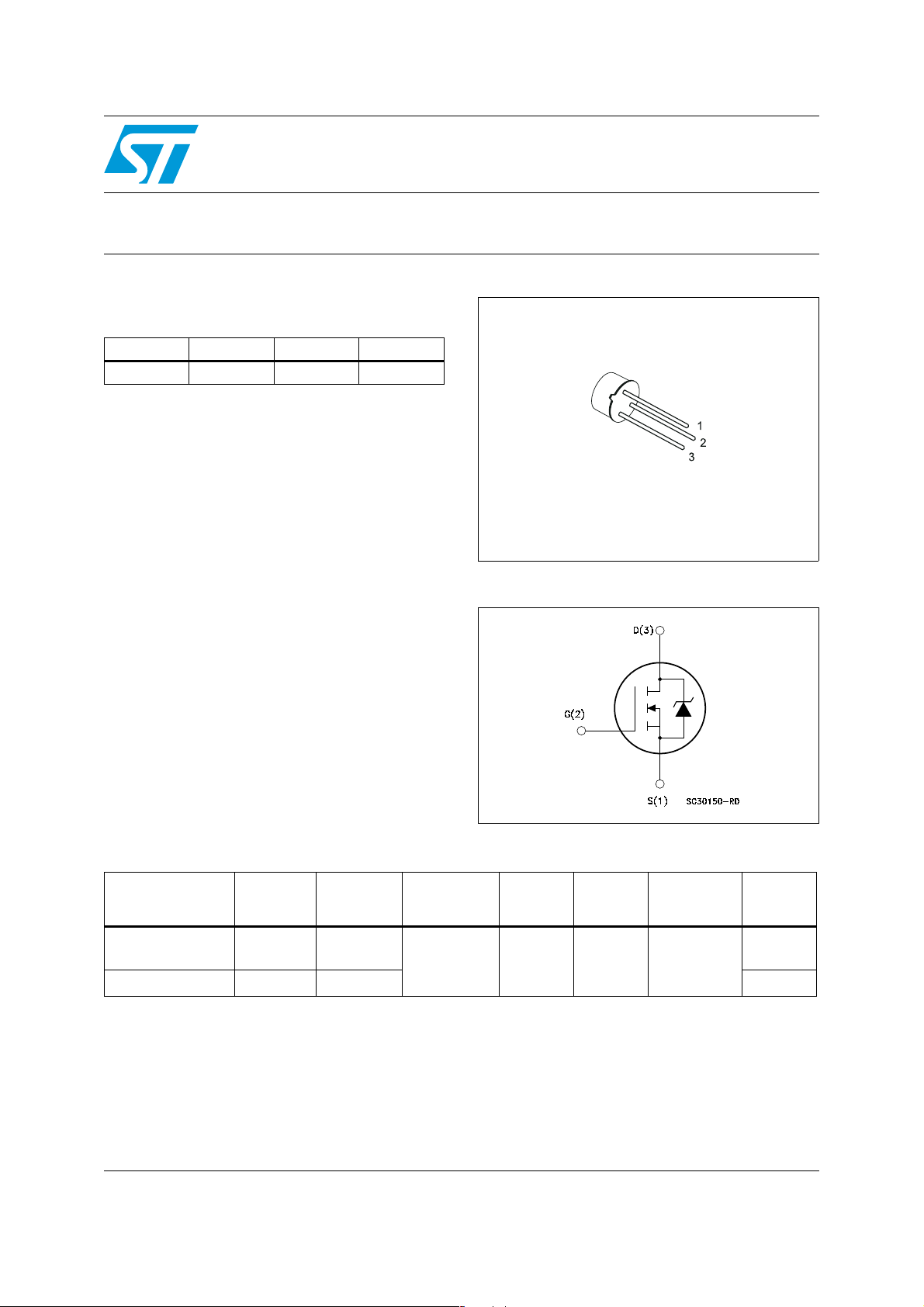
TO-39
Figure 1. Internal schematic diagram
Description
This N-channel Power MOSFET is developed with
STMicroelectronics unique STripFET
has specifically been designed to sustain high
TID and provide immunity to heavy ion effects.
Table 1. Device summary
Order code
STRH8N10N1 -
STRH8N10NG TBD ESCC flight Target
ESCC part
number
Note: Contact ST sales office for information about the specific conditions for product in die form
and for other packages.
™
process. It
Quality
level
Engineering
model
Package
TO-39 Gold 1.2 -55 to 150°C
Lead
finish
Mass
(g)
Temp. range EPPL
-
November 2011 Doc ID 010029 Rev 2 1/18
www.st.com
18
Page 2

Contents STRH8N10
Contents
1 Electrical ratings . . . . . . . . . . . . . . . . . . . . . . . . . . . . . . . . . . . . . . . . . . . . 3
2 Electrical characteristics . . . . . . . . . . . . . . . . . . . . . . . . . . . . . . . . . . . . . 5
2.1 Pre-irradiation . . . . . . . . . . . . . . . . . . . . . . . . . . . . . . . . . . . . . . . . . . . . . . . 5
3 Radiation characteristics . . . . . . . . . . . . . . . . . . . . . . . . . . . . . . . . . . . . . 7
4 Electrical characteristics (curves) . . . . . . . . . . . . . . . . . . . . . . . . . . . . . 10
5 Test circuit . . . . . . . . . . . . . . . . . . . . . . . . . . . . . . . . . . . . . . . . . . . . . . . . 12
6 Package mechanical data . . . . . . . . . . . . . . . . . . . . . . . . . . . . . . . . . . . . 14
7 Order codes . . . . . . . . . . . . . . . . . . . . . . . . . . . . . . . . . . . . . . . . . . . . . . . 16
8 Revision history . . . . . . . . . . . . . . . . . . . . . . . . . . . . . . . . . . . . . . . . . . . 17
2/18 Doc ID 010029 Rev 2
Page 3
STRH8N10 Electrical ratings
1 Electrical ratings
(TC = 25°C unless otherwise specified)
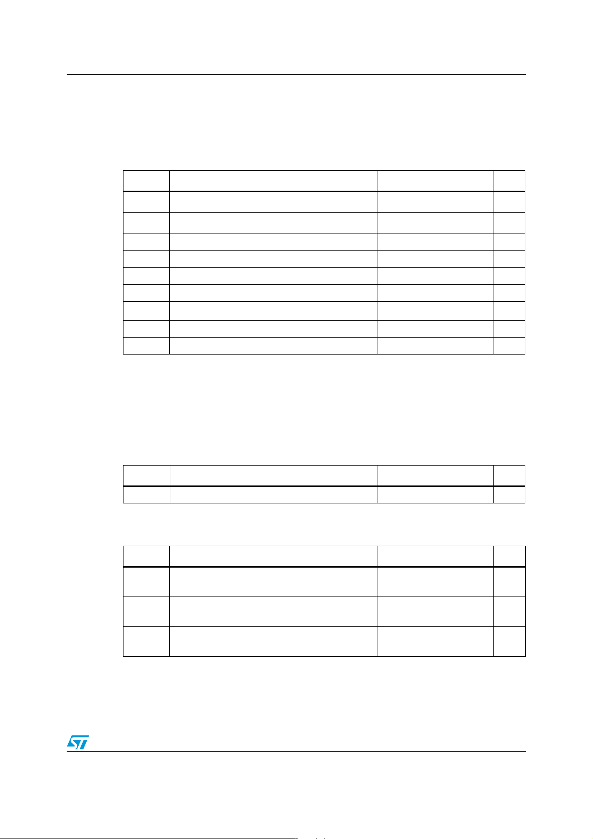
Table 2. Absolute maximum ratings (pre-irradiation)
Symbol Parameter Value Unit
(1)
V
DS
V
GS
I
D
I
D
I
DM
P
TOT
dv/dt
T
1. This rating is guaranteed @ TJ > 25 °C (see Figure 10: Normalized BV
2. This value is guaranteed over the full range of temperature.
3. Rated according to the Rthj-case + Rthc-s.
4. Pulse width limited by safe operating area.
5. ISD ≤ 6 A, di/dt ≤ 1060 A/µs, VDD = 80% V
Drain-source voltage (VGS = 0)
(2)
Gate-source voltage ±20 V
(3)
Drain current (continuous) at TC= 25°C 6 A
(1)
Drain current (continuous) at TC= 100°C 4.1 A
(4)
Drain current (pulsed) 24 A
(1)
Total dissipation at TC= 25°C 25 W
(5)
Peak diode recovery voltage slope 6.4 V/ns
Storage temperature -55 to 150 °C
stg
T
Max. operating junction temperature 150 °C
j
(BR)DSS
DSS
100 V
vs temperature).
Table 3. Thermal data
Symbol Parameter Value Unit
Rthj-case Thermal resistance junction-case 5.0 °C/W
Table 4. Avalanche characteristics
Symbol Parameter Value Unit
I
E
AS
E
Avalanche current, repetitive or not-repetitive
AR
(pulse width limited by Tj Max)
Single pulse avalanche energy
(1)
(starting Tj=25°C, Id=Iar, Vdd=50V)
Single pulse avalanche energy
AS
(starting Tj=110°C, Id=Iar, Vdd=50V)
4A
457 mJ
134 mJ
Doc ID 010029 Rev 2 3/18
Page 4

Electrical ratings STRH8N10
Table 4. Avalanche characteristics (continued)
Symbol Parameter Value Unit
Repetitive avalanche
E
AR
(Vdd = 50 V, I
duty cycle = 10%)
Repetitive avalanche
E
(Vdd = 50 V, IAR = 4 A, f = 100 KHz, TJ = 110 °C,
AR
duty cycle = 10%)
1. Maximum rating value.
= 4 A, f = 100 KHz, TJ = 25 °C,
AR
4.3 mJ
1.4 mJ
4/18 Doc ID 010029 Rev 2
Page 5
STRH8N10 Electrical characteristics
2 Electrical characteristics
(T
= 25°C unless otherwise specified).
CASE
2.1 Pre-irradiation
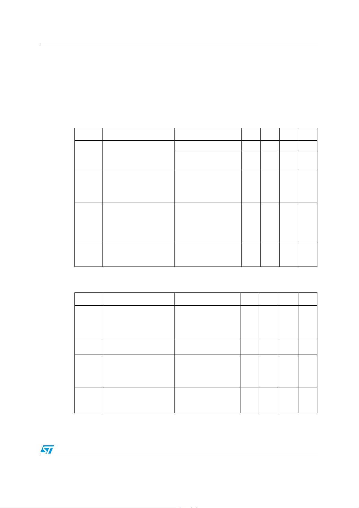
Table 5. On/off states
Symbol Parameter Test conditions Min. Typ. Max. Unit
I
I
V
GS(th)
R
DS(on)
DSS
GSS
Zero gate voltage drain
current (V
Gate body leakage current
= 0)
(V
DS
Gate threshold voltage
Static drain-source on
resistance
GS
= 0)
100% BV
80% BV
80% BV
V
GS
V
GS
V
GS
V
GS
V
DS
V
DS
Dss
Dss
Dss, TC
= 20 V
= -20 V
= 20 V, TC = 125 °C
= -20 V, TC = 125 °C
=VGS, ID = 1mA
=VGS, ID = 1mA
TC = 125 °C
=VGS, ID = 1mA
V
DS
TC = -55 °C
V
= 12 V, ID = 4 A
GS
= 12 V, ID = 4 A,
V
GS
TC = 125 °C
= 125 °C
,
,
-100
-200
2
1.5
2.1
1mA
10
100
µA
100
200
nA
4.5
3.7
V
5.5
0.30
0.72
Ω
Table 6. Dynamic
Symbol Parameter Test conditions Min. Typ. Max. Unit
C
C
oss
C
C
oss eq.
Q
Q
Q
R
1. This value is guaranteed over the full range of temperature.
2. This value is defined as the ratio between the Q
3. Not tested, guaranteed by process.
Input capacitance
iss
Output capacitance
(1)
Reverse transfer
rss
capacitance
Equivalent output
(1)
capacitance
Total gate charge
g
Gate-to-source charge
gs
Gate-to-drain (“Miller”)
gd
charge
(3)
Gate input resistance
G
(2)
= 25 V, f=1 MHz,
V
DS
=0V
V
GS
527
76
31
659
95
39
791
114
47
VDD = 80 V, VGS=0V 162 pF
= 50 V, ID = 4 A,
V
DD
= 12 V
V
GS
18.5
3
4
5.5
22
4
5
7
15
f=1MHz gate DC bias=0
test signal level=20mV
1.6 Ω
open drain
and the voltage value applied.
oss
Doc ID 010029 Rev 2 5/18
pF
pF
pF
nC
nC
nC
Page 6
Electrical characteristics STRH8N10
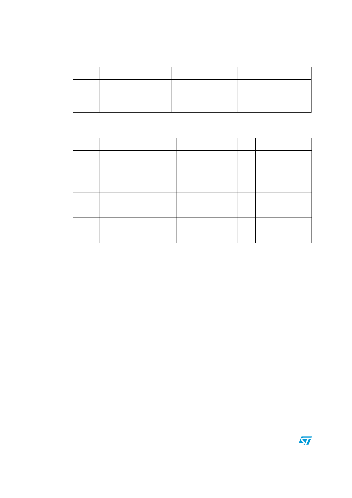
Table 7. Switching times
Symbol Parameter Test conditions Min. Typ. Max Unit
t
d(on)
t
d(off)
Turn-on delay time
t
Rise time
r
Turn-off-delay time
t
Fall time
f
Table 8. Source drain diode
= 50 V, ID = 4 A,
V
DD
RG = 4.7 Ω, VGS = 12 V
(1)
6
4
13
3
10.5
10.5
21.5
5.5
15
17
30
8
Symbol Parameter Test conditions Min. Typ. Max Unit
I
I
SDM
V
SD
t
rr
Q
I
RRM
t
rr
Q
I
RRM
1. Refer to the Figure 16: Source drain diode.
2. Pulse width limited by safe operating area.
3. Pulsed: pulse duration = 300 µs, duty cycle 1.5%
4. Not tested in production, guaranteed by process.
Source-drain current
SD
(2)
Source-drain current (pulsed)
(3)
Forward on voltage
(4)
Reverse recovery time
(4)
Reverse recovery charge
rr
(4)
Reverse recovery current
(4)
Reverse recovery time
(4)
Reverse recovery charge
rr
(4)
Reverse recovery current
= 8 A, VGS = 0
I
SD
= 8 A, VGS = 0,
I
SD
TC = 125 °C
= 8 A, di/dt = 100
I
SD
A/µs
= 17 V, Tj = 25 °C
V
DD
= 8 A,
I
SD
di/dt = 100 A/µs, VDD=
17 V, Tj = 150 °C
196 245
1.2
10
282 352
1.7
10.5
6
24
1.5
1.275
294 ns
422 ns
ns
ns
ns
ns
A
A
V
µC
A
µC
A
6/18 Doc ID 010029 Rev 2
Page 7
STRH8N10 Radiation characteristics
3 Radiation characteristics
The technology of the STMicroelectronics rad-hard Power MOSFETs is extremely resistant
to radiative environments. Every manufacturing lot is tested for total ionizing dose, according
to the ESCC 22900 specification window 1, using the TO-39 package. Both pre-irradiation
and post-irradiation performances are tested and specified using the same circuitry and test
conditions in order to provide a direct comparison.
(T
= 22 ± 3 °C unless otherwise specified).
amb
Total dose radiation (TID) testing
One bias conditions using the TO-39 package:
–V
The following parameters are measured (see Table 9, Table 10 and Table 11):
● before irradiation
● after irradiation
● after 24 hrs @ room temperature
● after 168 hrs @ 100 °C anneal
bias: + 15 V applied and VDS= 0 V during irradiation
GS
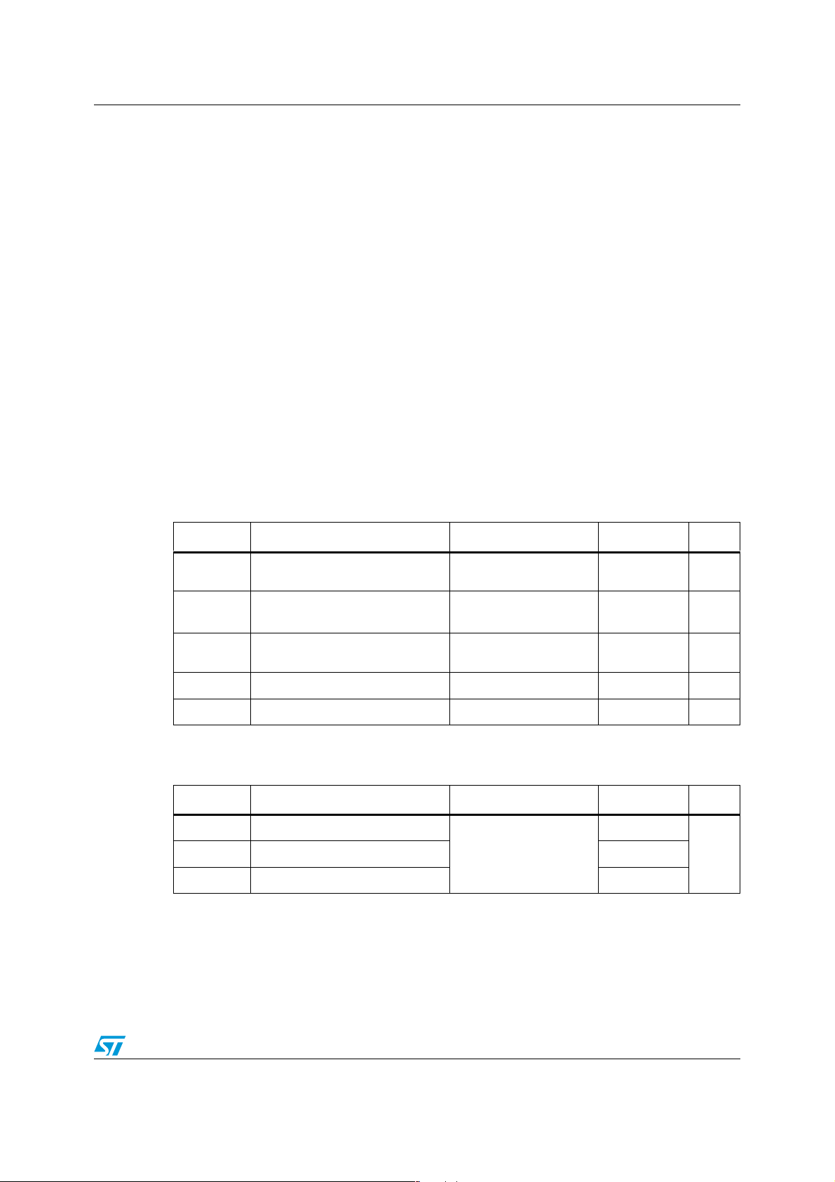
Table 9. Post-irradiation on/off states @ T
= 25 °C, (Co60 γ rays 70 K Rad(Si))
J
Symbol Parameter Test conditions Drift values ∆ Unit
I
I
BV
V
GS(th)
R
DS(on)
DSS
GSS
DSS
Zero gate voltage drain current
(VGS = 0)
Gate body leakage current
(VDS = 0)
Drain-to-source breakdown
voltage
80% BV
V
V
V
Dss
= 20 V
GS
= -20 V
GS
= 0, ID = 1 mA -25% V
GS
+1 µA
1.5
-1.5
Gate threshold voltage VDS = VGS, ID = 1 mA -60% / + 30% V
Static drain-source on resistance VGS = 10 V; ID = 4 A ±10% Ω
Table 10. Dynamic post-irradiation @ TJ= 25 °C, (Co60 γ rays 70 K Rad(Si))
Symbol Parameter Test conditions Drift values ∆ Unit
Q
Q
gs
Q
gd
Total gate charge
g
= 0.2 mA, VGS = 12 V,
I
Gate-source charge ±35%
G
VDS = 50 V, IDS = 4 A
Gate-drain charge -5% / + 130%
-5% / + 40%
nA
nC
Doc ID 010029 Rev 2 7/18
Page 8
Radiation characteristics STRH8N10
Table 11. Source drain diode post-irradiation @ T
Rad(Si))
Symbol Parameter Test conditions Drift values ∆.Unit
(2)
V
SD
1. Refer to Figure 16.
2. Pulsed: pulse duration = 300 µs, duty cycle 1.5%
Forward on voltage I
(1)
= 8 A, VGS = 0 ±2% V
SD
= 25 °C, (Co60 γ rays 70 K
J
Single event effect, SOA
The technology of the STMicroelectronics rad-hard Power MOSFETs is extremely resistant
to heavy ion environment for single event effect according to MIL-STD-750E method 1080
(bias circuit in Figure 3: Single event effect, bias circuit) SEB and SEGR tests have been
performed with a fluence of 3e+5 ions/cm².
The accept/reject criteria are:
● SEB test: drain voltage checked, trigger level is set to V
soon as a SEB occurs or if the fluence reaches 3e+5 ions/cm².
● SEGR test: the gate current is monitored every 100 ms. A gate stress is performed
before and after irradiation. Stop condition: as soon as the gate current reaches 100 nA
(during irradiation or during PIGS test) or if the fluence reaches 3e+5 ions/cm².
The results are:
– no SEB
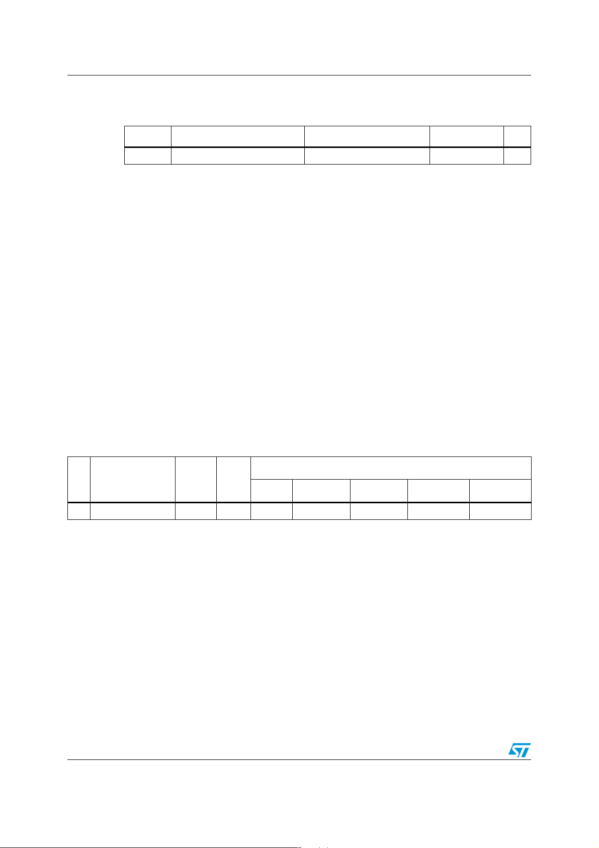
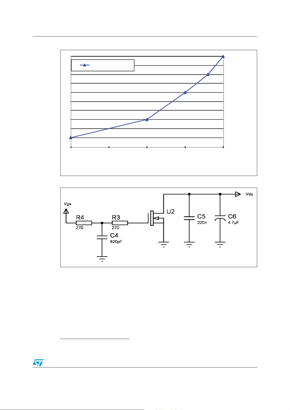
– SEGR test produces the following SOA (see Table 12: Single event effect (SEE),
safe operating area (SOA) and Figure 2: Single event effect, SOA)
= - 5 V. Stop condition: as
ds
Table 12. Single event effect (SEE), safe operating area (SOA)
V
(V)
Energy
Ion
Let (Mev/(mg/cm
Kr 32 768 94 100 80 60 30 10
2
)
(MeV)
Range
(µm)
@V
=0 @VGS= -2 V @VGS= -5 V @VGS= -10 V @VGS= -20 V
GS
DS
8/18 Doc ID 010029 Rev 2
Page 9
STRH8N10 Radiation characteristics
Figure 2. Single event effect, SOA
100
Kr (32 MeV .cm²/mg)
-20 -15 -10 -5 0
Vgs (V)
Figure 3. Single event effect, bias circuit
(a)
90
80
70
60
50
40
30
20
10
0
Vds (% Vdsmax)
a. Bias condition during radiation refer to Table 12: Single event effect (SEE), safe operating area (SOA) .
Doc ID 010029 Rev 2 9/18
Page 10
Electrical characteristics (curves) STRH8N10
25°C
-55°C
15 0 °C
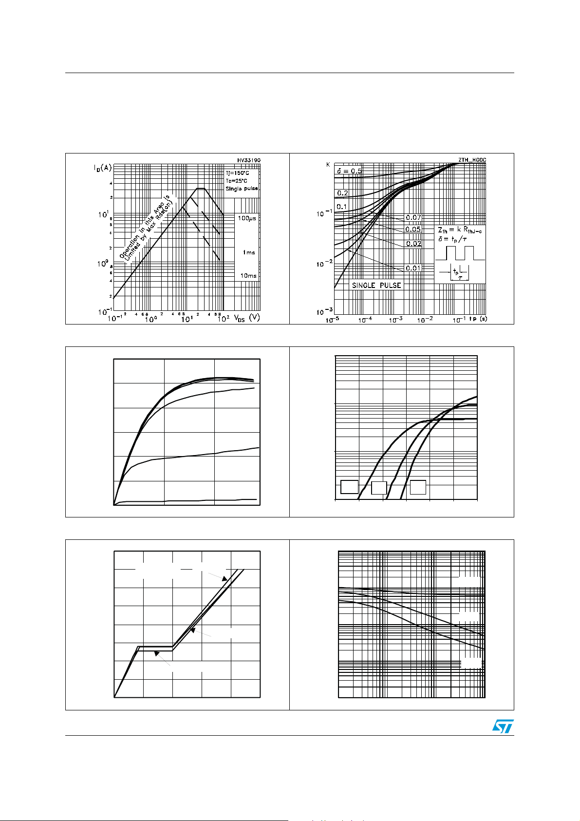
4 Electrical characteristics (curves)
Figure 4. Safe operating area Figure 5. Thermal impedance
Figure 6. Output characteristics Figure 7. Transfer characteristics
I
D
(A)
V
GS
= 10 V
25
HV33200
I
D
(A)
20
V
10.0
GS
= 7 V
15
V
GS
10
= 6 V
1.0
5
V
GS
= 5 V
0
0
Figure 8. Gate charge vs gate-source voltage Figure 9. Capacitance variations
V
GS
10
(V)
V
DS
= 50 V
I
D
20
= 8 A
V
DS
(V)
HV33210
12
0.1
3.50 4.00 4.50 5.00 5.50 6.00
C
(pF)
1000
10
8
D
= 4 A
I
100
6
4
I
D
= 2 A
10
2
0
0
10
5
15
20
Q
g
(nC)
1
0.1
1
10
VGS(V)
Ciss
Coss
Crss
V
HV33220
DS
(V)
10/18 Doc ID 010029 Rev 2
Page 11
STRH8N10 Electrical characteristics (curves)
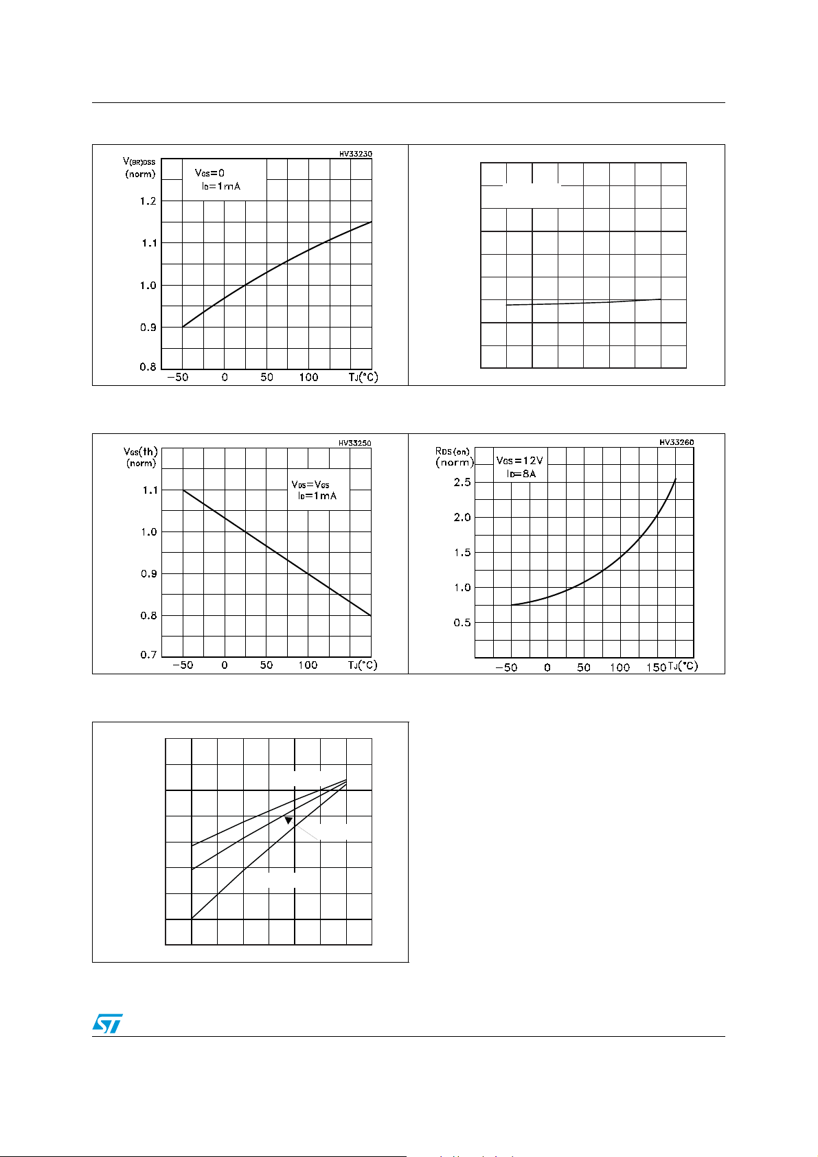
Figure 10. Normalized BV
vs temperature Figure 11. Static drain-source on resistance
DSS
Figure 12. Normalized gate threshold voltage
vs temperature
R
DS(on)
(mΩ)
800
VGS=12 V
700
600
500
400
300
200
100
0
1 3
24
567
I
Figure 13. Normalized on resistance vs
temperature
D
(A)
HV33240
Figure 14. Source drain-diode forward
characteristics
V
SD
(V)
1.3
1.2
1.1
1.0
0.9
0.8
0.7
0.6
1
2
j =
-50 °C
T
T
j =
25 °C
T
j =
150 °C
4
3
6
5
7
HV33270
I
SD
(A)
Doc ID 010029 Rev 2 11/18
Page 12
Test circuit STRH8N10
5 Test circuit
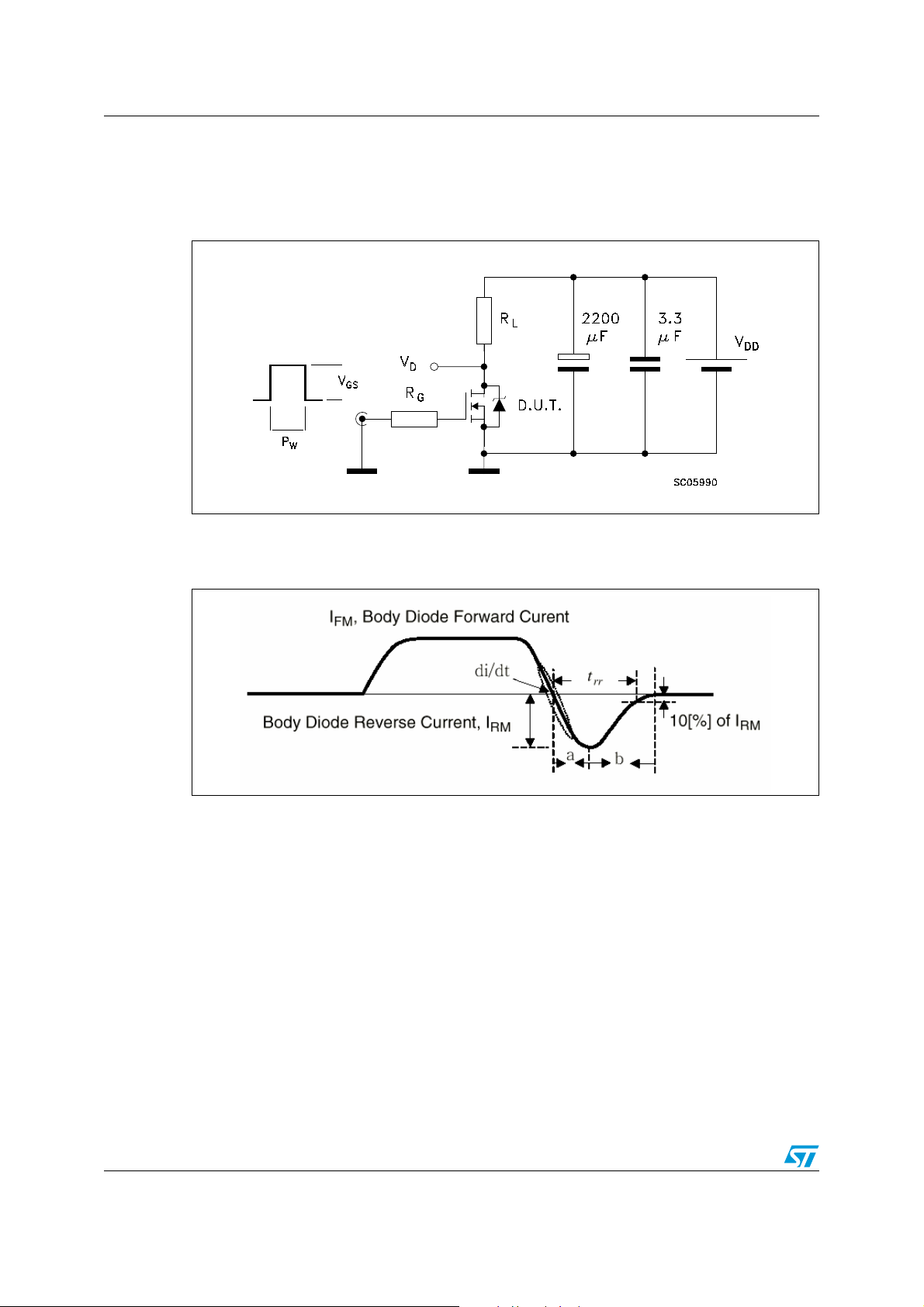
Figure 15. Switching times test circuit for resistive load
1. Max driver V
Figure 16. Source drain diode
slope = 1V/ns (no DUT)
GS
(1)
12/18 Doc ID 010029 Rev 2
Page 13
STRH8N10 Test circuit
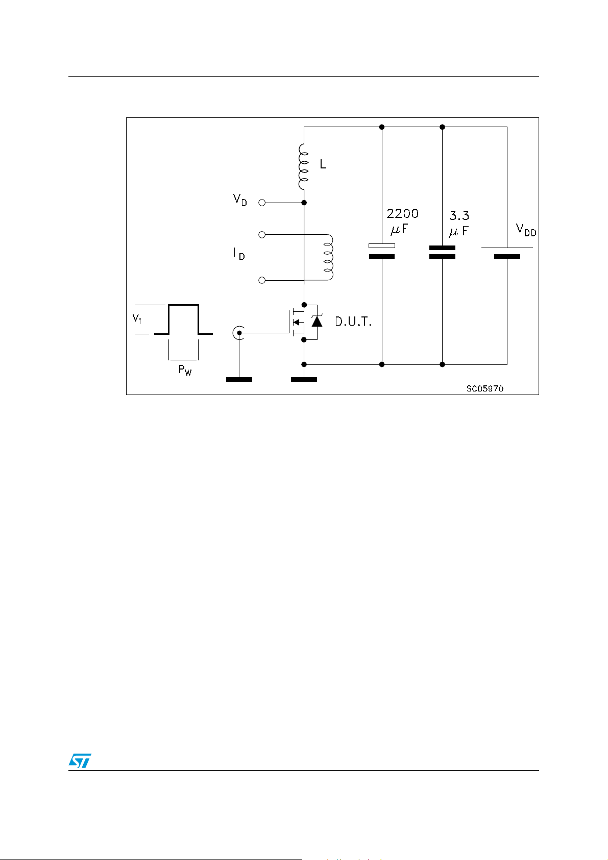
Figure 17. Unclamped inductive load test circuit (single pulse and repetitive)
Doc ID 010029 Rev 2 13/18
Page 14

Package mechanical data STRH8N10
6 Package mechanical data
In order to meet environmental requirements, ST offers these devices in different grades of
ECOPACK
specifications, grade definitions and product status are available at: www.st.com. ECOPACK
is an ST trademark.
®
packages, depending on their level of environmental compliance. ECOPACK®
14/18 Doc ID 010029 Rev 2
Page 15
STRH8N10 Package mechanical data
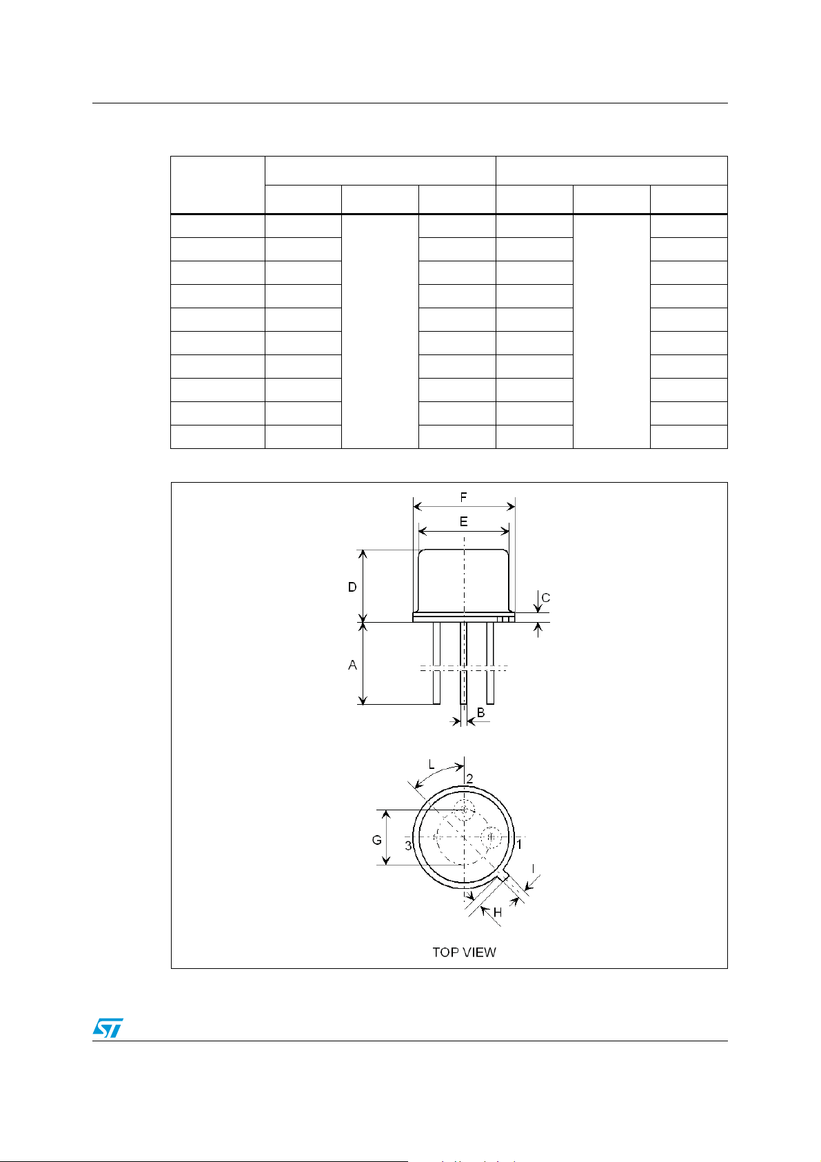
Table 13. TO-39 mechanical data
mm Inch
Dim.
Min. Typ. Max. Min. Typ. Max.
A 12.70
B 0.40 0.49 0.016 0.019
C 0.58 0.74 0.023 0.029
D 6.00 6.40 0.237 0.252
E 8.15 8.25 0.358 0.362
F 9.10 9.20 0.358 0.362
G 4.93 5.23 0.194 0.206
H 0.85 0.95 0.033 0.037
I 0.75 0.85 0.029 0.033
L 42° 48°
Figure 18. TO-39 drawing
14.20 0.500
-
-
0.559
Doc ID 010029 Rev 2 15/18
Page 16

Order codes STRH8N10
7 Order codes
Table 14. Ordering information
Order code
STRH8N10N1 -
STRH8N10NG TBD ESCC flight Target TBD
ESCC part
number
Quality
level
Engineering
model
EPPL Package
TO-39 Gold
Lead
finish
Marking Packing
STRH8N10N1
Strip
pack
Contact ST sales office for information about the specific conditions for products in die form
and other package options.
16/18 Doc ID 010029 Rev 2
Page 17

STRH8N10 Revision history
8 Revision history
Table 15. Document revision history
Date Revision Changes
20-May-2011 1 First release.
09-Nov-2011 2
Updated dynamic values on Table 6: Dynamic, Table 7: Switching
times.
Doc ID 010029 Rev 2 17/18
Page 18

STRH8N10
Please Read Carefully:
Information in this document is provided solely in connection with ST products. STMicroelectronics NV and its subsidiaries (“ST”) reserve the
right to make changes, corrections, modifications or improvements, to this document, and the products and services described herein at any
time, without notice.
All ST products are sold pursuant to ST’s terms and conditions of sale.
Purchasers are solely responsible for the choice, selection and use of the ST products and services described herein, and ST assumes no
liability whatsoever relating to the choice, selection or use of the ST products and services described herein.
No license, express or implied, by estoppel or otherwise, to any intellectual property rights is granted under this document. If any part of this
document refers to any third party products or services it shall not be deemed a license grant by ST for the use of such third party products
or services, or any intellectual property contained therein or considered as a warranty covering the use in any manner whatsoever of such
third party products or services or any intellectual property contained therein.
UNLESS OTHERWISE SET FORTH IN ST’S TERMS AND CONDITIONS OF SALE ST DISCLAIMS ANY EXPRESS OR IMPLIED
WARRANTY WITH RESPECT TO THE USE AND/OR SALE OF ST PRODUCTS INCLUDING WITHOUT LIMITATION IMPLIED
WARRANTIES OF MERCHANTABILITY, FITNESS FOR A PARTICULAR PURPOSE (AND THEIR EQUIVALENTS UNDER THE LAWS
OF ANY JURISDICTION), OR INFRINGEMENT OF ANY PATENT, COPYRIGHT OR OTHER INTELLECTUAL PROPERTY RIGHT.
UNLESS EXPRESSLY APPROVED IN WRITING BY TWO AUTHORIZED ST REPRESENTATIVES, ST PRODUCTS ARE NOT
RECOMMENDED, AUTHORIZED OR WARRANTED FOR USE IN MILITARY, AIR CRAFT, SPACE, LIFE SAVING, OR LIFE SUSTAINING
APPLICATIONS, NOR IN PRODUCTS OR SYSTEMS WHERE FAILURE OR MALFUNCTION MAY RESULT IN PERSONAL INJURY,
DEATH, OR SEVERE PROPERTY OR ENVIRONMENTAL DAMAGE. ST PRODUCTS WHICH ARE NOT SPECIFIED AS "AUTOMOTIVE
GRADE" MAY ONLY BE USED IN AUTOMOTIVE APPLICATIONS AT USER’S OWN RISK.
Resale of ST products with provisions different from the statements and/or technical features set forth in this document shall immediately void
any warranty granted by ST for the ST product or service described herein and shall not create or extend in any manner whatsoever, any
liability of ST.
ST and the ST logo are trademarks or registered trademarks of ST in various countries.
Information in this document supersedes and replaces all information previously supplied.
The ST logo is a registered trademark of STMicroelectronics. All other names are the property of their respective owners.
© 2011 STMicroelectronics - All rights reserved
STMicroelectronics group of companies
Australia - Belgium - Brazil - Canada - China - Czech Republic - Finland - France - Germany - Hong Kong - India - Israel - Italy - Japan -
Malaysia - Malta - Morocco - Philippines - Singapore - Spain - Sweden - Switzerland - United Kingdom - United States of America
www.st.com
18/18 Doc ID 010029 Rev 2
 Loading...